Note: Descriptions are shown in the official language in which they were submitted.
WO 91/19220 PCr/VS91/02û13
~$~
OPTICAL PAR~METRIC AMPLIFIER
CROSS-REFERENCE TO RELATED PATENT APPLICATION
The subject matter of this patent application
is related to that disclosed in patent application
S.N. ~0S,501, filed Septem~er 11, 1989.
BACKGROUND OF THE INVENTION
An optical paramet~ic amplifier typically
comprises a material that has a nonlinear, i.e.,
amplitude-dependent, response to each incident
light wave. In addition ~o an informaticn-
modulated wave to be amplified, a pumping wave of
another f~equency is applied to the material to
interact with and transfer energy to the
:15 information-modulated wave.- The~amplification of
the information-modulated wave produced by this
transfer of energy~is called parametric gain.
~`:The main line of development:both of optical
second harmonic generators and of optical
parametric ~mplifiers has centered around the use
~ - of birefringent~ materials ~o o~tain phase
; :m~tching, which enables traveling wave parametric
,
'~
.
WO91/192~0 P~T~US91/~2nl3
amplification. Phase matching is the process of
making the sum of the signal and idler wave
vectors equal to the pumping wave vector. A wa~e
vector is related to the product of index of
refraction and frequency, or to index divided by
wavelength.
In general, classical phase matching (e.g.,
Yia angle or thermal tuning) requires a certain
combination of intrinsic birefringence and
dispersion of refractive indices. New small
molecular weight crystalline organic nonlinear
optical materials with high second harmonic
susceptibility have been reported in literature
such as ACS Symposium, Series No. 233, pages 1-26,
1983 by Garito et al. These organic materials
usually possess high intrinsic birefingenc~ and
positive dispersion so that phase ma~ching can be
achieved with a sin~le crystal. Even if phase
matching can be achieved with ~he new types of
organic materials`having high nonlinear optical
susceptibility/ the low beam power of a diode
laser significantly limi~s the power conversion
efficiency~ The high birefringence of the organic
matarials also l~wers the conversion efficiency
because of beam walk-off.
An alternative means to arhieve phase matched
conditions is the use of dispersion properties for
different modes in a waveguide. Since the energy
i~ confined laterally to a narrowly constricted
space, a high light intensity is possible with a
WO91/19220 PCTtUS91/02013
;~ 4~1.
relatively low power source. If the waveguide
geometry and refractive indices of the guiding
region and cladding region are such that:
., .
J3 = ~3n ( (~3 ) ~ Bm ~ ~')2 ~ ) = ( 1 )
;
then the phase matching condition is established.
Here, B; is the propagation constant of the i-th
mode. The con~ersion efficiency is generally
~( quadratically dependent on the overlap integral
.l~ between the modes:
.~ .
~ lO F fEn(~3~ z)Em(~2, z)E~ , z)dz
: .
where Ek is the normalized elec~ric field of the
k-th mode a~ross the waveguide. In general, the
overlap between the waveguide modes is limited,
a~d the value~of the overlap intQgral is also
lS ~small. This approach has been utilized f~r second
harmonic generation phase matching in waveguides
dex~ived~rom~organic materials, as reported in
Optics Commun~ 47, 347 (1983) by
. Hewi~ et al. However, the le~el of second
ZO harmonic conversion efficiency is low, suggesting
no-practical param tric amplificativn application.
Of background interest with respect to the
present invention are United States Patent Numbers
3,267,385; 3,660,673; and 3,831,038 which describe
: ~
WO91/19220 PCT/US91/02013
optical parametric amplifier devices with
inoryanic nonlinear optical waveguiding means.
Also of interest is literature relating to
spatially periodic nonlinear structures for
modulation of electromagnetic energy. The
pertinent literature includes IEEE J. of Quantum
Elect., QE-9 (No. 1), 9 (1973) by Tang et al;
Appl. Phys. Lett., 26, 375 (1975) by Levine et al;
Appl. Phys. ~ett., 37(7), 607 (1980) by
Feng et al; and United States Patent Numbers
3,384,433; 3,407t309; 3,688,124; 3,842,289;
3,93S,472; and 4,054,362.
The thin film waveguides with a periodically
modulated nonlinear optical coefficient as
described in the literature are either inorganic
op~ical substrates with material fabrication
disadvantages,` or they are organic materials which
are in the liquid phase, such as a liq~id crystal
medium or a thin film of nitrobenzene which
reguire a continuously applied external DC
ele~tric fiéld.
of particular interest with respect to the
present inYention is literature relating to the
dispersive properties of a thin film optical
waveguide for TE and TM modes, as expressed in
analy ic terms defining the variation of the
effective re~ractive index with respect to one or
more physical parameters in the waveguiding
medium. The per~inent li~erature includes
J. Appl. Phys., 49(9), 4945 (1978) by Uesugi et
al; Appl. Phys. Lett., 36(3), 178 (1980) by
Uesugi; Nonlinear Optics: Proceedings Of The
:
WO91/19220 PCT/US91/02013
41.
International School Of Materials Science And
Technology, Erice, Sicily, July 1-14, 1985
~Springer-Verlag), pages 31-65 by Stegeman et al;
Integrated Optics, Volume 48, pages 146-151 by
Ostrowsky (Springer-Verlag, 198S); Integrated
Optics, Volume 48, pages 196-~0~ by Bava et al
(Springer-Verl~g, 1985); and Appl. Opt., 25(12),
1977 (1986) by Hewak et al.
There is continuing interest in the
devel~pment of compact and efficient nonlinear
optical devices, such as parametric oscillators
and amplifiers.
Accordingly, it is an object of this
invention to provide an optical parametric
amplifier device with an organic nonlinear optical
waveguiding medium which is adapted to amplify the
intensity of an input signal béam.
It is another object of this invention to
provide an optical parametric amplifier device
w~th a polymeric nonlinear optical waveguide
~: chann l having~a spa~ial periodic structure for
quasi-phase matching of propagating wave vectors,
and with a:refrac~ive index tuning means for
ef~icient phase matching~
: 25 ~ Othèr~objects and advantages of the present
invention shall become apparent from the
accompanying description and drawings~
!
~ '
:: :
WO 91/19221) PCI/US91/020t~
DESCRIPTION OF THE INVENTION
One or more objects of the present invention
are accomplished by the provision of an integrated
optical parametric amplifier which comprises ~1) a
light signal source and t2) a laser beam source,
in coupled combination with (3) an optical
waveguide with a waveguiding matrix consisting of
an organic film medium which exhibits second order
nonlinear optical response, and which has a
spatial periodic structure for quasi-phase
matching of propagating waves; wherein the
coherence length Qc ~ the waveguide periodic
organic medium is defined by the equation:
7r
Q
::
where ~B is the propagation constant difference
which~is equal~to B(~p)~ s)-B(~ p is the pump
~r~quency,~ 9 iS: the~signal fre~uency,and ~j is
~ ~ ~ the i~ler frequency.: : ~ ~
;; In another embodiment this in~ention provides
an integrated optical parametric ampli~ier which
c~mprises~ a~1ight signal source with a
wavelength:;of about 0.5-2 ~m, and (2~ a laser beam
source with~a~:wavelength of about 0.6-1~3 ~m, in
coupled combination with (3) an optical waveguide ! '
comprising a two-dimensional channel structure for
single mode:wave transmission, and the channel
:~:
WO91/19220 PCT/~'S91/02013
Z~3~
waveguiding matrix comprises a polymer medium
which exhibits second order nonlinear optical
response, and which has a spatial periodic
structure for quasi-phase matching of propagating
waves; wherein the coherence length ~c of the
periodic pol~mer medium is in the range of about
lO-lO0 ~m, and is defined by the e~uation:
c Q~
where ~ is the propagation constant difference
which is equal to B~p)-B(~s)~ p is the pu~p
frequency, ~5 is the signal frequency,and ~j is
the idler frequency; and wherein the output wave
energy under operating conditions comprises the
incident laser beam, a generat d idler beam, and
an amplified signal beam.
In a further embodiment this invention
: provides an integra~ed optical parameter amplifier
which comprises (l) a light signal source with a
wavelength of about 0.5-4 ~m, and~2~ a laser beam
source with a wavelength of about 0.6-l.3 ~m and a
power level of about 50-lO00 mw, in coupled
: combination with (3) an optical waveguide
comprising a two-dimensional channel structure for
single mode~wave transmission,'and the channel
2~ waveguiding matrix comprises a side chain polymer
medium which has an external field-induced
noncentrosymmetric molecular orientation of side
chains and a nonlinear optical coefficient d of at
:
~ WO91/19220 PCT/US91/02013
;~t~
least about lO pm/V, and which has a spatial
periodic structure for quasi-phase matching of
propagating waves; wherein the coherence l~ngth ~c
. of the waveguide periodic polymer me~ium is in the
i 5 range of about l.0-.lO0 ~m, and is defined by the
.~ equation:
i . . , ~ .
Q. = _
c ~
where ~ is the propagation constant difference
which is equal to B~p)-B(~s)~ p is the pump
frequency, ~s is the signal fre~uency, and ~; is
i the idler frequency; and wherein the output wave
energy under operating conditions comprises the
incident Iaser beam, a generated idler beam, and
an amplified signal beam with a gain G of abo~t
10-1000. ~ ~
An ~ptical parametric amplifier inherently is
a narrow band device, e.g., a~out 3 nmO The
bandwidth range of the device can be broadened by
utilizati~n~of:;a~chirped type of periodic
: configuration in the waveguiding medium. In a
: chirped periodic configuration, the coherence
length ~aries across the grating structure.
A parametric amplifier as defined hereinabove
can be in further combination with electrodes for
the application of an electric field to the
organic waveguiding medium, and additionally with
filter means to absorb the incident laser beam and
'
~ :
WO91/19220 PCT/US91/02013
;~v~
generated idler beam from the output wave energy
spectrum. Another means of isolating the output
amplified signal beam is to employ a detector
which senses only the signal beam.
Another preferred variation in optical
parametric amplifier design is the inclusion of a
heat control means for temperature tuning and
phase matching of the propagating wave energy
under operating conditions.
An invention optical parametric amplifier can
be fabricated with a two-dimensional waveguide
having channel dimensions w of 5 ~m, a refractive
index n of l.6, and a nonlinear optical
coefficient d of lO0 pm/Y. When Pp is O.l W,
As i5 1. 3 ~m and ~p is 0.8 ~m under operating
conditions, with an assumed absorption coefficient
of 4/cm, an exponential gain coefficient g of
6.4/cm, and a gain G of lO00 is obtained.
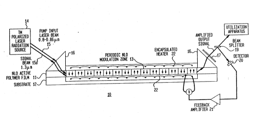
Referring to the drawings, FIG. l is a
perspective Yiew of an integrated optical
parametric~ampli~ier i~ accordance with the
present invention.
FIG. 2 is~a representation of side view
sect-Ions of~a;FIG. l~type waYeguide thin film,
illustrating alternating poled molecularly
oriented domains in one section, and poled
molecularly oriented domains alternating with
unpoled domains in the other section.
~ FIG~ 3 is a schematic drawing of a FIG. l
type of optical parametric amplifier with a two-
dimensional channel waveguide design.
WO91/l9220 PCT/VS91/02V13
Thin film waveguide 10 in FIG. 1 is a
composite construction of substrate 12 which
supports nonlinear optically active polymer film
11. A linear ~ection of polymer film 11 consists
of periodic nonlinear optical modulation zone 13.
In practice thin film waveguide 10 is
utilized in combination with transverse magnetic
(TM) polarized laser radiation source 14 which
provides input pump laser beam 15 and input signal
beam 15a; a pair of prism coupling means 1~ which
couple laser beam 15 and signal beam 15a to
polymer film 11; filter 17, and utilization
apparatus 18, such as a communications system.
Beam splitter 19 is utilized to direct a
portion of the output signal to detector 20, which
drives feedback amplifier 21. The heater 22 units
are temperature controlled within a + 0.5C range,
and the temperature is maintaihed at the point of
maximum phase matched X~2? generation as monitored
- 20 by the signal detection means.
The input TM polarized coherent
electromagnetic radiation preferably is a laser
beam such-as that genera~ed by a diode laser with
a wayelength in the 0.8-0.~6 ~m range.
: 25 The coupling means can consist of a pair of
prism couplers, such as Scho~t SF6 optical glass
with a high index of refraction. Optical coupling
and decoupling also can be accomplished with
optical diffraction gratings which are formed
directly on the surface of the thin film
.
WO91/19220 PCT/US91/02013
~ *1.
11
waveguide, as described in United States Patents
3,674,335; 3,874,782; and 3~90,775. Another
coupling means is through the cleaved end faces of
a waveguiding structure, as shown in FIG. 3.
The substrate 12 as illustrated in FIG. l can
be constructed of any convenient non-conducti~g
~, medium such as pl~stic, glass, or silicon oxide.
The heater units 22 typically are
~sncapsulated in a ceramic or other inorganic
medium, or in a polymer medium such as an epoxy
resin.
The organic thin film waveguiding medium of
an invention optical parametric amplifier device
is transparent, either liquid crystalline or
amorphous in physicaI properties, and exhi~its
second order nonlinear optical response. The
organic medium has a higher refractive index
(e.g., 1.5~ than the supporting substrate, or
higher than the cladding layer (e.g., sputtered
silica or an organic material) if one is
compos1ted between the polymer medium and the
suppor~ing su~strate.
The transparent polymer medium can be applied
to the supporting substrate by conventional
~5 methods, such as spin coating, spraying,
Langumir-Blodgett deposition, and the like.
T~e term "transparent" as employed herein
refers to an orga.nic,thin film waveyuide medium
which is transparent or light transmitting with
: 30 respect to inciden~ fundamental and created light
WO91/1g220 PCT/US91/0201~
~3~ 12
frequencies. In a present invention waveguide
parametric amplifier device, the organic thin film
nonlinear optical waveguiding medium is
transparent to both the incident and exit light
frequencies.
The term "amorphous" as employed herein
refers to a transparent polymeric optical medium
which does not have a preferred short range
molecular order that exhibits optical anisotropy.
The term "external field" as employed herein
refers to an electric, magnetic or mechanical
stress field which is applied to a substrat of
mobile organic molecules, to induce dipolar
alignment of the organic molecules parallel to the
field.
The term "parametric" as employed herein
refers to interactions in wave energy states in an
optical medium in which time variations in an
input signal are translated into different time
variations in an output signal as determined by an
operative nonlinearity parameter.
A present invention organic thin film
waveguide medium preferably is a polymer having a
comb struçture~o~ side chains which xhibit
nonlinear optical;response. This type of chemical
~structure is:illustrat:ed:by thermopla~tic polymers
which are haracterized by a recurring mono~eric
unit corresponding to the formula:
: , .
:
:;
WO91/19220 PCT/US91/02013
.
13
. [ I '~
I '
M'
where P' is a polymer main chain unit, S' is a
flexible spacer group having a linear chain length
of between about 2-20 atoms, M' is a pendant group
which exhibits second order nonlinear optical
susceptibility, and where the pendant groups
comprise at least about 25 weight percent of the
polymer, and the po~ymer has a glass transition
temperature or~softening poin~ above about 40C.
~ mong the~preferred:types of side~chain
polymers ~re;those characterized by a recurring
monomeric unit corresponding to the formula:
:
15 : ~ R
O~ 2) n-x~=~cH=cH~ -z or
. R i ,
~ : 20 ~C~2-f~
~(CH~)n~X~;3
~ ~.
: ~ ~
WO91/19220 PCT/VS91/02013
$, ~
14
where m is an integer of at least 5; n is an
integer between about 4-20; X is -NR-, -O- or -S-;
R is hydrogen or a C1-C4 alkyl; and Z is -NOz, -CN,
-CF3, -CH=C(CN)z, -C(CN)=C(CN)z or -SO2CF3.
Side chain polymers of interest are described
in U.S. 4,694,066~ Illustrative of side chain
~olyme~ species are poly~6-(4-nitrobiphenyloxy)-
hexyl methacrylate,}, poly(L-N-p-nitrophenyl-2-
piperidinemethyl acrylate), and stilbene-
containing polymers such as:
-~-O-CH2-~H~
( CH2 ) 2-NH~CH=(: H~ N~2
A preferred type of side chain polymer is the
copolymer structure~discloced in~U.S. 4,865,430.
An essenti:al feature of a present invention
: optical parametric amplifier device is a periodic
nonlinear optical modulation zone~13 as
~ represented in Fiq~.~l. The periodicity of a
: waveguide ~LO~modulation zone preferably is
` 20 accomplished~by poling with an electric field to
~achieve orientation of the organi~c molecules
parallel to the direction of the electric field.
The poling induces a microscopic noncentrosymmetry
in the poled domains of the organic medium, and
:~ . 25 establishes:second order nonlinear optical
susceptibility in the organic medium.
- ,
WO91/19220 PCT/US91/02013
Poling of a thin film waveguide medium can be
accomplished conveniently by heating the medium
near or above its melting point or glass
transition temperature, then applying a DC
electric field (e.g., 50-150 V/~m) to the medium
to align molecular dipoles i~ a uniaxial
orientation. The medium then is cooled while the
medium is still under the influence of the applied
DC electric field. In this manner a stable and
permanen~ molecular orientation is immobilized in
a rigid structure within the poled domains.
The poling can be applied to an organic
medium that is substrate-supported, by an
appropriate placement of upper and lower electrode
units, where one of which has a grating
configuration.
In another invention embodiment, cladding
layers are employed which are in the form of
organic films~exhibiting second order nonlinear
optical response and having a lower index of
xefraction~than the waveguiding organic medium.
In a typical waveguide ~onstruction, the organic
waveguiding medium and cIadding layers are side
chain,polymers,~ respectively, all of which can be
: ~ 25 molecul~rly oriented~simultaneously during an
electric fi ld poling cycle.
The followin~ examples are further
illustrative of the present invention. The device
components are presented as being typical, and
30 various modifications in design and operation can
~ ~b derived in:view of the foregoing disclosure
: ~ wiehin the scope of the invention.
:
:
W091/19220 PCT/US91/02013
~`3~
; 16
EXAMPLE I
This example illustrates the construction and
operation of an optical parametric amplifier in
accordance with the present invention.
The material refractive indices are measured
at 0.8626 ~m, 1.34 ~m and 2.42 ~m corresponding to
the pump, signal and idler wavelengths used in the
device fabrication. For a (50/50) methyl
methacrylate/4-[N-(2 methacroyloxyethyl~-N-
methylamino]-4'-nitrostilbene waveguiding medium
the indices are 1.6514, 1.6258, and 1.6161,
respectively. For the cladding material
(Norland 60 epoxy~ the indices are 1.549, 1.545
and 1.543, respectlvely.
The periodicity of the waveguide is a
function of the~polymer medium dispersion, and
also of the waveguide dispersion. Maxwell's
equations for a thin film waveguide are solved for
TM modes:~or the pump, signal and idler beams,
respectively. The calcula~ed periodicity i~
20.2 ~m~ ~
A periodic poled wavegulde is fabricated in
accordance with the following procedure. A
commercially~ava~ilable silicon dioxide coated
silicon wafer is placed in a Varian electron beam
vacuum deposition~system. A 200 ~ layer of
99.999% purity aluminum is deposited on the wafer.
Az-1518 positiv~ photoresist (Hoechst) is
spin coated on the aluminum coated wafer with a
Soltec model 5100 coater. A 1.5 ~m photoresist
WO9t/19220 PCT/US91/~2~13
3~
coating is achieved by spinning at 5000 rpm for
30 seconds. The pho~oresist coatiny is dried in a
vacuum oven at 90C for 30 minutes.
The photoresist coating is patterned by
placing the wafer in contact with a mask of the
desired periodicity in a Karl Suss model MJB 3
mask aligner, and exposing the masked coating to
405 nm radiation (70 mJ/cm2).
The patterned photoresist is developed with
AZ developer in water (1:1) over a period of
60 seconds, and the developing cycle is terminated
by washing with deionized water.
The photoresist coating of the wafer is baked
in a vacuum oven at 120C for 45 minutes. The
exposed aluminum pattern is etched with type A
etchant (Transene Corp.) at 50C for 20 seconds,
and the etched surface is rinsed with deionized
~ater. The periodicity of the electrodes is
20 ~m.
: 20 The aluminum grating electrode surface of the
wafer is covered with 1.8 ~m cladding layer
(Norland:60 epoxy) by spin coating at ~500 rpm for
30 seconds at 35 C, and the cladding layer is
cured,by ultra~iolet radiation at 15 mW/cm2 for
: 25 4 minutes.
A nonlinear optically ac~ive organic laye~ of
2 ~m thickness of the above-identified 50/50
polymer is ~pin coated on the cladding layer at
~500 rpm. The spin coating medium is a 20%
solution of the polymer in cyclohexanone. The
WO9~/19220 PCT/US91/0201
,~ , 18
polymer layer is dried in a vacuum oven at 160C
for 2 hours, and then cooled down slowly.
An upper cladding layer of l.8 ~m thickness
is added by spin coating a medium of Norland 60
epoxy resin at 9500 rpm for 30 seconds at 35C.
The cladding layer is cured by ultraviolet
radiation at 15 mW/cm2 for 4 minutes. A lOO0 A
coating of gold is deposited as an electrode layer
on the upper cladding layer.
The waveguide structure is cleaved at
opposite ends to provide two sharp faces to couple
light in and out of the polymer waveguiding
medium. Wires are attached to the top and bottom
electrodes~ The waveguide is poled by placing it
in a Mettler~hot stage. It is heated at 1C/min
to Tg at 9OC, and a field of 70 V/~ is applied
for 5 minutes. Then the waveguide is cooled at
; 0.2~C/min~to room~temperature while maintaining
the electric~field.~;The poled waveguiding medium
20 ~has~a nonlinear~optical~coefficient d of about
80 p~/V. ~
~An~optica~l arrangement for~testing the
~parametric~amplifier is as follows. A Quantel TDL
50 d~e laser~is employed to pump a H2 Raman cell
~ 25 to produce~O~.862~6 ~m and 1.34 ~m light as the
; ~irst~ and second~Stokes lines, respectively. The
:
first Stokes line is intense and acts as the pump
for the parametric àmplifier, and the weaker
second Stokes line functions as the signal beam
which is going to be amplified. ~The ~wo beams are
'
~::: ::
WO91t19220 PCT/US91/02U13
19 ;~
emitted from the H2 cell colinearly, and are
directed by a focussing lens into the waveguiding
medium. Interference filters allow adjustment of
the pump power into the waveguide, while leaving
the signal intensity unchanged. Interference
filters are placed after the waveguide to block
the pump at 0~8626 ~m. The idler produced at
~.42 ~m also is not detected because the detectors
utilized did not respond at that wavelength.
Two methods are employed to detect the
amplified signal at l.3 ~m. The first method is
the use of a germanium detector. ThP second
method is based on the fact that the l.3 ~m signal
produces a second harmonic at 0.65 ~m, since the
lS waveguide is also a second order nonlinear optical
x2) medium. By placing a narrow pass filter at
0.65 ~m on a photomultiplier tube, a suitable
signal to noise discrimination against background
is obtained.
The waveguide is placed on a hot stage with a
+ 0.5C temperature control. The hot s~age is
mounted on a rotation stage such that the
effective periodicity of the grating can be
changed by angling of the incident beams. l.3 ~m
light is coupled into the waveguide and detected.
At the~correct periodicity where phase matching
occurs, the pump at 0.86 ~m also is coupled into
the waveguide, resulting in an amplified l.3 ~m
signal. The polarization of the input and output
signals is TM, indlcating that the d33 coefficient
: ~ .
WOgl/19220 PCT/US91/02013
~3~ ~.
had been phase matched. Away from the phase
matching periodicity, no amplification is
ohserved.
Additional methods of tuning are by changing
the temperature of the waveguide which results in
large changes in refractive indices, and by
~pplying a voltage across the waveguide which
results in small changes in refractive indices.
In another embodiment side chain polymer
cladding layers are utilized which exhibit second
order nonlinear optical susceptibility, and which
have a lower index of refraction than the
waveguiding medium.
WO9l/19220 PCT/US91tO2013
21
EXAMPLE II
This Example illustrates the construction and
operation of a two-dimensional rib waveguide for
optical parametric amplification in accordance
with the present inve~tion.
Following the procedures of Example I, an
oxidized silicon substrate (2 microns of SiO2 on
Si) is coated with an aluminum graking electrode.
A thin ~1000 angstroms) polysiloxane layer is
spin~coated from a 7% solution at 4000 rpm and
cured for 45 minutes at 110C. A spin-coated
Master Bond W 11-4Ml epoxy (Master Bond Inc.)
layer 2 microns thick is deposited by spin-coating
at 3000 rpm, and curing for 20 minutes under a
i5 25 mw/cm2 u.v. mercury-xenon arc lamp. The
surface is treated by exposure to a 5 watt r.fO
oxygen plasma in a reactive-ion-etcher for
5 seconds and is coated with a nonlinear opti~ally
active organic layer (1.25 microns) as in
Example I. A secvnd;epoxy layer is applied as
described above and~cured for 5 minutes.
; ~he upper cladding layer is coated with an
aluminum ma~king layer (2000 angstroms). A narrow
AZ-1518 photoresist ribbon-like strip (5.5 microns
2S in width) is caated on the aluminum in the
waveguidin~ direc~ion of the laminated structure.
The aluminum not covered by the photoresist is
removed as in Example I. The upper surface of the
wav~guide s~ructure is exposed to reactive ion
etching to romove the multilayers down to the
WO91/19220 PCT/~'S91/02013
22
bottom polysiloxane layer, except for the
photoresist coated strip. The etching cycles also
remove the photoresist coating from the aluminum
strip. The aluminum coating is removed from the
ribbon-like strip o~ multilayers. The substrate
and the upper surface multilayer strip are spin-
coated with Master Bond W l1-4Ml epoxy at
2500 rpm, and the coating is cured by means of the
above described conditions.
Following the procedures of Example I, an
upper aluminum grating electrode (lO00 angstroms)
is constructed on the upper epoxy layer, and the
nonlinear optically active polymer layer is
molecularly oriented by means of a DC field
applied between the electrodes. The poled
waveguiding medium has a nonlinear optical
coefficient d of about lO0 pm/V.
The two endfaces in the waveguiding direction
are cleaved for end-fire coupling of light into
and out of the two-dimensional wa~eguiding
~hannel.
The fine adjustment of the waveguide X(
.~
period to match the polymer channel~ coherence
length is accomplished by electroop~ic kuning of
the linear refractive index by application of an
electric field between the electrodes, or by
temperature adjustment.
The waveguide is coupled with a Quantel TDL
509 dye laser and H2 Raman cell, and a signal beam
is amplified in the manner described in Example I.
: ~:
.