Note: Descriptions are shown in the official language in which they were submitted.
The invention relates to a remote-controlled
master switch facility of a telecommunications network.
In the course of the privatization of
telecommunication connections, from a certain point
onwards, the so-called interchange point, subscribers can
freely install and use their own private telephone or
telephone system. The maintenance of such private
telephone systems lies in the hands of the private
operator, and is not the responsibility of the network
provider. In the case of a disturbance or fault, it is
thus particularly useful to the network provider to be able
to as easily as possible determine whether the fault has
occurred within his network or within the private telephone
system, since the network provider is only responsible for
eliminating faults up to the interchange point. Faults
which occur behind the interchange point must be eliminated
by the subscriber himself. Localization of faults from a
central test site is facilitated by remote-controlled
master switch facilities which are inserted into the line
at the interchange point. Such remote-controlled master
switch facilities essentially consist of electronic
switches which facilitate cutting off the subscriber for
the purpose of carrying out measurements. During normal
telephone operation these switches are closed. When a
fault occurs, the measurement is made from the
telecommunications maintenance center using a test
facility, whereby an electronic signal or a voltage is used
to open the switch so that the subscriber line can be
tested without the subscriber being connected. Usually
these measurements involve pure DC measurements which serve
to determine resistances.
There are various different known circuits for
remote-controlled master switch facilities which differ
from each other in their circuit concept. One type of
circuit arrangement uses MOS field effect transistors ~MOS~
2 1~ ~ 3 ~ ~ ~
FET) as switching devices, while the other type of circuits
work with silicon rectifiers as switching elements.
Remote-controlled master switch facilities which
work with silicon rectifiers are described in DE-39 23 981
and EP-016~840. The controlled silicon rectifiers used are
thyristors and triacs which incorporate two main
connections and one gate connection. With the help of a
trigger pulse which is fed to the gate, these components
can be brought into a low-resistance co~dition. This
condition is maintained until the current flowing via the
switch drops below a certain value referred to as the
retaining current. The control circuit usually consists of
a resistor and one or two zener diodes, whereby the zener
diodes can be used to set the breaking voltage.
Furthermore, an AC bridging path is placed across the
switches which facilitates the transfer of the AC ringing
voltage. The bridging path incorporates a capacitor with
a relatively high capacitance of 10-20 microfarads. This
capacitance causes prohlems in conjunction with the pulse
dialling method used in many countries, because a quick
switch response, which in conjunction with the pulse
dialling method is usually in the 50-60 millisecond clock
range, is prevented. In currently existing remote-
controlled master switch facilities it is thus necessary to
keep the capacitance in the bridging path as low as
possible. Furthermore, switches with sensitive gate
terminals have to be used. Now, in order to prevent
unintentional closure of the switches with their sensitive
gate terminals, additional cixcuit technology is required.
For example, to short brief voltage pulses, capacitors are
inserted between the gate terminals and the main
connections of a switch.
Instead of controlled silicon rectifiers it is
also possible to use MOS field effect transistors as
switches in a remote-controlled mast~r switch facility.
The main advantages of MOS-FETs are their low ohmic
2~832~3
resistance ln the switched-on condition and their high
impedance gate terminal. The low ohmic resistance results
in better transmission characteristics than with silicon
rectifiers. With suitable control of the gate terminal,
the AC ringing current can be transferred via the MOS
transistor so that the AC bridging path necessary in
conjunction with a remote-controlled master switch facility
with controlled silicon rectifiers is not required.
U.S. 4,635,084 and the Si7iconix publication "Low
Power Discretes Data Book, 1989, p. 9-152f" describe
remote-controlled master switch facilitias which use
depletion-typa normally-on MOS-FETs as switches. The
disadvantage of this arrangement is that these remote-
controlled master switch facilities are activated by a
voltage pulse which is higher than the supply voltage. The
telephone line is thus briefly opened at the interchange
point, during which time the measurement can be made. The
interval is determined by a time constant, i.e. it is a
ixed given time. The standard measurement process whereby
the voltage is lowered can thus not be carried out.
A main objective of the present invention is the
provision of a remote-controlled master switch facility for
subscriber lines of the aforementioned species which does
not evidence any problems during the transmission of dial
pulses, and which allows the application of the usual
measurement processes.
According to an aspect of the present invention,
there is provided a remote-controlled master switch
facility consisting of two electronic switches connected
into the respective subscriber line, whereby each switch
incorporates a controlled silicon rectifier, the control
input of which is driven by a parallel connected zener
diode with resistor and incorporates a parallel bridging of
the silicon rectifier, which consists of a capacitor and a
resistor wherein the control inputs of the silicon
rectifier are connected by a coupling device.
According to another aspect of the present
invention, there is provided a remote-controlled master
switch facility consisting of two electronic switches
connected into the respective subscriber line, whereby each
switch incorporates at least one MOS-FET, wherein normally-
off MOS-FETs of the enhancement type are used.
If the remote-controlled master switch facilities
operate with controlled silicon rectifiers, then, according
to the invention, the two control branches (which each
consist of a zener diode and a resistor) are connected to
the coupling device. The coupling device consists of a
capacitance and a resistor connected in series. The
connection according to the invention between the two
control branches by the coupling device ensure a quick
response time for the silicon rectifiers. It is thus
possible to apply high capacities in the AC bridging path
without any disturbances occurring during the transmission
of dial pulses. Additionally, the high capacity in the
bridging path in conjunction with the line resistances and
the terminating resistances create a high-pass filter which
allows the transmission of digital signals. Furthermore,
the control circuit embodiment of the invention allows the
use of switches having less sensitive gate inputs so that
additional components for preventing unintentional closing
of the switches are not required.
If thyristors are used as switches, diodes have
to be connected parallel to the thyristors to carry the
current flowing awav from the subscriber. Since the
remote-controlled master switch facility must operate
independent of polarity, one thyristor and one diode are
~rovided for each line route. Corresponding to the
polarity of the remote-controlled master switch facility,
the thyristor takes over current flow in one line while the
diode takes over currsnt flow in the other. If triacs are
to be used as switches, the diodes can be left out since
the triacs conduct current in both directions.
~ 3
If MOS-FETs are used as switches in remote-
controlled master switch facilities, then, accordiny to the
invention, enhancement-typ~ usually off MOS-FETs are used.
Each MOS-FET switch is selected by a voltage divider which
defines the turn-on threshold. The low turn-off threshold
of the remote-controlled master switch facility is achieved
by additional MOS-FETs which, in conjunction with a serial
low-value resistor, partially bridge the voltage divider of
the turn-on threshold. This produces an hysteresis effect
for the control circuit. A MOS-FET switch consists o~ at
least one, and at most two MOS-FET branches which, in turn,
incorporate one or two MOS-FETs. If a MOS-FET switch
consists of two branchesl one branch will have n-channel
and the other will have p-channel MOS-FETs, and the
branches are connected in parallel. A voltage divider is
provided for each branch, whereby the bridging necassary
for the hysteresis effect only involves one branch of the
respective switch. The turn-on voltage may be a few volts
below the supply voltage of the telecommunications network,
while the turn-off voltage may be below 10 volts. The
application of capacitors effects a delayed turn-off of the
MOS-FETs and thus facilitates the transmission of AC
ringing currents. Of particular advantage is the fact
that, due to the application of enhancement type MOS-FETs,
the same measurement method, by way of lowering the control
voltage, can be used as with remote-controlled master
switch facilities with controlled silicon rectifiers. By
using DC/DC converters, it is possible to render the n-
channel branches redundant. Thereby complementary circuits
are included.
If there is only one measurement voltage
available for test purposes, it is of advantage if the
remote-controlled master switch facility can also be
controlled by a voltage. This is achieved hy reversing the
polarity of an electronic switch in a core. The switching
function of the remote-controlled master switch facility
,3~0~
can then be achieved by reversing the polarity of the
measurement voltage, if the latter is below the breaking
voltage of the switch. This can be implemented for both
types of remote-controlled master switch facilities, i.e.
such facilities with silicon rectifiers or MOS-FETs as
switches.
Embodiments of the invention will now be
described by way of example with reference to the
accompanying drawings, in which:
Figure 1 is a schematic diagram of a subscriber
line;
Figure 2 illustrates a remote-controlled master
switch facility with controlled silicon rectifiers;
Figure 3 illustrates the behaviour of a remote-
controlled master switch facility with controlled silicon
rectifiers, with and without a coupling device in
conjunction with pulse dialling;
Figure ~ illustrates a remote-controlled master
switch facility with M~S-FET switches;
Figure 5 shows a simplified circuit section of
the circuit according to Figure 4;
Figure 6 schematically illus~rates a second
embodiment of a remote-controlled master switch facility
with MOS-FET switches;
Figure 7 illustrates a third embodiment of a
remote-controlled master switch facility wi.th MOS-FETs and
DC/DC converters;
Figure 8 illustrates a remote-controlled master
switch facility with controlled silicon rectifiers and
reversed-polarity electronic switches; and
Figure 9 illustrates a remote-controlled master
switch facility with MOS-FET switches, the switches of
which are mutually polarity reversed.
Figure 1 shows a subscriber line, where the
subscriber's line 11 (consisting of two lines lla and llb)
leads from the exchange 10, which for matters of
~ ~ ~ .3~
simplification also lncorporates the maintenance center, to
the intercha~e point where there is a remote-controlled
master switch facility 12. sehind the interchange point 12
there is a private network 13 with its terminal equipment
14. The remote-controlled master switch facility 12
essentially consists o~ two electronic circuits 12a, 12b
which facilitate cutting off the subscriber. These
switches are voltage-dependently controlled by a suitable
control voltage. The brea~ing voltage is lower than the
supply voltage for the subscriber's line 11, so that during
normal telephone operation the switches are closed. In a
fault situation, a measurement is made from the exchange 10
usin~ a suitable test device which works with two voltages.
One of these voltages is above the breaking voltage, the
other is below it. Lowering the voltage benaath the
switching threshold causes the switch to open, and the
subscriber's line can be tested without the subscriber
being connected.
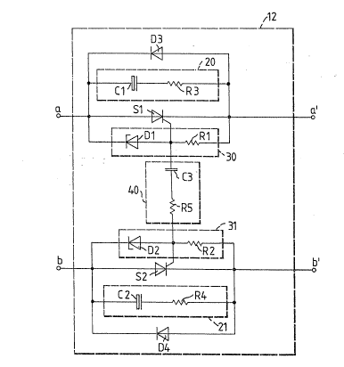
Figure 2 shows a preferred embodiment of a
remote-controlled master switch facility in which
thyristors S1, S2, which are connected into lines ~~A~ (Ila)
and ~-B~ (llb) are being used as switches. In order to
provide polarity independence for the remote-controlled
master switch facility, diodes D3 and D4 are connected
parallel to thyristors Sl and S2, whereby the forward
direction of the diodes D3, D4 is opposed to the forward
direction of the thyristors. In correspondence with the
polarity of the remote-controlled master switch facility,
in one line branch the thyristor takes over current flow
while in the other line the diode does this. If, for
example, core lla of the telecommunication circuit is
positive compared with core llb, during operation the
supply current will flow via thyristor S1 and Diode D4.
~nother possible embodiment o~ the invention is a remote-
controlled master switch facility with triacs. In thiscase diodes D3, D4 are redundant since a triac conducts
~3S~
current in hoth directions. The bridying paths 20, 21 are
connected parallel to the switches. The voltage-dependent
turn-on characteristics of thyristors S1, S2 is achieved
through the implementation of the control branches 30, 31.
To achieve rapid response for the thyristors S1, S2 during
pulse dialling, both control branches are connected via a
coupling device 40.
In the pulse dialling method, dial pulses are
generated in the telephone 14 by way of a dial pulse switch
within the telephone which opens and closes in the
frequency of the pulses. When the dial pulse switch is
closed, current must flow so that the dial pulses can be
recognized by the exchange 10. Consequently, the
corresponding thyristor of the remote-controlled mastar
switch facility 12 must be closed during a dial pulse to
allow the current to flow. When the dial pulse switch
within the telephone opens, the thyristor will also open
since the retaining current is underflowed. The thyristor
must close approximately every 100 milliseconds. When
there is no coupling device 40, this rapid closing of the
thyristor is prevented by the capacitor in the bridging
path, because, during the previous pulse, the capacitor was
discharged via the conducting thyristor and can not
recharge to the breaking voltage during the 30-40
milliseconds that the dial pulse switch is open. Due to
the high-impedance telephone, the time constant for
charging the capacitors C1, C2 in the bridging path 20, ~1
is somewhere in the range between 20 and 100 milliseconds.
The time constant for thP coupling device 40 is smaller
than 10 milliseconds so that the capacitor C3 of the
coupling device 40 can supply the trigger pulse for the
thyristor S1, S2 when the dial pulse switch in the
telephone closes. The coupling device 40 thus utilizes
the charging current of the capacitors Cl, C2 which arises
after the dial pulse switch opens, whereby part of this
current is stored in the capacitor C3 of the coupling
2 1~ ~3 r3 ~
device ~0 and is thus available as trigger energy for the
thyristors when the dial pulse switch closes again.
Figure 3 illustrates the behaviour of the remote-
controlled master switch facility, both with the coupling
device 40 (broken line) and without the coupling device 40
(solid line), for pulse dialling. In ihis example, the
potential of core lla is positive with respect to the
potential of core llb. Figure 3(I) shows the conditions
for the dial pulse switch within the telephone 14, Figure
3(II~ shows the charge voltage at capacitor Cl of the
bridging path 20 as a function of time, Figure 3(III)
represents the loop current as a function of time and
Figure 3(IV) shows the current in the coupling device.
If the circuit is operated without the coupling
device, then prior to the first dial pulse 50, capacitor Cl
is charged up to the breaking voltage determined by diode
Dl. The thyristor Sl can then fire and a constant loop
current 70 then flows for the duration of the pulse.
Following the dial pulse 50, the capacitor Cl slowly
recharges. However, the time constant is very high because
the impedance of the telephone between pulses can range
between 100 K-Qhms and several M-Ohms. Thus, at the
beginning of the next dial pulse 51, the capacitor voltage
61 will not as yet have reached the breaking voltage level
and the thyristor Sl can not be fired. During the pulse
51, an increased charging current 71 flows because during
the period of a dial pulse the telephone becomes low-
impedient (typically around 300 Ohms). Due to the
increased charging current, the voltage on the capacitor
Cl, ~2 increases correspondingly rapid. At the beginning
of the third pulse 52~ the voltage will not as yet have
reached the breaking voltage, sc that the thyristor Sl does
not fire at the beginning of the pulse but at some later
point 72. Due to the discharge of the capacitor C1, the
condition for the fourth pulse corresponds to the condition
during the second pulse 51.
; '
,-
2 ~
The behaviour of the circuit with a coupling
devic~ 40 is shown in Figure 3 (I) through (IV) with the
broken line. For the first pulse 50, the thyristor Sl will
fire because of the charge voltage of the capacitor Cl .
For the second pulse 51, the charge voltage is not
sufficient for the thyristor to fire. The trigger pulse 80
is thus supplied by the coupling device 40 which charged up
between pulses.
Figure 4 shows a preferred embodiment of the
invention in which the switches 12a, 12b are implemented
with MOS~FETs. The MOS-FET switch 12a includes the two
MOS-FET branches 100, 101 while the MOS-FET switch 12b is
formed by the MOS-FET branches 102, 103. In this
embodiment, the MOS-FET branches 100, 103 incorporate p-
channel MOS-FETs and branches 101, 102 incorporate n-
channel MOS-FET. Each MOS-FET branch consists of a MOS FET
pair (Ql, Q2), (Q3, Q4), (Q6, Q7) and (Q8, Q9) whereby in
each case the gate and source terminals of a MOS-FET pair
are connectad. The channel substrate diodes are connected
in opposition to each other so that the current can only
flow between the subscriber and the exchange via the MQS
transistor channels. It is also conceivable to connect the
drain terminals with each other instead of the source
terminals, to prevent the current from flowing via the
substrate diodes. The p-channal branches 100, 103
respectively take the current which flows to the
subscriber, while the n-channel branches 101, 102 take over
the current flowing from the subscriber to the exchange.
Since each switch 12a, 12b has both an n-channel as well as
a p-channel, the circuit operates independent of polarity.
Control for the MOS-FET branches 100, 101, 102
and 103 i5 implemented via one voltage divider each (Rtl,
Rt8~, (Rt2, Rt7), (Rt3, Rt6~, (Rt4, Rt5). The resistance
Rt8 of the voltage divider for branch 100 can be bridged by
a MOS FET Q5 with a serial resistor Rsl and a diode Dsl.
The gate of the controlling MOS-FET Q5 is driven by the
2 ~ ~ ~3 ~
11
voltage divider ~s2, ~s3. The same applies for branch 103;
here a controlling MOS-FET Ql0 with a serial re~istor Rs4
and a diode Ds2 bridge resistor Rt5 in the through-
connected state of the MOS-FET. The gate of Q10 is wired
up with a voltage divider comprising resistors Rs5 and Rs6.
For voltage limitation purposes, æener diode pairs Zl, z2,
Z3 and Z4 are wired up between the source and base lines of
the respective hranches 100, 101, 102 and 103. The same
applies for MO~-FETs Q5 and Ql0, where zener diode pairs Z6
and Z3 are used. The wiring and the voltage divider are
dimensioned such that a high turn-on voltage and a low
turn-off voltage are obtained. The turn-on voltage may be
a few volts below the supply voltage of the
telecommunication network while the turn-off voltage may be
l~ below 10 volts. This circuit arrangement takes into
account that when low-impedance terminal equipment is put
into operation, the voltage drops well below the turn-on
threshold of the remote-controlled master switch facility.
The controlling MOS-FETs Q5 and Q10 produces hysteretic
behaviour in the switching threshold for the n-channel
branches 101 and 102. The capacitors CGl through C~4,
which are wired between the source and gate lines of
branches 100, 101, 102 and 103, cause a delayed turn-off of
the MOS-FETs and thus facilitate the transmission of AC
ringing currents.
Figure 5 shows a simplified circuit section of
the circuit illustrated in Figure 4, and the accompanying
wiring to the exchange side and the subscriber side.
Figure 5 is used to explain the mode of operation o~ the
circuit shown in Figure 4 Put simply, the exchange is
represented as a DC voltage source Vamt and two resistors
Ra and Rb which represent the supply resistances and line
resistances for each core lla and llb. In this simplified
description, the telephone on the subscriber side is
represented as a cradle switch GU and a resistor Rtel.
When the cradle switch is open, i.e. the receiver is hung
320~
12
up, the full supply voltage Vamt is available to the
subscriber ~nd thus also to the input of the remote-
controlled master switch facility, since resistors Ra and
Rb are small comparsd with the insulation resistance of the
telephone. When the cradle switch G~ is closed, the
telephone 14 is low impedient and resistors Ra, Rb and Rtel
form a voltage divider, whereby, depending on the line
length, only 15 to 30% of the exchange voltage Vamt reaches
the telephone 14. The switching threshold of the remote-
controlled master switch facility must thus be not higherthan this limit, and, for an exchange voltage Vamt of 60V,
would be 9V. However, in test situations it is desirable
to be able to perform measurements with voltages between 10
and 20 V, without the subscriber being connected. This is
not possible in conjunction with a simple switching limit
of 9V. ~ control circuit is thus required which provides
a high turn-on threshold and a low turn-off threshold, i.e.
one which exhibits hysteretic behaviour. The two MOS-FETs
Ql and Q2 which are serially wired into the subscriber line
lla, (with their respective source and gate terminals
connected with each other) lead the current to the
telephone 14 in the switched-on condition. The control for
branch 100 (comprising Ql and Q2), is implemented through
voltage divider Rtl and Rt8. These two resistances
determine the turn-on threshold of the circuit and can be
placed, for example, at 50% of the exchange voltage (supply
voltage). Thus the turn-on voltage is considerably higher
than the voltage which would by available at the input of
the remote-controlled master switch facility while the
cradle switch GU is closed. If the turn-on threshold is
exceeded, the MOS-FETs Ql and Q2 are rendered conductive
and the same voltage that is present at the input of the
remote-controlled master switch facility is also present at
the output of the same, i.e. at voltage divider Rs2, Rs3.
The voltage divider Rs2, Rs3 is dimensioned in such a way
that, for small voltages of approximately 15 to 20% of the
13
exchanga voltage, the n-channel MOS~FET Q5 is conductive.
In this condition, the high-impedance resistor Rt8 is
bridged by thP low-impedance resistor Rsl. The consequence
of this is that, even if the cradle switch GU is closed,
the MOS-FETs Ql and Q2 remain conductive even for small
voltages. Since the MOS-FETs can be practically
powerlessly controlled, the voltage divider resistances can
be kept very high, i.e. in the ~-Ohm range, so that the
power consumption of the circuit is very small.
Figure 6 shows a simplified schematic diagram of
an embodiment of the invention in which a single MOS-FET is
used in each of the branches 100, 101, 102 and 103 instead
of a MOS-FET pair, respectively. Switches 12a and 12b
consist o~ one n-channel (Ql, Q~) and one p channel (Q3,
Q6) MOS-FET, which are connected in parallel in such a way
that the anodes of the substrate diodes are wired towards
the subscriber. In this case the substrate diodes of the
MOS-FETs can only conduct current from the subscriber to
the exchange. That is why the switching threshold for the
return flow branch is not greater than 0.6V. Otherwise the
circuit design corresponds to the embodiment according to
Figure 4.
Figure 7 shows a further preferred embodiment of
the invention, wherein the control circuits for the
branches are diagrammatically represented as blocks 160 and
161, and correspond to that shown in Figure 4. The n-
channel MOS-FET branches 101 and 102 of the circuit shown
in Figure 4 can be left out if the p-channel branches 100
and 103 are each controlled by a DC/DC converter 150, 151
in addition to the above described control circuits 160,
161 which cause tha hysteretic behaviour. The converters
150, 151 generate a negative voltage when the correspondiny
p-channel pair 100, 103 is in the negative branch of the
telecommunications line and conducts current from the
terminal equipment to the exchange. A complementary
circuit with n-channel switches and DC/DC converters, which
1~
generate a positive potential for the n-channel switch
which is in the positive branch, is also conceivable.
Figure 8 shows a remote-controlled master switch
facility with controlled silicon rectifiers, and represents
a modified version of the circuit shown in Figure 2. The
electrollic switch 12b in core b is reverse poled to switch
12a. Thus the forward direction of diodes D2 and D4 and
thyristor S2 is antiparallel to that of diodes D1 and D3,
and thyristor Sl in core a. When core a has a positive
voltage with respect to core b, thyristors Sl and S2 ars
inhibited if the measurement voltage is below the switching
voltage. When the measurement voltage is neg~tive, diodes
D3 and D4 become conductive and the subscriber side is
included in the measurement process, i.e. switches 12a and
12b are switched back on again.
Figure 9 shows a correspondingly modified ~OS-FET
circuit from Figure 6. In this case the MOS-FET
transistors in core b are interchanged. Transistor Q6 is
now an n-channel type and transistor Q8 is a p~channel
type. On the other hand, in the circuit according to
Figure 6, the switches are symmetrical. Furthermore, the
respective Schmitt trigger transistor Q10 of the
corresponding control has been replaced with the
complementary p-channel type.