Note: Descriptions are shown in the official language in which they were submitted.
20832 1 6
ELECTRICAL ENERGY METER WITII A PRECISION
IN'rEGRATOR FOR CURRENT MEASUREMENT
BACKGROUND OF THE INVENTION
This invention relates to circuits an~ methods for
measuring electrical energy, and more particularly to
electrical energy measurement circuits and methods involving
current sensors of the type which generate a signal
proportional to the derivative of a current with respect to
time (di/dt).
Meters for measuring electrical energy conventionally
measure current and voltage on the metered power line and
multiply the measured current and voltage to produce a signal
representative of the electrical power consumed by a load
connected to the metered power line. One known way of
measuring electrical current is witll an inductive current
pickup, which produces a signal proportional to di/dt.
Current sensors of this type have been referred to as mutual
inductance transformers, mutual inductance current
transducers, and embedded coils, and are described, for
example, in the following patents:
Patent No. Inventor Issue Date
3,226,641 Miller Dec. 28, 1965
4,182,983 Heinrich et al. Jan. ~, 1980
4,250,552 Elrlls Feb. 10, 1981
4,368,424 Miller Jan. 11, 1983
4,473,810 Souques et al. Sep. 25, 1984
4,591,810 Mackenzie et al. May 27, 1986
4,596,951 Heinrich et al. Jun. 24, 1986
5,053,697 Carnel et al. Oct. 1, 1991
28201-6
~A
20832 1 6
Because the output of the embedded coil or other
inductive current pickup is a voltage proportional to the
derivative of the load current, the current sensor output
must be integrated to obtain a signal proportional to the
load current. This general concept is illustrated in FIG. 1,
and various forms of integrators are disclosed in the
above-referenced patents.
Ideally, an inductive current picl~up exhibits a yhase
shift of precisely 90~, which can be offset by a simple
integrator circuit consisting of a cayacitor in the feedback
loop of an operational amplifier (op amp). A basic
integrator of this type is shown in the Mackenzie patent
referenced above, in which a second integrator having its
input connected to a square-wave clock signal is also
employed, with the outputs of the two integrators being added
together an~ supplied to a comparator which generates a
pulse-width-modulated (PWM3 signal having a duty cycle
proportional to metered current. A negative feedback path
including a low-pass filter is connected between the
comparator output and the input to the basic integrator to
compensate for errors produced by the integrator and
comparator, thus, according to the patent, permitting the use
of low-cost inverter circuitry fabricated on an integrated
circuit. A similar configuration is disclosed in U.S. Patent
No. 4,596,951 to Heinrich et al., in which one form of the
pulse-width modulator includes a capacitor and a plurality of
resistive components in the feedback network of an op amp,
along with a bypass capacitor connected to the negative
regulated reference voltage supply and one of the resistive
components in the feedback network.
An integrator with a parallel resistor-capacitor (RC)
network in the feedback loop of an op amp connected to a
di/dt sensor is disclosed in U.S. Patent No. 4,182,983 to
Heinrich et al., which also relates to a PWM technique.
. ..
~' A
28201-6
3~6
-3-
A similar integrator circuit is shown in U.S. Patent No.
4,250,552 to Elms, in which the output of the integrator is
connected to a twin-T network.
U.S. Patent No. 5,053,697 to Carnel et al. discloses an
op amp integrator having multiple capacitors in a feedback
network including a resistor connected to the op amp
inverting input and a resistor directly connecting the op amp
output to its noninverting input. The circuit also includes
a passive RC filter of the integrator type connected upstream
from the two inputs to the op amp, for the stated purpose of
compensating for a difference between the phase shift
imparted by the active filter and a predetermined value
desired for said phase shift.
U.S. Patent No. 3,226,641 to Miller shows a bridged-T
network in the feedback path of an amplifier, the bridge-T
network including a capacitor and a T network consisting of
two resistors in series, with the common leads of the
resistors connected to ground through a second capacitor. A
third capacitor is connected in parallel with an input
resistor to compensate for secondary inductance of the
current transformer.
The actual phase shift exhibited by an inductive current
pickup is not precisely 90~ due to eddy currents set up in
the conductors exposed to the magnetic field and eddy
currents in the magnetic material in the flux path.
Therefore, an integrator exhibiting a phase shift of
precisely 90~ is not necessarily the solution to the problem
of converting the inductive pickup output signal to a signal
proportional to current. Although a desired small deviation
from 90~ phase shift in the integrator can be achieved by
setting the corner frequency of a first-order low-pass filter
to a sufficiently low frequency, e.g., under 1 Hz for a
desired phase deviation on the order of 0.5~, it has been
found that some undesirable trade-off is usually required,
either in the form of a resistance value which is excessively
~:)83;~
--4--
high for a desired specification of DC offset, or because the
required capacitor is either too large in size, too sensitive
to temperature, or more expensive than desired in the
increasingly cost-sensitive market for watthour meters and
the like.
Thus, there remains a rleed, in electrical eneryy meters
of the type having a di/dt current sensor, for an improved
integrator design offering stability with time and
temperature, linear performance, low DC output voltage, low
sensitivity to component tolerances and frequency variations,
low component count, and compensation for nonideal phase
characteristics of embedded coils and the like.
-5- ~ 6
SUMMARY OF THE INVENTION
The present invention provides an improved circuit for
electrical energy measurement which includes a current sensor
for generating a first signal proportional to the derivative
of a current with respect to time in an electrical power line
having a nominal line frequency, whicll is, for exarnple, 60 I-{z
in the United States and 50 Hz in Europe, the current sensor
having a nonideal phase characteristic including a phase
deviation from 90~ at the nominal line frequency. An
underdamped integrator integrates the first signal,
compensating for the phase deviation in the nonideal phase
characteristic of the current sensor. The integrator has a
transfer function with a magnitude peak at a frequency below
the line frequency and with a phase shift deviating from 90~
at the line frequency.
A general object of the present invention is to provide
an improved electrical energy measurement circuit of the type
having an inductive current pickup and an integrator for
generating a signal proportional to current in a metered line.
Another object is to provide an integrator capable of
compensating for the nonideal phase characteristics of real
inductive current pickups.
Another object is to provide low sensitivity,
particularly low sensitivity of phase shift, to component
tolerances and variations in frequency from the nominal line
frequency.
Yet another object of the invention is to provide low
sensitivity to component tolerances and frequency variations
while maintaining low parts count and cost without
sacrificing stability with respect to time and temperature.
Through a novel combination of elements as recited in the
claims, the present invention provides a low-cost integrator
design having stability with time and temperature, linear
performance, low DC output voltage, low sensitivity to
;~83~16
component tolerances and frequency variations, low component
count, and compensation for nonideal phase characteristics of
embedded coils and the like.
These and other objects and advantages of the present
invention will become more apparent upon reading the
following detailed description in conjunction with the
accompanying drawings.
~~~ 3L6
BRIEF DESCRIPTION OF THE DRAWINGS
FIG. 1 illustrates the general concept of a di/dt sensor
coupled to an integrator in order to produce an output
voltage proportional to the line current.
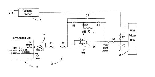
FIG. 2 is an electrical schematic of an embedded coil and
precision integrator according to the preferred embodiment of
the present invention.
FIGS. 3 and 4 are plots of the closed-loop gain and
phase, respectively, of the integrator of FIG. 2.
-8- 208321 6
DESCRIPTION OF T~E PREFERRED EMBODIMENT
For the purposes of promoting an understanding of t~le
principles of the invention, reference will now be made to
the embodiment illustrated in the drawings and specific
language will be used to describe the same. It will
nevertheless be understood tllat no limitation of the scope of
the invention is thereby intended, such alterations and
further modifications in the illustrated device, and such
further applications of the principles of the invention as
illustrated therein being conteMplated as would normally
occur to one skilled in the art to which the invention
relates.
FIG. 1 illustrates the general con~iguration of a current
measurernent circuit in a watthour meter or the like such as
described above in which measured current is multiplied by
measured voltage (circuit not shown) to produce a signal
representative of the power consumed by the load at any given
time. In the preferred embodiment, an ernbedded coil 10 is
connected in series with a load connected to an electrical
power line, as shown in FIG. 1, and the secondary winding of
the embedded coil is connected to an integrator 20.
-
Referring to FIG. 2, the embedded coil in the preferredembodiment produces an output voltage of 1.6S volts RMS on
its secondary winding in response to a primary current o~ 200
amps, and typically has a lKQ source resistance (Rs).
The secondary winding of the embedded coil is connected on
one end to signal ground and on the other end to the input of
integrator 20 as shown in FIG. 2, with the coil windings
connected in a known fashion such that the embedded coil
output voltage, as measured between the integrator input and
signal ground, is out of phase with the primary current by
28201-6
~)83~6
g
approximately 90~. A typical phase shift for an actual
embedded coil is 90.12~. In one embodiment, integrator 20 is
designed to produce a phase shift of 90.12~ at 60 Hz so as to
precisely offset the phase lag of the embedded coil.
However, integrator 20 is preferably designed to produce a
phase shift of 90.41~ at 60 Hz so as to more than offset the
phase lag of the embedded coil and produce a phase angle for
the integrator/coil combination which falls between the phase
angle of the measured voltage input with minimum power factor
(PF) adjustment and the voltage input phase angle with
maximum PF adjustment. Power factor adjustment is performed
by introducing a phase shift in the voltage measurement
circuit (not shown) and is intended to adjust the phase angle
of the voltage input to equal that of the combination of
embedded coil and integrator so that the meter reading will
be correct for the anticipated load power factor. Those
skilled in the art will appreciate that meter errors can be
minimized by designing the current measurement circuit such
that its overall phase angle is at or near the middle of the
range of possible voltage input phase angles as adjusted by
phase shift circuitry provided in the meter for this purpose.
The embedded coil may be connected so as to produce a
phase lead or a phase lag, the principal difference between
the two being a 180~ phase difference which does not affect
the amplitude of the measured current. In multi-phase
systems, errors in other parts of the system can be cancelled
or reduced by means of such differences in polarity between
embedded coils for different phases of the power line.
Integrator 20 includes a resistive input consisting of a
magnitude calibration (Mag cal) potentiometer 22 and two
resistors, Rl and R2, connected in series between the
embedded coil and the inverting input of a TL081I op amp 24.
Between the output and inverting input of the op amp a
bridged-T network is connected including a T network,
consisting of resistors R3, R4 and R5 and capacitor C4, and a
bridging capacitor C3, all connected as shown in FIG. 2. The
-lO- 20832 t 6
op amp is connected to a power supply and its noninverting
input is connected to signal ground, as shown in FIG. 2. The
output of the integra~or is app1ied t~lrough a resistor ~6 to
a watt trans~ucer chip or integrated circuit of the type
disclosed in U.S. Patent No. 4,896,106, for time division
multiplication.
Although the integrator output may, if desired, be
applied to the input of an amplitude modulator which is
contained in the watt transducer chip, with the voltage
signal for the corresponding power line applied to the
mark-space oscillator in tl~e watt transducer chip, as
disclosed in the aforementioned U.S. Patent No. 4,896,106,
the integrator output is pre~erably connected througll R6 to
the mark-space oscillator input and the voltage measurement
signal is supplied to the amplitude modulator input, in order
to reduce the effect of input DC offset voltage which could
lower the dynamic range and thereby produce larger meter
registration errors at the low end of the load curve. The
preferred values of R7 and C5 at the mark-space oscillator
input are as listed below. The current signal produced by
integrator 20 may alternatively be multiplied by or combined
with the voltage measurement in a number of different ways
known to those skilled in the art, although the preferred
technique is time division multiplication, which is described
in further detail in 'he above-referenced U.S. Patent No.
4,896,106.
In the preferred embodiment, the values of the
above-referenced components are as follows:
Component Value
Mag cal pot0-105 KQ
Rl 205 KS2
R2 lS9 KS~
R3, R4 1 MQ
R5 33.2 KS2
R6 49.9 KQ
R7 100 KQ
C30.012 ~F, NPO ~5~
C40.1 ~F, X7R ~10%
C5 0.033 ~F
28201-6
~3~'~L6
--11--
At least resistors Rl-R5 are MIL type RN55C resistors,
which have +1.0% tolerance and a specified temperature
coefficient of 50 ppm/~C. The op amp has a JFET input, which
is preferred in order to minimize the effect of input bias
and offset currents. Resistors R3 and R4 are preferably held
to values no greater than lM in order to keep DC offset
within acceptable limits, although it is contemplated that
higher values of R3 and R4 and different values of other
components may well be acceptable in certain applications and
in certain meter designs.
The closed-loop gain and phase of the integrator
corresponding to the above-listed values are plotted in FIGS.
3 and 4, respectively, which correspond to the following
closed-loop transfer function of integrator 20:
G = -k s + 18.75
s2 + 21.35s + 781.4
where k varies with the Mag cal pot setting ~Rcal).
In more general terms, the transfer function of the
disclosed integrator takes the following form:
-
s +
RirlC3 s2 + s ( 1 3) + _ _ _
where Rin = Rs + Rcal + Rl + R2
Tl = (R3 + R4) C3
T2 = (R5 + R3//R4) C4
T3 = (R5)(C4)
With the component values specified above, integrator 20
exhibits an underdamped response with an undamped natural
frequency of 4.5 Hz and a damping factor ~ = 0.38. Taking
both the numerator and denominator terms of the transfer
~8~ 6
function into account, a magnitude peak occurs at 4.2 Hz,which lies between one and two orders of magnitude or decades
below the nominal line frequency of 60 Hz (U.S. standard).
Most preferably, the peak occurs at approximately 1/15th of
the nominal line frequency, whether it be 60 Hz in the United
States or 50 Hz elsewhere. The resulting sensitivity to
variations of frequency and to component tolerances is as
specified below:
Variation of Frequency (60Hz %5%)
10 Freq. (Hz) Gainl Phase2 Error (%)3 Error (%)4
57 1.00320 90.43~ 0.32 0.06
60 1.00000 90.41~ 0 0
63 0.99808 90.39~ 0.19 0.06
Sensitivity to Component Tolerances
Condition Gainl Phase2Error (%)3 Error (%)4
WCase (max) 1.06432 90.45~ 6.43 0.12
Nominal 1.00000 90.41~ 0 0
WCase (min) 0.94223 90.38~ 5.78 0.09
1 Gain of the integrator/embedded coil combination,
normalized with respect to nominal conditions (60 Hz or
nominal component values)
2 Phase of the integrator phase
3 Meter registration error due to nonideal rnagnitude
performance of the integrator at PF = 1.0
4 Meter registration error due to nonideal phase performance
of the integrator at PF = 0.5
Meter registration error = VI~cosr'
where I = actual current value
r = actual phase angle between voltage and
current
I' = measured current value
r' = measured phase angle between voltage and
current.
Z083;~1~
-13-
As an example illustrating the above for a power factor
of 0.5, which is known to correspond to a phase angle of 60~,
the phase characteristic of the integrator results in a phase
error of 0.02~ for a 5% variation in frequency, as indicated
in the above table. With all other variables unchanged,
actual current and voltage equal measured current and voltaye
such that the equation for meter registration error reduces
to the following:
lo cos 68 02~ = 0.9994 (-0.06%)
While the component values specified above are
particularly advantageous for an ernbedded coil exhibiting a
phase lag of 90.12~, it will be readily appreciated by those
skilled in the art that substantially similar performance can
be achieved by applying the foregoing general principles to
embedded coils and other types of inductive current pickups
having different phase characteristics or other nonideal
characteristics.
In order to minimize the sensitivity of the inverting
input node of the TLO81I op amp to stray capacitive fields,
such as due to capacitive coupling from line potential on the
potential transformers, power supply transformer and embedded
coil primary blades, the integrator circuit layout on the
printed circuit board preferably has rninimum lead/trace
lengths around the op amp inverting node, and electrostatic
shielding is also preferably provided around the inverting
node. For ease of construction, it is suitable to place an
electrostatic shield over the entire op arnp circuit.
Althouyh described above in terrns of an analog inteyrator
with a single op amp, the integrator function may
alternatively be performed using state-variable techniques
with multiple op amps, or may be implemented digitally, i.e.,
with a microprocessor or other prograrnmable digital logic
containing an algorithm corresponding to the integrator
2083;~1fi
-14-
transfer function and having an input connected to the
embedded coil via an A/D con.verter.
While the invention has been illustrated and described in
detail in the drawings and foregoing description, the same is
to be considered as illustrative and not restrictive in
character, it being understood that only the preferred
embodiment has been shown and described and that all changes
and modifications that come within the spirit of the
invention are desired to be protected.