Note: Descriptions are shown in the official language in which they were submitted.
~0~3237
STACKED TERMINATION RESISTANCE
BACKGROUND OF THE INVENTION
1. Field of the Invention
This invention relates to electrical resistance components, and more
particularly to an electrical resistance component of the type conventionally
used
for termination of a data bus cable.
2. Description of Related Art
It is well known to use resistance elements for the purpose of terminating
a data bus cable. The use of resistance elements at the termination of the
data bus
line prevents reflection of energy back up the line by providing a load
impedance
which matches the characteristic impedance of the line, thus permitting
transmission of high frequencies with a minimum of loss. Conventionally, such
termination resistances are formed from resistor chips bonded to wires of the
cable
208323'
2
by direct soldering of the wires to slots in the chips. The wires arp prepared
by
stripping the cables and pre-tinning the wires to form leads suitable for
supporting
the resistor chips.
Such conventional cable termination arrangements are subject, however, to
axial misalignment of the stack of resistor chips, and to separation of the
cables
and leads from the chips. Although numerous different arrangements are
presently
used for stacking and aligning resistance elements in contexts other than
cable
termination, none has proved completely satisfactory in the specific context
of
cable termination.
Furthermore, in addition to the problems of misalignment and lack of
mechanical integrity, conventional stacked termination resistance components
often lack shielding and environmental sealing arrangements suitable for use
in the
context of data bus termination. Current packaging arrangements have tended to
be both unwieldy and excessively costly to manufacture.
SUMMARY OF THE INVENTION
The present invention seeks to provide an alternative to direct soldering of
cable leads to slots in cable termination resistance elements and an
alternative to
using stripped and pretinned wires of the cables themselves as the conductors
to
which the resistor chips are electrically bonded.
To accomplish these objectives, the invention calls for the formation of
precision plated through-holes in a stack of resistor chips, the through-holes
2083237
3
providing an electrical and structural interface between the conductors and
the
chips.
In the alternative embodiment of the invention, the conductors include
conductive rods which are used in place of conventional stripped and pretinned
cable leads, the conductive rods being separately bonded to the wires of a
data bus
cable through a variety of known bonding methods.
The present invention also provides an improved packaging arrangement
which offers both an electrical shield and an environmental seal, and which is
implemented in an especially simple and convenient-to-manufacture manner by
eliminating complicated and expensive fixturing while permitting use of
automated
soldering techniques in lieu of hand soldering.
BRIEF DESCRIPTION OF THE DRAWINGS
Fig. 1 is a perspective view of the unassembled parts which make up a cable
termination resistance stack assembly according to the preferred embodiment of
the invention.
Fig. 2 is a cut-away perspective view of a preferred termination assembly
using the parts shown in Fig. 1.
Fig. 3 is a perspective view showing the assembly of Fig. 2.
Fig. 4 is a perspective view of the assembly of Fig. 3, including alternate
additional electrical shielding.
2083237
4
Fig. 5 is a perspective view of the assembly of Fig. 3, including an
environmentally protective seal.
Figs. 6-8 are perspective views of alternative chip configurations for the
assembly of Figs. 2-5.
Fig. 9 is a perspective view of the unassembled parts which make up an
alternative resistance stack for the assembly of Figs. 2-5.
Fig. 10 is a perspective view of a resistance stack made up of the parts
shown in Figs. 6 and 9.
Fig. 1 1 is a plan view of another alternative to the assembly shown in Figs.
2-5.
Fig. 12 is a perspective view of a clamping member according to a preferred
alternative embodiment of the invention.
Fig: 13 is a perspective view of an end cap according to the preferred
alternative embodiment of the invention.
Fig. 14 is a cross-sectional side view of the manner in which the clamp of
Fig. 12 is used in connection with a shell and cable strain relief member.
Fig. 15 is a cross-sectional side view of the end cap of Fig. 13 as used in
connection with a shell.
208323'
Fig. 16 shows a cable or data bus terminated at both ends and including a
potted environmentally protective seal.
DETAILED DESCRIPTION OF THE PREFERRED EMBODIMENTS
In accordance with a first embodiment of the invention, a stacked
5 termination resistance assembly 100 includes a pair of leads 1, the outer
jackets
2 of individual wires of the cable being stripped back, as is best shown in
Fig. 1,
to expose the wires and thereby form leads 1. The leads may be formed from
either single wires or from twisted together and pre-tinned multiple wires of
the
cable.
It will be appreciated, of course, that the invention is applicable to
electrical
transmission lines other than data busses. Termination is a necessity whenever
information is carried by a finite transmission line, whether in the form of
an
amplitude or frequency modulated signal, or encoded pulses. However, the
invention is especially suited for computer system data bus cables.
The ceramic resistor chips 3 which make up stack 101 may have a variety
of configurations, as shown in Figs. 6-8, but each includes a pair of
conductively
plated through-holes or substantially closed openings 4 into which the cable
leads
are inserted, and which function to provide positive alignment between the
individual chips and the leads and to prevent separation of the leads from the
chips.
In order to provide the necessary structural support, the walls of the
openings
should engage the leads over an angle of greater than 180°.
2~8323"~
6
Between the resistor chips 3 are located solder preform washers 5 which
may be cylindrical or comprised of pairs of frustoconical sections, and which
are
threaded onto tho leads 1 to facilitate electrical connection between the
conductive
plating 9 on the openings and the leads.
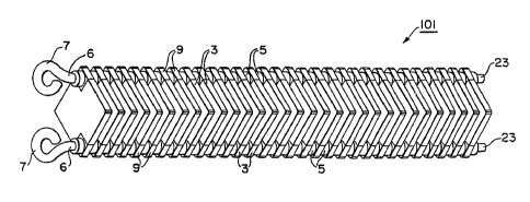
An alternative embodiment of the invention is shown in Figs. 10 and 11.
In this embodiment, instead of pretinned wires, the leads of the resistance
stack
are formed by conductive rods 6. As shown in Fig. 10, the conductive rods 6
include eyelets 7 for facilitating attachment to the wires of a data bus or
cable 8.
The rods may be attached to the cable leads via an electrical bond using such
known welding techniques as laser, electrobond, arc, or percussion welding.
Rods
6 provide a mechanically more secure support for the chips than do the above-
described pre-tinned leads, and simplify the assembly process by eliminating
the
step of pre-tinning, permitting pre-assembly of the resistance stack prior to
attachment of the cable.
As shown in Figs. 1 and 2, the stack termination resistance assembly of the
invention is preferably provided with a tubing shell 10 in the form of a
cylindrical
conductive metallic encasement for mechanical strength and EMI shielding.
Alternatively, shell 10 may be in the form of a non-conductive metal or non-
metallic
encasement for prevention of bending or physical damage, additional EMI
shielding
being optionally applied as described below.
The resistance assembly further includes a non-metallic cylindrical strain
relief clamp 11, which include slots 24 for accommodating cable jackets 2 and
which is depicted for clarity in Fig. 2 as being cut away. Fastening hardware
12
2083237
7
for clamp 11 may include screws with standard slotted heads, as illustrated,
although those skilled in the art will appreciate that a variety of other
mounting
hardware elements may also be used with the preferred strain relief clamping
arrangement.
An end cap 13 with a slotted track 14 is provided for accommodating wire
or conductive rod tips 23 beyond the last resistor chip in the stack. End cap
13
serves to center and parallelly align the cable leads or conductive rods, and
may be
made of the same material as strain relief clamp 1 1. Tapering of end cap 13
may
be added for cosmetic purposes as is best shown in Figure 2.
The termination resistance assembly also includes a flexible strain relief 15
for the wires, attached to clamp 1 1 by a ringlet 16 of heat shrink tubing
material
which is used to increase the shoulder diameter of the strain relief when
additional
shielding and sealing is applied to tubing shell 10 and clamp 1 1. The ringlet
16 of
heat shrink tubing material is secured (heat shrunk) onto the outside of the
flexible
strain relief, filling the diametric gap in transition between the flexible
strain relief
and the clamped set 11. Insulation foam is then preferably injected through a
hole
17 in the shell tubing to insulate the resistor chip assembly from mechanical
shocks. Venting and overflow of the insulation foam are accommodated by
providing a second hole 18 in the shell tubing.
In case the shell tubing is non-metallic, EMI shielding tape 19 is applied
over
the non-metallic shield tubing to offer a full range of electro-magnetic
interference
shielding, as shown in Fig. 4. The shielding tape 19 is overlapped as needed
to
conform to the shape of the cosmetically tapered end cap 13.
2083237
8
Finally, the shielded resistor chip sub-assembly is preferably conformal
coated with an environmentally protective shielding barrier 20, as shown in
Figs.
and 16. In Fig. 16, the shielding barrier has been added to termination
assemblies at both ends of the cable, the strain relief at the second end
being
5 designated by the reference numeral 15' and the second shielding barrier by
20'.
The shielding barriers may be achieved through molding or by applying heat
shrink
tubing with an appropriate adhesive or sealing additive, or lining.
Optionally, the
end of the shielding barrier shrink tubing may be filled beyond the end cap
with high
temperature molding rubber-type compounds 52, and trimmed cosmetically as
shown in Fig. 16.
In order to manufacture the cable termination of the preferred invention,
openings 4 are formed in the chips and precision plated with conductive
material
9. A stack of the prepared resistance elements is inserted over stripped and
pretinned leads 1 or rods 6, with intervening solder preform washers 5.
Washers
5 are then heated to electrically bond the leads or rods to the plating
material 9.
In order to facilitate assembly of the stack, a holder may be used to align
the chips
while the leads are added and soldered.
The preformed stack is then inserted into shell 10, the wires are secured by
clamp 11, ringlet 16, and strain relief 15, and the stack is further secured
and held
in axial alignment by end cap 13, which is attached to shell 10 by any
suitable
mechanical attachment means. Insulation foam is then injected into hole 17,
and
the assembly is subsequently electrically shielded with shielding tape 19 in
the case
of a non-conductive or non-metallic shell. Finally, the assembly is
environmentally
sealed, completing the assembly.
2083237
9
An alternative strain relief clamp 1 1 a and end cap 13a are depicted in Figs.
12-15. In this embodiment, the need for ringlet 16 has beon eliminated by
providing an acceptance cavity 43 in the strain relief clamp 1 1 a. Also,
fastening
hardware 12 is eliminated by the use of an alignment pin 47, and the tube 10
has
been extended to overlap the strain relief clamp 11 a. Tube 10 is held in
place by
rolling material into a groove 46. The end cap 13a has been further modified
to be
held in place by the rolling of material into the groove 31. This embodiment
is
preferred because of the added simplicity resulting from the use of fewer
components. The resistance assembly of Figs. 12-15 includes a non-metallic
cylindrical strain relief clamp 11 a, which includes slots 24a for
accommodating
cable jackets 2, flexible strain relief boot cavity 43 with gripping features
44,
alignment pin hole 45, and staking engagement groove 46.
An end cap 13a with a slotted track 14 is provided for accommodating wire
tips 1 beyond the last resistor chip in the stack. An additional feature used
in
securing the end cap 13a to tubing shell 10 is the staking engagement groove
31
as depicted in Fig. 13.
In this embodiment, the resistance assembly includes bonding of the
interfacial surfaces of the flexible strain relief boot 15 and wire jackets 2,
bonding
of the mating surfaces of the cylindrical clamp halves 11 a and the tracks 24a
in the
clamp 11 a with the wire jackets 2, and bonding of the tubing shell 10 with
the
engagement groove 33 of clamp 11 a. In addition, the interfacial surfaces of
the
engagement groove 31 of the end caps 13a and the inner surface of the tubing
shell 10 are bonded. The assembly of this embodiment is assembled by slip
fitting
and then clamping and staking along the shell's surface at 33 and 33' as
depicted
203237
in Figs. 14 and 15, after which shielding tape 19 and a shielding barrier 20
may be
applied in the manner depicted in Figs. 4, 5, and 16.
It will of course be appreciated by those skilled in the art that numerous
variations of the above-identified embodiments are possible within the scope
of the
invention including, for example, the use of more than two leads or conductive
rods
and uses in contexts other than cable termination and, consequently, it is
intended
that the invention not be limited to the described embodiments, but rather
that it
be limited solely by the appended claims.