Note: Descriptions are shown in the official language in which they were submitted.
2~~~~~rd
DISCHARGE TUBE FOR DISPLAY DEVICE
BACKGROUND OF THE INVENTION
Field of the Invention
The present invention generally relates to discharge
tubes and, more particularly, is directed to a discharge tube
for use with display devices.
Description of the Prior Art
Conventional discharge tubes for use with display devices
will be described hereinafter with reference to FIGS. 1 to 3.
FIG. 1 of the accompanying drawings shows a conventional
DC -plasma display panel (PDP). As shown in FIG. 1, a
plurality of parallel striped cathodes 7 are deposited on a
rear glass panel 6 according to a thick film technique such as
a screen printing or the like. On a front glass panel 1 that
constructs a tube together with the rear glass panel 6, there
are deposited a plurality of parallel striped transparent
anodes (made of ITO (indium tin oxide)) 2 at a right angle
with respect to the cathodes 7. Barrier ribs 12 that prevent
discharge from being spread are deposited on the front glass
panel 1 or on the rear glass panel 6 so as to be located at
each spacing between the adjacent anodes 2 according to the
thick film technique. A discharging gas is sealed into the
tube composed of the front glass panel 1 and the rear glass
panel 6.
FIG. 2 of the accompanying drawings shows a conventional
AC-PDP. As shown in FIG. 2, a plurality of parallel striped Y
1
electrodes 14 are deposited on the rear glass panel 6
according to a thick film technique such as screen printing
and so on or a thin film technique such as vapor deposition,
etching or the like. On the front glass panel 1 that
constructs a tube together with the rear glass panel 6, there
are deposited a plurality of parallel striped X electrodes 13
at a right angle with respect to the Y electrodes 14 according
to the thick film technique such as screen printing and so on
or the thin film technique such as vapor deposition, etching
or the like. The plurality of Y electrodes 14 and the
plurality of X electrodes 13 are respectively covered with
insulating layers 15b, 15a and protecting layers 16b, 16a are
deposited on the insulating layers 15b, 15a, respectively.
The AC type PDP does not need barrier ribs because the
discharge is difficult to be diffused.
FIG. 3 of the accompanying drawings shows a conventional
hybrid-PDP (see Japanese Published Patent Publication No. 3-
76468). As shown in FIG. 3, a plurality of address electrodes
22, 23, each having a self-scanned function based on the DC
discharge, are formed on the rear glass panel 6 to be
intersected at a right angle one another. A semi-AC memory
unit comprises a transparent full electrode 17 disposed on the
front glass plate 1 and which establishes discharge spaces
between it and the address electrodes 22, 23 of the rear glass
panel 6 through a plurality of apertures and a plurality of
aperture metal electrode plate 20 having apertures which are
opposed to the transparent full electrode 17. Insulating
substrates 24 are disposed on each spacing between the
2
2~~3~~~
adjacent address electrodes 22, and the transparent full
electrode 17 is covered with a transparent insulating layer
18. Barriers 19, 21 are respectively disposed between the
aperture metal electrode plate 20 and the transparent
insulating layer 18 and between the aperture metal electrode
plate 20 and the insulating substrate 24. The above elements
thus arranged are sealed into a tube formed of the rear glass
panel 6 and the front glass panel 1 and containing therein
discharge gas.
According to this hybrid-PDP, the electron, generated due
to discharge between the address electrodes 22, 23, is
supplied to the semi-AC memory unit side by a voltage applied
to the aperture metal electrode plate 20 so that AC-discharge
is maintained between the transparent full electrode 17
covered with the transparent insulating layer 18 on the front
glass panel 1 and the aperture metal electrode plate 20. The
hybrid-PDP could simplify a circuit owing to the self-scanned
function thereof and increase a brightness owing to the memory
function thereof.
The conventional DC-PDP shown in FIG. 1 is simple in
structure and is driven to display an image by simultaneously
applying a signal to the plurality of anodes 2 and also by
sequentially applying a ground potential to the plurality of
cathodes 7 in a so-called line sequential driving fashion.
Therefore, the driving of the DC-PDP can be simplified.
However, the above DC-PDP has no memory function so that, if
the number of the anodes 2 and the cathodes 7 is increased in
order to increase a resolution, then a luminous brightness is
3
~~~3~~
lowered. Moreover, the electrodes are short in service life
because a sputtering phenomenon occurs on the electrodes due
to the direct ion bombardment.
The conventional AC-PDP shown in FIG. 2 has a memory
function based on wall charge caused by the fact that electric
charges are accumulated in the insulating layers that cover
the electrodes so that, even if the number of X electrodes and
Y electrodes is increased in order to increase a resolution,
then a brightness can be prevented from being lowered. On the
other hand, a complex signal must be applied between the X and
Y electrodes in order to write, memorize and erase a signal.
Consequently, a driving circuit for the AC-PDP becomes
complicated and a manufacturing process for PDP also becomes
complicated because the operation range must be widened.
The conventional hybrid-PDP shown in FIG. 3 is apparently
complicated i.n structure and hence cannot be mass-produced.
Moreover, this hybrid-PDP suffers from the following
shortcomings and disadvantages.
The diameter of aperture through which the discharge
spaces of the address electrode side and the memory unit side
are coupled must be increased to make the coupling between the
two discharge spaces strong so that the hybrid-PDP can be
operated reliably. If the diameter of aperture is increased
too much, then it is contradictory that the two discharge
spaces cannot be separated reliably. When the memory
discharge is erased, the wall electric charge accumulated on
the insulating layer formed on the transparent electrode of
the front glass panel must be erased. In this case, if the
4
2Q~~~~~
diameter of the aperture on the metal electrode plate is
small, then it becomes impossible to control the wall electric
charge by the address electrode on the rear glass panel side.
Further, if the diameter of the above aperture is large, then
the stable addressing and the self-scanned function are
deteriorated by influences of memory discharge. Furthermore,
the aperture metal electrode plate that isolates the address
side and the display side of the display panel must be exposed
to the gas in order to extract the electrons from the
addressing discharge at the scanning section even though a
part of the metal electrode plate is covered with the
insulating layer or the metal layer is formed on an insulating
body instead of the metal plate. Accordingly, due to the
insulation of the aperture metal electrode plate from the DC-
scanning section and the safe operation, the elements must be
separated with high accuracy one another from a structure
standpoint, which makes the manufacturing process of the
hybrid-PDP more difficult. In addition, since the above
hybrid-PDP operates in a semi-AC fashion, the wall electric
charge that contributes to the memory function is accumulated
only in the address side. Therefore, the memory function is
not powerful and the hybrid-PDP needs a high voltage to
maintain the memory function.
OBJECTS AND SUMMARY OF THE INVENTION
Therefore, it is an object of the present invention to
provide an improved discharge tube for use with a display
device in which the aforesaid shortcomings and disadvantages
encountered with the prior art can be eliminated.
~~.~J~~~~.'~
More specifically, it is an object of the present
invention to provide a discharge tube for use with a display
device which is simple in structure.
Another object of the present invention is to provide a
discharge tube for use with a display device which can be
mass-produced satisfactorily.
Still another object of the present invention is to
provide a discharge tube for use with a display device which
can increase a resolution.
A further object of the present invention is to provide a
discharge tube for use with a display device which can be made
large in size.
Yet a further object of the present invention is to
provide a discharge tube for use with a display device which
can be driven with ease.
Yet a further object of the present invention is to
provide a discharge tube for use with a display device in
which a driving circuit thereof can be simplified in
structure.
Still a further object of the present invention is to
provide a discharge tube for use with a display device which
can be made inexpensive.
According to a first aspect of the present invention,
there is provided a discharge tube for display which comprises
a pair of memory elements, each including a memory electrode
formed of a conductive layer having a plurality of apertures
arranged in an XY matrix form and in which the whole surface
of the memory electrode is covered with an insulating layer,
6
the pair of memory elements being laminated each other such
that corresponding apertures covered with the insulating
layers are communicated with each other to form discharge
cells, and a tube body into which the pair of memory elements
are sealed and into which a discharging gas is sealed, wherein
an AC voltage necessary for maintaining a discharge is applied
between the memory electrodes of the pair of memory elements.
According to a second aspect of the present invention,
there is provided a discharge tube for display which comprises
a pair of memory elements, each including a memory electrode
formed of a conductive layer having a plurality of apertures
arranged in an XY matrix form and in which the whole surface
of the memory electrode is covered with an insulating layer, -
the pair of memory elements being laminated each other such
that corresponding apertures covered with the insulating
layers are communicated with each other to form discharge
cells, a plurality of parallel striped first and second
address electrodes being disposed at a predetermined interval
so as to cross each other, the pair of memory elements
laminated each other being disposed between the plurality of
first and second address electrodes such that respective
crossing points of the first and second address electrodes
correspond to the respective discharge cells, and a tube body
into which the first and second address electrodes and the
pair of memory elements are sealed and into which a
discharging gas is sealed, wherein a predetermined voltage is
applied between the first and second address electrodes
selected from the plurality of first and second address
7
electrodes to cause a discharge to occur in the discharge cell
located at the crossing point thereof and a predetermined AC
voltage is applied between the pair of memory electrodes to
thereby maintain the discharge.
In accordance with a third aspect of the present
invention, there is provided a discharge tube for display
which comprises a front side memory element including a front
side memory electrode having a plurality of apertures arranged
in an XY matrix form serving as discharge cells, the whole
surface of the front side memory electrode being covered with
an insulating layer, a rear side memory element the whole
surface of which is formed of a conductive layer and the whole
surface of which is covered with an insulating layer, the
front side memory element and the rear side memory element
being disposed in an opposing relation, a plurality of
parallel striped first and second address electrodes being
disposed so as to cross each other, the front side memory
element being disposed between the plurality of first and
second address electrodes such that respective crossing points
of the first and second address electrodes correspond to
respective discharge cells, and a tube body into which a
discharging gas is sealed and into which the plurality o.f
second address electrodes are sealed such that they are
disposed between the front side and rear side memory elements,
wherein a predetermined voltage is applied between the first
and second address electrodes selected from the plurality of
first and second address electrodes to cause a discharge to
occur in the discharge cell located at the crossing point of
8
ti
the first and second address electrodes, and a predetermined
AC voltage is applied between the front side and rear side
memory electrodes to thereby maintain the discharge.
In accordance with a fourth aspect of the present
invention, there is provided a discharge tube for display
which comprises a front side memory element including a front
side memory electrode the whole surface of which is formed of
a transparent conductive layer, the whole surface of the front
side memory electrode being covered with a transparent
insulating layer, a rear side memory element including a rear
side memory electrode the whole surface of which is formed of
a conductive layer, the whole surface of the rear side memory
electrode being covered with an insulating layer, the front
side memory element and the rear side memory element being
disposed in an opposing relation, a plurality of parallel
striped first and second address electrodes being disposed
between the front side and rear side memory elements so as to
cross each other, and an insulating barrier having a plurality
of apertures serving as discharging cells corresponding to
respective crossing points of the first and second address
electrodes being disposed therebetween, and a tube body into
which a discharging gas is sealed and into which the memory
elements, the address electrodes and the insulating barrier
are sealed, wherein a predetermined voltage is applied between
the first and second address electrodes selected from the
plurality of first and second address electrodes to cause a
discharge to occur in the discharge cell located at the
crossing point of the first and second address electrodes and
9
2~~~~~~'~
a predetermined AC voltage is applied between the pair of
memory electrodes to thereby maintain the discharge.
In accordance with a fifth aspect of the present
invention, there is provided a discharge tube for display
which comprises a rear side memory element including a
plurality of first and second memory electrodes arranged
alternately, the whole surfaces of the p7.urality of first and
second memory electrodes being covered with an insulating
layer, a plurality of parallel striped first and second
address electrodes being opposed to the rear side memory
element so as to cross each other, and an insulating barrier
having a plurality of apertures serving as discharge cells
corresponding to respective crossing points of the first and
second address electrodes being disposed therebetween, and a
tube body into which a discharging gas is sealed and into
which the rear side memory element, the address electrodes and
the insulating barrier are sealed, wherein a predetermined
voltage is applied between the first and second address
electrodes selected from the plurality of first and second
address electrodes to cause a discharge to occur in the
discharge cell located at the crossing point of the first and
second address electrodes and a predetermined AC voltage is
applied between the plurality of first and second of memory
electrodes to thereby maintain the discharge.
The above and other objects, features, and advantages of
the present invention will become apparent from the following
detailed description of illustrative embodiments thereof to be
read in conjunction with the accompanying drawings, in which
like reference numerals are used to .identify the same or
similar parts in the several views.
BRIEF DESCRIPTION OF THE DRAWINGS ..
FIG. 1 is a perspective view showing an example of a
conventional DC type plasma display panel (PDP);
FIG. 2 is a perspective view showing an example of a
conventional AC-PDP;
FIG. 3 is a diagrammatic view of a section showing an
example of a conventional hybrid type PDP;
FIG. 4 is an exploded perspective view showing a first
embodiment of the discharge tube for use with a display device
according to the present invention;
FIG. 5 is a diagrammatic view of a section view showing
the first embodiment of the present invention;
FIG. 6 is a perspective view showing a first example of a
memory element used in the first embodiment of the present
invention;
FIG. 7 is a circuit diagram showing a writing operation
of the first embodiment of the present invention;
FIG. 8 is a circuit diagram showing a memorizing
operation of the first embodiment of the present invention;
FIG. 9 is a circuit diagram showing an erasing operation
of the first embodiment of the present invention;
FIG. 10 is a timing chart used to explain operation of
the first embodiment of the present invention;
FIG. 11 is a perspective view showing a second example o.f
the memory element used in the first embodiment of the present
invention;
11
~Q~~~~~
FIG. 12 is a diagrammatic view of a second showing a
second embodiment of the present invention;
FIG. 13 is a diagrammatic view of a section showing a
third embodiment of the present invention;
FIG. 14 is a circuit diagram showing a fourth embodiment
of the present invention;
FIG. 15 is a diagrammatic view of a section showing a
fifth embodiment of the present invention;
FIG. 16 is an exploded perspective view showing a sixth
embodiment of the present invention;
FIG. 17 is a diagrammatic view of a section showing the
sixth embodiment of the present invention;
FIG. 18 is a timing chart used to explain operation of
the sixth embodiment of the present invention;
FIG. 19 is a circuit diagram showing a seventh embodiment
of the present invention; and
FIG. 20 is a diagrammatic view of a section showing an
eighth embodiment of the present invention.
DETAILED DESCRIPTION OF THE PREFERRED EMBODIMENTS
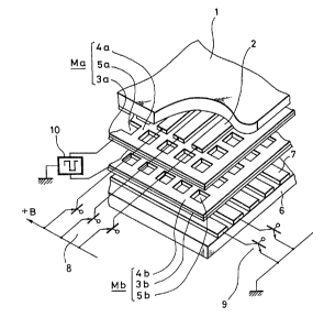
Referring to the drawings in detail, and initially to
FIGS. 4, 5 and 6, a first embodiment of the present invention
will be described in detail hereinafter.
FIG. 4 of the accompanying drawings shows an exploded
perspective view of the discharge tube for use with a display
device according to the first embodiment of the present
invention. FIG. 5 of the accompanying drawings shows a
diagrammatic view of a section thereof and FIG. 6 of the
accompanying drawings shows a perspective view of a memory
12
2~~~~~"~ .
element used in the discharge tube according to the first
embodiment of the present invention. In FIGS. 4 to 6, like
parts identical to those of FIGS. 1 to 3 are marked with the
same references and therefore need not be described in detail.
As illustrated, the discharge tube for display includes a
tube body. This tube body comprises the front glass panel 1
and the rear glass panel 6 whose peripheral edges are sealed
with frit glass and in which the following elements are
accommodated. After the tube body was made vacuous, discharge
gas such as helium, neon, argon, xenon and so on or mixed gas
thereof is sealed into the tube body.
A pair of sheet-like memory elements Ma, Mb respectively
include conductive layers having a plurality of square
apertures 5a, 5b arranged in a two-dimensional fashion or in
an XY matrix fashion, i.e., memory electrodes 3a, 3b formed of
mesh-shaped metal plates that are formed by the metal plate
etching process. The entire surfaces of the memory electrodes
3a, 3b other than the apertures 5~, 5b are covered with
insulating layers 4a, 4b, respectively. The shape of the
apertures 5a, 5b is not limited to a square and other shapes
such as a circle or the like may be used.
The memory electrodes 3a, 3b are each made of metal such
as stainless steel, aluminum, nickel, etc., or alloy of
metals. The insulating layers 4a, 4b are each formed by
sintering at high temperature a paste of glass powder after
being coated on the memory electrodes 3a, 3b according to some
suitable process such as spraying, immersion or the like.
When the insulating layers 4, 4b are made of glass, it is
13
preferable that the memory electrodes 3a, 3b may have
substantially the same thermal expansion coefficient as that
of glass. The insulating layers 4a, 4b may be formed by
oxidizing metal or alloy constructing the memory electrodes
3a, 3b. Furthermore, protecting layers such as magnesium
oxide or the like may be formed on the insulating layers 4a,
4b similarly to the AC-PDP.
The pair of memory elements Ma, Mb of the same shape and
size are laminated each other so that the respective
corresponding apertures 5a, 5b covered with the insulating
layers 4a, 4b are communicated to form discharge cells. Then,
an AC voltage whose amplitude is sufficient to the extent such
that the discharge within the discharge cells can be
maintained is applied across the pair of memory electrodes 3a,
3b from a memory power supply 10.
Memory operation by the pair of memory elements Ma, Mb
will be described below.
When a discharge is excited within the discharge cell due
to the writing of a signal by the discharge between the anodes
2 and the cathodes 7 which will be described later on,
electric charge particles such as ion, electron or the like
within the tube body are attracted into the apertures 5a, 5b
in response to 'the polarity of the memory electrodes 3a, 3b by
the AC voltage applied thereacross and accumulated on the
surfaces of the insulating layers 4a, 4b formed on the inner
surfaces of the apertures 5a, 5b to thereby form a wall
electric charge. Then, if the polarity of the memory
electrodes 3a, 3b is inverted by the AC voltage applied
14
~~~~~~'~
thereacross, then a potential difference between the memory
electrodes 3a, 3b is increased because a voltage based on the
wall electric charge is superimposed upon the applied AC
voltage, resulting in a discharge between the apertures 5a and
5b. This phenomenon is repeated, whereby a discharge within
the discharge cell composed of the apertures 5a, 5b when the
discharge is excited within the discharge cell due to the
writing of the signal is maintained.
When the discharge cell is widened, it is enough to
laminate three memory elements or more. Apertures of memory
elements more than two or 'three must be made coincident but
they are not always the same in shape.
A plurality of parallel striped first and second address
electrodes, i.e., the anodes 2 and the cathodes 7 are disposed
at a predetermined interval so as to cross each other, i.e.,
at a right angle. Between the anodes 2 and the cathodes 7,
there are located the pair of memory elements Ma, Mb which are
laminated such that respective crossing points of the anodes 2
and the cathodes 7 are opposed to respective discharge cells
constructed by the respective apertures 5a, 5b.
Each of the plurality of striped anodes 2 is formed of a
transparent conductive layer such as ITO layer or the like.
The striped anodes 2 are deposited on the front glass panel 1
with the equal width and at the equal interval. These anodes
2 are commonly connected to a positive voltage source +B
through the collectors and emitters of PNP transistors 8 which
are supplied at their bases with signals.
The plura~.ity of striped cathodes 7 are deposited on the
~(~~~~
rear glass panel 6 according to the screen printing and the
sintering process of the conductive paste such as nickel or
the like. These cathodes 7 are grounded via the collectors
and emitters of NPN transistors 9 which are turned on when an
operation pulse is sequentially supplied to the bases thereof.
Since it is sufficient that the trigger-like discharge is
excited between the anodes 2 and the cathodes 7, either or
both of the anodes 2 and the cathodes 7 may be covered an the
insulating layer.
The barrier rib is not always needed. If necessary, the
barrier rib may be disposed on the front glass panel 1 or on
the rear glass panel 6. Alternatively, the barrier rib may be
unitarily formed on a part of the insulating layer of the
sheet-like memory element.
A means for exciting the discharge within each aperture
of the pair of memory elements is not limited to the anodes 2
and the cathodes 7 and other suitable means may be used.
Operation of the above discharge tube for display device
will be described with reference to FIGS. 7 to 10.
As shown in FIG. 7, when a discharge is not yet excited
within the t-.ube body even by the application of pulse voltages
of opposite polarity to the pair of memory electrodes 3a, 3b
as shown in FIG. 10 while the AC voltage having an amplitude
sufficient to maintain the discharge is applied between the
pair of memory electrodes 3a, 3b and the wall electric charge
is not generated within the apertures 5a, 5b covered with the
insulating layers 4a, 4b of the pair of memory elements Ma,
Mb, as shown in FIG. 7, if a switch SWl is turned on for the
16
2~~~~~~
first time and a voltage of 200 V to 250 V is applied to the
anodes 2 through an internal resistance, then a switch SW2 is
turned on and the cathodes 7 are grounded so that a discharge
current flows between the anode 2 and the cathode 7.
Consequently, as shown in FIG. 8, the wall electric
charge is generated in the apertures 5a, 5b covered with the
insulating layers 4a, 4b and the discharge is maintained,
thereby a written display being memorized. At that time, the
switches SW1, SW2 are both turned off so that a bias voltage,
which does not affect the display, is applied to the cathodes
7. Also, the anode 2 is supplied with a voltage that does not
affect the discharge of the anode to which other signal is
being written.
Operation in which the maintained discharge is stopped,
i.e., the memory is erased will be described with reference to
FIG. 9. At the timing in which the negative electric charge
is accumulated in the aperture 5b close to the cathode 7, or
when the positive voltage is applied to the memory electrode
3b, as shown in FIG. 9, the switch SW2 is turned on to apply a
negative erasing pulse to the cathode 7. This negative
erasing pulse inhibits the wall electric charge to be
accumulated in the inner wall of the aperture 5b from being
formed. At the next timing, the discharge is therefore
stopped and the memory is erased.
Another example of the memory element will be described
with reference to FIG. 11. In this example, memory electrodes
3Aa (3Ab) and 3Ba (3Bb) are deposited on both surfaces of a
glass layer 4Ca (4Cb) having a plurality of apertures 5a, 5b
17
arrayed in an XY matrix fashion according to the screen
printing process of the metal plate and the following
sintering process thereof. Thereafter, insulating layers 4Aa
(4Ab) and 4Ba (4Bb) are deposited on the entire surfaces of
the memory electrodes 3Aa (3Ab) and 3Ba (3Bb) by the spraying
process or immersion process of the glass paste, thereby
obtaining the memory elements Ma, Mb.
A second embodiment of the discharge tube for display
according to the present invention will be described with
reference to FIG. 12. In the second embodiment of the present
invention, instead of the sheet-like memory elements Ma, Mb of
the first embodiment shown in FIGS. 4 to 6, the memory
electrodes 3a, 3b and the insulating layers 4a, 4b of the
memory elements Ma, Mb are formed together with the anode 2
and the cathode 7 according to the thick film technique.
There is then the advantage such that the memory elements Ma,
Mb and the anode 2, the cathode 7 can be aligned in relative
position easily and accurately.
A third embodiment of the discharge tube for display
device will be described with reference to FIG. 13. In
accordance with the third embodiment of the present invention,
the diameter of the aperture 5a in the memory element Ma is
made larger than that of the aperture 5b in the memory element
Mb unlike the second embodiment of FIG. 12.
A fourth embodiment of the discharge tube for display
according to the present invention will be described
hereinafter with reference to FIG. 14. The .fourth embodiment
of the present invention is different from the first
18
embodiment of the discharge tube for display shown in FIGS. 4
to 6 such that as shown in FIG. 14, for example, the rear side
memory electrodes 3b is separated to provide a plurality of
rectangular electrodes 3b1, 3b2, ... parallel to a plurality
of cathodes 7, the plurality of cathodes 7 are separated into
groups in association with a plurality of rectangular
electrodes 3b1, 3b2, ... and the electrodes of the same
position at every group of the plurality of cathodes 7 are
connected commonly. As illustrated in FIG. 14, when eight
cathodes 7 are separated into two groups, each having four
cathodes 7 and the memory electrode 3b is separated into two
memory electrodes 3b1, 3b2, it is to be understood that nine
connecting wires for the cathodes 7 and the memory electrodes
3b1, 3b2 are reduced to six connecting wires. A series
circuit of the memory power supply 10 and switches Sa, Sb
which are connected in parallel to each other and which are
alternately turned on and off is connected between the memory
electrode 3a and the memory electrodes 3b1, 3b2.
Generally, when n cathodes 7 are separated, the number of
the connecting wires of the separated memory electrodes 3b1,
3b2, ... and the n cathodes 7 can be reduced to 2 n and
therefore the driver circuits can be reduced considerably.
A fifth embodiment of the discharge tube for display
according to the present invention will be described with
reference to FIG. 15. Operation of the fifth embodiment is
similar to that of the first embodiment shown in FIGS. 4 to 6.
The front side memory element Ma including the front side
memory electrode 3a formed of the conductive layer having a
19
C~ ~ R_I 6d
plurality of apertures 5a arranged in an XY matrix form and in
which the entire surface of the front side memory electrode 3a
is covered with the insulating layer 4a and the rear side
memory element Mb including the rear side memory electrode 3b
the whole surface of which is formed of a conductive layer and
deposited on the rear surface glass plate 6 and the whole
surface of the rear side memory electrode 3b is covered with
the insulating layer 4b are disposed in an opposing relation
to each other. A plurality of anodes 2 deposited on the front
glass panel 1 in parallel to each other and a plurality of '
cathodes 7 deposited on the insulating layer 4b of the memory
element Mb in parallel to one another are disposed so as to
cross each other. The front side memory element Ma is
disposed between the plurality of anodes 2 and cathodes 7, and
a plurality of cathodes 7 are disposed between the front side
and rear side memory elements Ma and Mb.
A sixth embodiment of the discharge tube for display
according to the present invention will be described below
with reference to FIGS. 16 and 17. FIG. 16 is an exploded
perspective view of the sixth embodiment and FIG. 17 is a
diagrammatic view of a section thereof. As shown in FIGS. 16
and 17, in this discharge tube for display, the following
structure is accommodated within the tube bady which is formed
in such a manner that the peripheral edges of the front and
rear glass panels 1 and 6 are sealed by frit glass. The tube
body is made vacuous and then a discharging gas such as
helium, neon, argon, xenon and so on or mixed gas thereof is
sealed into the tube body.
' w
2~8~~~~
The front side memory element Ma and the rear side memory
element Mb are disposed within the tube body in an opposing
relation to each other. The front side memory element Ma
includes the front side memory electrode 3a formed of the
transparent whole surface conductive layer and the whole
surface of the front side memory electrode 3a is covered with
the transparent insulating layer 4a. The rear side memory
element Mb includes the rear side memory electrode 3b formed
of the whole surface conductive layer. The whole surface of
the rear side memory electrode 3b is covered with the
insulating layer 4b. Between the front side and rear side
memory elements Ma, Mb, there are disposed a plurality of
parallel striped anodes 2 and a plurality of parallel cathodes
7 in such a manner that they are crossed each other across an
insulating barrier 11 of a grating configuration having
apertures lla of square shape arranged in an XY matrix fashion
and corresponding to the crossing points of the anodes 2 and
the cathodes 7.
The front side memory electrode 3a is formed of a
transparent whole surface conductive layer such as an SnOz, ITO
or the like. The transparent insulating layer 4a is formed by
the thick film technique in which the pasted glass powder is
printed and baked or by the thin film technique such as the
vapor deposition, sputtering method or the like. The surface
of the transparent insulting layer 4a may be covered with a
protecting film such as an Mg0 or the like. The anode 2 is
deposited on the insulating layer 4a by the printing and
baking of metal pastes such as Ag, Au, A1, Ni or the like
?.1
according to the thick film method or by Cr according to the
thin film method, in addition to the transparent conductive
layer. It is preferable that a width of the anode 2 is made
as narrow as possible in order to generate much more wall
electric charges on the insulating layer 4a that constructs
one portion of the discharge cell of the memory element Ma.
The memory electrode 3b is formed on the rear glass panel
6 according to the thick film method or thin film method. It
is desirable that the cathode 7 is made of a material which
has a low work function and an anti-ion impulse property
similarly to the DC-PDP such as Ni, Labb or the like. Upon
address operation, the cathode 7 is operated at a small
current as compared with the ordinary DC-PDP so that the
material forming the cathode 7 is not limited thereto and a
range in which the material is selected for the cathode 7 can
be widened. Also, it is preferable that a width of the
cathode 7 is made as narrow as possible similarly to the anode
2 in order to generate much more wall electric charges on the
insulating layer 4b that constructs one portion of the
discharge cell of the memory element Mb.
While the barrier 11 is served as a spacer which is used
to hold a proper spacing between the front glass panel 1 and
the rear glass panel 6 to seal the discharging gas in the tube
body, the shape of the barrier 11 is not limited to the
grating and may be a striped one like the DC-PDP. Further,
the barrier 11 is not limited to the independent structure and
may be formed on the front glass panel 1 or rear glass panel 6
according to the thick film technique.
22
2~'~~~~
Operation of the sixth embodiment of the discharge tube
for display according to the present invention will
hereinafter be described with reference to FIG. 18. When the
discharge is not yet generated within the tube body and the
wall electric charge is not yet generated on the insulating
layers Via, 4b of a pair of memory elements Ma, Mb within the
aperture lla of the barrier 11 under the condition such that
the AC voltage having an amplitude necessary for maintaining
the discharge is applied to a pair of memory electrodes 3a, 3b
by the application of pulse voltages of opposite polarities, a
voltage of 200V to 250V is initially applied to the anodes 2
as shown in FIG. 18. Also, when the cathodes 7 are grounded,
a discharging current is flowed between the anode 2 and the
cathode 7.
Therefore, as shown in FIG. 18, the wall electric charge
is generated on the walls of the insulating layers 4a, 4b
within the aperture 11a and the discharge is maintained,
thereby the written display content being memorized. At that
time, a bias voltage that is prevented from affecting the
display is applied to the cathode 7 and a voltage that i.s
prevented from affecting the discharge of the anode in which
other signal is written is applied to the anode 2.
In order to stop the maintained discharge or to erase the
memory, the erasing pulse of negative polarity is applied to
the cathode 7 at the timing at which a negative electric
charge is accumulated on the insulating layer 3b of the
cathode 7, or when the positive voltage is applied to the
memory electrode 3b. By this erasing pulse, the wall electric
23
7
charge to be accumulated on the inner wall of the aperture lla
can be prevented from being formed so that the discharge is
stopped at the next timing, thereby erasing the memory.
When the above discharge tube for display is formed as a
discharge tube for color display device, a fluorescent layer
is coated on the inside wall of the apertures lla of the
barrier 11 and the fluorescent layer may be made luminous by
the ultraviolet rays upon the discharge.
A seventh embodiment of the discharge tube for display
according to the present invention will be described with
reference to FIG. 19. In this embodiment, the rear side
memory electrode 3b in the sixth embodiment of FIGS. 16 and 17
is separated to provide a plurality of rectangular electrodes
3b1, 3b2, ... which are parallel to a plurality of cathodes 7.
Then, a plurality of cathodes 7 are separated into groups in
association with a plurality of rectangular rear side memory
electrodes 3b1, 3b2, ... and electrodes of a plurality of the
thus grouped cathodes 7 are connected commonly at the same
positions of every group. When the eight cathodes 7 are
separated into the two groups, each having tour cathodes and
the memory electrode 3b is separated into two memory
electrodes 3b1, 3b2 as shown in FIG. 19, it is clear that nine
connecting wires for the cathodes 7 and the memory electrodes
3b1, 3b2 can be reduced to six connecting wires.
Generally, when n cathodes 7 are separated, the
connecting wires for the separated memory electrodes 3b1, 3b2,
... and the n cathodes 7 can be reduced to 2 n.
An eighth embodiment of the discharge tube for display
24
according to the present invention will be described with
reference to FIG. 20. In this embodiment, as shown in FIG.
20, a rear side memory element M including a plurality of
first and second alternate memory electrodes 3a, 3b arranged
alternately and in which the whole surfaces of a plurality of
first and second memory electrodes 3a, 3b are covered with the
insulating layer 4b is formed on the rear glass panel 6. In
an opposing relation to the rear side memory element M, a
plurality of parallel striped anodes 2 and a plurality of
cathodes 7 are crossed each other across the insulating
barrier 11 having apertures lla serving as discharge cells
corresponding to respective crossing points between the anodes
2 and the cathodes 7. While a plurality of memory electrodes
3a, 3b are alternately formed on the rear side glass panel 6
in parallel to a plurality of cathodes 7 in this embodiment,
the cathodes 7 are commonly connected at each of a plurality
of memory electrodes 3a, 3b. Therefore, this discharge tube
is operated similarly to the discharge tube in which a
plurality of memory electrodes 3a, 3b are disposed in an
opposing relation. A plurality of memory electrodes 3a, 3b may
be disposed in parallel to a plurality of anodes 2. The
apertures lla of the insulating barrier 11 may be formed as
rectangular grooves parallel to a plurality of cathodes 7.
When the discharge tube for display according to this
embodiment is formed as a discharge tube for color display,
the discharge tube is formed as a surface discharge type in
which the fluorescent layer can be coated on the front glass
panel 1 side.
20~~~~~~
While a capacity coupling based on an electrostatic
capacity exists on the insulating layer 4a or 4b formed
between a plurality of anodes 2 or cathodes 7 and a plurality
of memory electrodes 3a or 3b, if a plurality of insulating
layers, each having the same width as that of each of a
plurality of anodes 2 or cathodes 7 are disposed between a
plurality of anodes 2 or cathodes 7 and the insulating layer
4a or 4b, then the capacity can be reduced and therefore a
problem caused by the capacity coupling from a driving
standpoint can be solved.
According to the first to fourth embodiments of the
present invention, since a plurality of anodes and cathodes
need not the insulating layer formed on the respective
electrodes thereof similarly to those of the conventional DC-
PDP and the discharge is produced within the apertures
provided on the memory elements, the barrier rib is not needed
fundamentally and a driving circuit similar to that of the DC-
PDP can be utilized. Therefore, the discharge tube is simple
in structure, excellent in mass-production, can be increased
in resolution and made large in size with ease. The discharge
tube can be driven with ease and a driver circuit thereof can
be simplified. In addition, the discharge tube for display
can be made inexpensive with ease. Further, according to the
third embodiment of the present invention, the driver circuit
can be simplified more in structure.
According to the fifth to seventh embodiments of the
present invention, although a plurality of anodes and cathodes
needs no insulating layer formed on the respective electrodes
26 ~
thereof similarly to the electrodes of the conventional DC-PDP
and a memory driving circuit need a relatively large electric
power, such memory driving circuit may be provided for only
one system. Therefore, the discharge tube for display can be
simplified in structure, excellent in mass-production, become
high in resolution and made large in size with ease. Further,
the driving circuit thereof can be simplified in structure
since its driving is simple. In addition, the discharge tube
for display can be made inexpensive with ease. Further,
according to the sixth embodiment of the present invention,
the driving circuit can be more simplified in structure.
Furthermore, according to fifth to seventh embodiments of
the present invention, since the discharge spaces of the
address discharge and the memory discharge are the same and
the positive or negative electric charge is generated on the
insulating layer on the memory electrode by the address
discharge, the discharge tube can be operated reliably and
stably. In addition, since the discharge tube for display has
the memory function, the luminous brightness i.s high. There
is then no risk that, even when 'the number of lines is
increased, the brightness will not be lowered thereby.
Having described preferred embodiments of the invention
with reference to the accompanying drawings, it is to be
understood that the invention is not limited to those precise
embodiments and that various changes and modifications thereof
could be effected therein by one skilled in the art without
departing from the spirit or scope of the novel concepts of
the invention as defined in the appended claims.
27