Note: Descriptions are shown in the official language in which they were submitted.
20837~
- Maximum Likelihood Sequence Estimation Apparatus
Background of the Invention
The present invention relates to a maximum likelihood
sequence estimation apparatus which improves data
transmission characteristic by eliminating distortion due
to sampling timing error or inter symbol interferences
(ISI) in case of transmitting data through time varying
transmission paths causing inter symbol interferences.
Since it is difficult to obtain an optimum sampling
timing from a receiving signal distorted by inter symbol
interferences, a system is proposed to equalize and decode
the signal using the signal sampled at a sampling frequency
equal to an integer number of times of the symbol rate.
One example of such system is to equalize and decode using
a decision feedback equalizer of fractional interval.
(See, for example, "Decision Feedback Equalization for
Digital Cellular Radio" by S. Chennakeshu, et al., IEEE,
Conf. Record on ICC '91, 339.4.1 - 339.4.5.)
A maximum likelihood sequence estimation apparatus is
known to be an optimum system to eliminate distortion due
to inter symbol interferences. (See, for example, "Digital
Communications" by J. G. Proakis, McGraw-Hill, 1983.)
However, the conventional maximum likelihood sequence
estimation system is incapable of correcting distortion due
to sampling timing error because only known sampling
frequency is equal to the symbol rate.
Summary of the Invention
It is, therefore, an object of the present invention
~8~749
.
to provide a maximum likelihood sequence estimation apparatus
capable of eliminating distortion due to sampling timing error
from the optimum sampling timing and also distortion caused by
inter symbol interferences.
For this end, the maximum likelihood sequence
estimation apparatus according to the present invention is to
decode a digital data signal and comprises sampling means to
perform sampling and output a received signal by sampling
pulses having a constant time interval T and N different
sampling phases, operation means to operate branch metric of
the received signal sampled by the N different sampling
phases, and means to perform the maximum likelihood sequence
estimation of the branch metric.
In accordance with the present invention, there is
provided a maximum likelihood sequence estimation apparatus to
decode a digital data signal, comprising: (a) a pulse
generator for generating a sampling pulse having a constant
time interval T; (b) N (N being an integer larger than 1)
delay circuits to delay the sampling pulse by kT/N (k = O, 1,
2, ..., N-1); (c) N A-D converters for sampling and
digitizing a received signal whenever the sampling pulse from
said N delay circuits is applied; (d) N channel impulse
response estimation circuits to receive output from each of
said N A-D converters and a decision result for estimating and
outputting: a channel impulse response for said received
signal and a respective estimation path information; (e) N
branch metric calculation circuits to receive output from each
of said N channel impulse response estimation circuits and
74479-4
~ ~ ~ 37 4 9
output from each of said N A-D converters for calculating and
outputting a branch metric for each input; (f) a branch metric
composite circuit to receive output and the respective
estimation path information from each of said N branch metric
calculation circuits for composing the branch metrics and
outputting a composed branch metric; and (g) a Viterbi
processor to receive the composed branch metric for outputting
the decision result.
In accordance with the present invention, there is
0 further provided a maximum likelihood sequence estimation
apparatus to decode a digital data signal, comprising: (a)
sampling and outputting means for sampling a received signal
in N (N being an integer larger than 1) different sampling
phases using a sampling pulse having N different phases each
having a constant time interval T; (b) calculation means for
receiving the received signal sampled in the N different
sampling phases to calculate a branch metric, said calculation
means comprising: means to estimate a channel impulse response
from input signals derived from sampling in said different
sampling phases for outputting an estimation value of the
channel impulse response; means to output a partial branch
metric by obtaining the branch metric for each input signal in
accordance with an output signal sampled in said N different
sampling phases and the estimated value of the channel impulse
response for each output signal sampled in said N different
sampling phases; and means to output a sum of said partial
branch metrics as the branch metric, and (c) means to receive
the branch metric for estimation of the maximum likelihood
2a
9-4
sequence estimation. ~ 7 4 ~
In accordance with the present invention, there is
further provided a maximum likelihood sequence estimation
apparatus to decode a digital data signal; comprising: (a)
sampling and outputting means for sampling a received signal
in N (N being an integer larger than 1) different sampling
phases using a sampling pulse having N different phases each
having a constant time interval T, said sampling and
outputting means comprising: means to generate a sampling
pulse having a frequency l/NT; means to divide said sampling
pulse by l/N and output N sampling pulse trains of N different
phases; and means to perform sampling the received signal by
said N sampling pulse trains; (b) calculation means for
receiving the received signal sampled in the N different
sampling phases to calculate a branch metric; and (c) means to
receive the branch metric for estimation of the maximum
likelihood sequence estimation.
The maximum likelihood sequence estimation apparatus
according to the present invention will be understood from the
following description by reference to the accompanying
drawings illustrating preferred embodiments of the present
invention.
Brief Description of the Drawinqs
FIG. 1 is a block diagram of one embodiment of the
first invention of the maximum likelihood sequence estimation
apparatus;
FIG. 2 is a block diagram of one embodiment of the
second invention of the maximum likelihood sequence estimation
2b
.~, b
74479-4
2 ~ ~ 3~7 4 ~
apparatus;
FIG. 3 is a block diagram of one embodiment of the
third invention of the maximum likelihood sequence estimation
apparatus;
74479-4
21~3749
FIG. 4 is a block diagram of one embodiment of the
fourth invention of the maximum likelihood sequence
estimation apparatus;
FIG. 5 is an example of the branch metric calculation
circuit;
FIG. 6 is an example of the branch metric composite
circuit;
FIG. 7 is a block diagram of one example of a channel
impulse response estimation circuit;
FIG. 8 is a block diagram of one example of a channel
impulse response estimation circuit;
FIG. 9 is a block diagram of one example of the branch
metric composite circuit; and
FIG. 10 is a block diagram of one example of the
sampling and output means for sampling the received signal
by sampling in N different sampling phases using sampling
pulses having a constant time interval T and N (N > 1)
different phases.
Description of the Preferred Embodiments
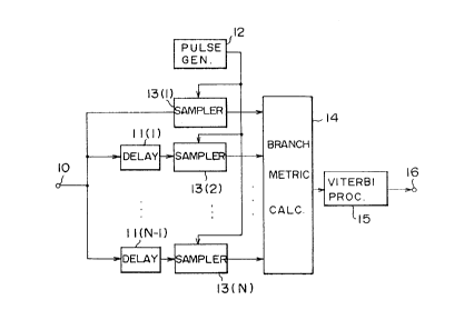
Referring to FIG. 1, represented by reference numerals
10, 11(1) through ll(N-1), 12, 13(1) through 13(N), 14, 15
and 16 are an input terminal, delay circuits to provide
different delay times, a pulse generator circuit, samplers,
a branch metric calculation circuit, a Viterbi processor
and an output terminal, respectively.
A received input signal through the input terminal 10
is delayed by a bank of delay circuits 11(1) through
ll(N-1) before reaching respective samplers 13(2) through
20S3749
13(N). Also, the received signal is directly applied to
the sampler 13(1) with no delay. The samplers 13(1)
through 13(N) perform signal sampling of the received
signal, and the outputs from the delay circuits 11(1)
through ll(N) at the timing of the pulse generated from the
pulse generator 12. When the sampling pulse frequency is
1/T, the delay times of the delay circuits 11(1) through
ll(N-1) are set to iT/N (i = 1, 2, ..., N-1), thereby
sampling the received signal in sequentially different
sampling phases by the samplers 13(1) through 13(N).
An alternative sampling means of sampling the received
signal in different sampling phases is illustrated in FIG.
10. Shown in FIG. 10 is a block diagram of one example of
the sampling means to perform sampling the received signal
in N different sampling phases using sampling pulses of N
(N > 1) different phases but each having a constant time
interval T. In FIG. 10, a reference numeral 1004 is an
input terminal, 1000 is a pulse generator to generate a
sampling pulse having frequency equal to 1/NT, 1001(1)
through lOOl(N) are frequency dividers to divide at
different phases, 1002(1) through 1002(N) are samplers and
100-3(1) through 1003(N) are output terminals.
In FIG. 10, the output from the pulse generator 1000
which generates the sampling pulse having the frequency
equal to 1/NT is frequency divided at different phase
angles by the frequency dividers 1001(1) through lOOl(N) to
supply the desired sampling pulses to the samplers 1003(1)
through 1003(N).
2083749
It is also possible to generate the sampling pulse
having the frequency equal to 1/LT (L < N) to generate the
signal sampled in N different phases by means of
interpolation and the like of the received signal sequence
sampled in L different phases.
The signals sampled by the samplers 13(1) through
13(N) are supplied to the branch metric calculation circuit
14 to obtain the branch metric. The branch metric circuit
14 may be constructed, for example, as shown in FIG. 5.
The outputs from the samplers 13(1) through 13(N) are
supplied to the input terminals 50(1) through 50(N). The
outputs to the input terminals 50(1) through 50(N) are
applied to both of the channel impulse response estimation
circuits 51(1) through 51(N) and the partial branch metric
calculation circuits 52(1) through 52(N).
Each of the channel impulse response estimation
circuits 51(1) through 51(N) may comprise a circuit to
obtain correlation between the received signal and the
preamble sequence as illustrated, for example, in FIG. 3 of
European patent laid-open number A2-0396101 (laid open on
November 7, 1990) when using the preamble sequence
exhibiting an impulse form of self-correlation function as
shown in Fig. 2, for example, in the above European patent
application. The channel impulse response estimation
circuits 51(1) through 51(N) output channel impulse
response vectors H(1) through H(N) of different sampling
phases from the signals sampled in different phases. Each
of the partial branch metric calculation circuits 52(1)
through 52(N) receive as inputs the channel impulse 2083749
response vectors H(1) through H(N) of different phases and
the signal sampled in the phase corresponding to the
sampling phase of the channel impulse response vector to
calculate the partial branch metric. The partial branch
metric will be obtained in the manner as given, for
example, in the right member of the equation in J. F.
Hayes, "The Viterbi Algorithm Applied to Digital Data
Transmission" IEEE, Communication Society, No. 13, p 18,
8b, 1975. The output from the partial branch metric
calculation circuits 52(1) through 52(N) are added to one
another in an adder 53 to output the branch metric from the
output terminal 54.
The calculated branch metric is applied to the Viterbi
processor 15 to derive the decision result
from the output terminal 16. The Viterbi processor 15 may
be realized by a normal soft decision Viterbi decoder
comprising an ACS (Add-Compare-Select) circuit and a path
memory (See, for example, Suzuki and Ta~ima,
"Implementation of Maximum Likelihood Decoder for
Convolutional Codes" Electronic Information Communication
Institute Report A, Vol. J73-A, No. 2, pp 225-231, February
1990).
This system can be easily applied to the diversity
reception system having a plurality of branches. That is,
each diversity branch is provided with a bank of delay
circuits 11(1) through ll(N-1), a pulse generator (12),
samplers 13(1) through 13(N) and a branch metric
2 ~ S ~
calculation circuit 14. The output from the branch metric
calculation circuit in each diversity branch is composed
by, for example, summation, thereby applying the composed
value to the Viterbi processor as the branch metric of the
entire diversity.
Illustrated in FIG. 2 is a block diagram of one
embodiment of the maximum likelihood sequence estimation
apparatus according to a second invention. In FIG. 2,
represented by a reference numeral 100 is an input
terminal, 101(1) through lOl(N) are pulse generators for
generating sampling pulses at the frequency (1/T) equal to
the symbol rate but in different phases, 102(1) through
102(N) are A-D (analog-to-digital) converters, 103(1)
through 103(N) are channel impulse response estimation
circuits, 104(1) through 104(N) are branch metric
calculator circuits, 105 is a branch metric composite
circuit, 106 is a Viterbi processor, and 107 is an output
terminal.
The input signal received at the input terminal 100 is
sampled and digitized by the A-D converters 102(1) through
102(N) at the timing of the respective pulses of different
phases generated from the pulse generators 101(1) through
lOl(N). The outputs from the A-D converters 102(1) through
102(N) are applied to the channel impulse response
estimation circuits 103(1) through 103(N) and the branch
metric calculation circuits 104(1) through 104(N).
Each of the channel impulse response estimation
circuits 103(1) through 103(N) may comprise a circuit to
2~ ~ 37 ~ ~
obtain correlation between the received signal and the
preamble sequence as illustrated, for example, in FIG. 3 of
European patent laid-open number A2-0396101 (laid open on
November 7, 1990) when using the preamble sequence exhibiting
an impulse form of self-correlation function as shown in Fig.
2, for example, in the above European patent application. The
channel impulse response estimation circuits 103(1) through
103(N) output channel impulse response vectors H(1) through
H(N) of different sampling phases from the signals sampled in
different phases. Each of the partial branch metric
calculation circuits 104(1) through 104(N) receive as inputs
the channel impulse response vectors H(1) through H(N) of
different phases and the signal sampled in the phase
corresponding to the sampling phase of the channel impulse
response vector to calculate the partial branch metric. The
partial branch metric will be obtained in the manner as given,
for example, in the right member of the equation in J. F.
Hayes, "The Viterbi Algorithm Applied to Digital Data
Transmission" IEEE, Communication Society, No. 13, p. 18, 8b,
1975.
The branch metric composite circuit 105 calculates
the branch metrics corresponding to the received signals of
different sampling phases obtained from the branch metric
calculation circuits 104(1) through 104(N), thereby outputting
the composite branch metric. The branch metric composite
circuit 105 may be configured, for example, as shown in FIG.
6. In FIG. 6, applied to the input terminals
' 74479-4
600(1) through 600(N) are the branch metrics co ~Qs8p~d~g
to the received signals of different sampling phases
derived from the branch metric calculation circuits 104(1)
through 104(N). The added output is derived from the
output terminal 602 as the composite branch metric. The
composite branch metric thus derived is applied to the
Viterbi processor 106 and the decision result
is derived from the output terminal 107.
The Viterbi processor 15 may be realized by a normal
soft decision Viterbi decoder comprising an ACS
(Add-Compare-Select) circuit and a path memory (See, for
example, Suzuki and Tajima, "Implementation of Maximum
Likelihood Decoder for Convolutional Codes" Electronic
Information Communication Institute Report A, Vol. J73-A,
No. 2, pp 225-231, February 1990).
Shown in FIG. 3 is a block diagram of one embodiment
of the maximum likelihood sequence estimation apparatus
according to a third invention. In FIG. 3, represented by
a reference numeral 200 is an input terminal, 201 is a
pulse generator circuit to generate a sampling pulse at
frequency (1/T) equal to the symbol rate, 202(1) through
202(N) are A-D converters, 203(0) through 203(N-1) are
delay circuits to provide respectively delay time iT/N (i =
1, 2, ..., N-1), 204(1) through 204(N) are channel impulse
response estimation circuits, 205(1) through 205(N) are
branch metric calculation circuits, 206 is a branch metric
composite circuit, 207 is a Viterbi processor, and 208 is
an output terminal.
2083749
The sampling pulse generated by the pulse generator
circuit 201 is directly applied to the A-D converter 202(1)
and also applied to the A-D converters 202(2) through
202(N) by way of the delay circuits 203(0) through
203(N-1). Sampling of the received signal supplied from
the input terminal 200 is performed in the A-D converters
202(1) through 202(N) whenever the sampling pulse is
applied thereto for digitizing the received signal. The
outputs from the A-D converters 202(1) through 202(N) are
supplied to the respective channel impulse response
estimation circuits 204(1) through 204(N) and branch metric
calculation circuits 205(1) through 205(N). Each of the
channel impulse response estimation circuits 204(1) through
204(N) receives as inputs the decision result
from the Viterbi processor 207 and the output from the
respective A-D converters 202(1) through 202(N) for
outputting the M dimensional channel impulse response
estimation vectors H(1) through H(N) corresponding to the
respective output from the A-D converter circuits 202(1)
through 202(N). Each of the channel impulse response
estimation circuits 204(1) through 204(N) may be
implemented, for example, as shown in FIG. 7.
In FIG. 7, applied to the input terminal 700 is the
decision result
from the Viterbi processor 207 while applied to the input
terminal 701 is the output from the respective A-D
converters 202(1) through 202(N). A replica of the
received signal is obtained by convolution of the decision
20~3749
result and the M dimensional channel impulse response
estimation vectors H(i), i = 1, 2, ..., N using an M-tapped
transversal filter 706. It is to be noted here that any
timing error between the replica of the received signal and
the actual received signal due to decoding delay time is
compensated by delaying the actual received signal from the
input terminal 701 using a delay circuit 703 (See, for
example, Proakis, "Digital Communications~, McGraw-Hill,
1983). A subtraction circuit 704 detects an error between the
output from the delay circuit 703 and the output from an adder
702. An adaptive control processor 705 sequentially updates
the channel impulse response estimation vector H(i) in such a
manner that the replica of the received signal is equal to the
actual received signal. An example of the adaptive control
processor 705 is an LSM algorithm (as described, for example,
in Proakis, "Digital Communications", McGraw-Hill, 1983) to
perform the following mathematical expression (1):
H(i)k+l = H(i)k + ,~(k)S(k) ~.- (1)
where, S(k) is the input to the delay circuit 708(1) and the
output signal vectors from the delay circuits 708(1) through
708(M+1) at time k or the vector comprising decision results
obtained from the time (k-(M-l))T to the time kT, ~(k) is an
error signal derived from the subtraction circuit 704 at time
k, and H(i) is the channel impulse response estimation vector.
In accordance with the above algorithm, H(i)k is updated to
output from the output terminals 707(1) through 707(M). Other
algorithms may be
74479-4
20~37~
applied as well.
Each of the branch metric calculation circuits 205(1)
through 205(N), the branch metric composite circuit 206 and
the Viterbi processor may be similar configuration to
104(1) through 104(N), 105 and 106 in FIG. 2, respectively.
Now, illustrated in FIG. 4 is a block diagram of an
embodiment of the maximum likelihood sequence estimation
apparatus in accordance with a fourth invention. In FIG.
4, represented by a reference numeral 300 is an input
terminal, 301 is a pulse generator to generate the sampling
pulse of the frequency (1/T) equal to the symbol rate,
302(1) through 302(N) are A-D converters, 303(0) through
303(N-1) are delay circuits to provide delay times it/N (i
= 1, 2, ..., N-1), 304(1) through 304(N) are channel
impulse response estimation circuits, 305(1) through 305(N)
are branch metric calculation circuits, 306 is a branch
metric composite circuit, 307 is a Viterbi processor, and
308 is an output terminal. The pulse generator circuit
301, the A-D converters 302(1) through 302(N), the delay
circuits 303(0) through 303(N-1), the branch metric
calculation circuits 305(1) through 305(N), and the Viterbi
processor 307 may be configured similarly to the pulse
generator circuit 201, the A-D converters 202(1) through
202(N), the delay circuits 203(0) through 203(N-1), the
branch metric calculation circuits 205(1) through 205(N),
and the Viterbi processor 207 in FIG. 3, respectively.
Each of the channel impulse response estimation circuits
304(1) through 304(N) may be configured as illustrated in
~ ~ ~ 3 7 4 9
FIG. 8.
In FIG. 8, represented by reference numerals 800 and
801 are input terminals, 802 is an adder, 803 is a delay
circuit, 804 is a subtraction circuit, 805 is an adaptive
control processor, 806 is an M-tapped transversal filter,
807(1) through 807 (M) and 810 are output terminals, 808(1)
through 808 (M-1) are delay circuits, and 809(1) through 809 (M)
are multiplier circuits. The difference between the channel
impulse response estimation circuits in FIGS. 7 and 8 is that
the output from the subtraction circuit 704 in FIG. 7 is
applied only to the adaptive control processor 705 while the
output from the subtraction circuit 804 in FIG. 8 is applied
not only to the adaptive control processor 805 but also to the
output terminal 810 as estimation process information. Also,
the branch metric composite circuit 306 receives as inputs the
branch metrics corresponding to the received signals of
different phases derived from the branch metric calculation
circuits 305(1) through 305(N) as well as the estimation
process information derived from the channel impulse response
estimation circuits 304(1) through 304(N) for outputting the
composite branch metric.
The branch metric composite circuit 306 may be
configured, for example, as illustrated in FIG. 9. In FIG. 9,
represented by reference numerals 900(1) through 900 (N) and
901(1) through 901 (N) are input terminals, 902(1) through
902(N) are power detection circuits, 903(1) through 903(N) are
comparator circuits, 904(1) through 904(N) are
~j 74479-4
2083749
gate circuits, 905 is an adder, and 906 is an output
terminal. In FIG. 9, applied to the input terminals 900(1)
through 900(N) are the signals on the output terminals
(810) from the channel impulse response estimation circuits
304(1) through 304(N) constituting the channel impulse
response estimation circuit in FIG. 8. Also, applied to
the input terminals 901(1) through 901(N) are the branch
metrics derived from the branch metric calculation circuits
305(1) through 305(N) corresponding to the channel impulse
response estimation circuits 304(1) through 304(N).
The power detection circuits 902(1) through 902(N)
detect the signal power from the respective input terminals
900(1) through 900(N) for application to the comparator
circuits 903(1) through 903(N). Each of the comparator
circuits 903(1) through 903(N) compares the input level
with a predetermined threshold level to output either "1"
or "0" if the input level is larger or smaller than the
threshold level, respectively. Such comparison output is
applied to the gate circuits 904(1) through 904(N). Each
of the gate circuits 904(1) through 904(N) disturbs the
signal from the input terminals 901(1) through 901(N) when
the input from the respective comparator circuits 903(1)
through 903(N) is "1", but allows the signal from the input
terminals 901(1) through 901(N) to pass when the input from
the comparator circuits 903(1) through 903(N) is "0". The
adder 905 adds only the branch metrics selected by the gate
circuits 904(1) through 904(N) to output the composite
branch metric from the output terminal 906. Hysteresis may
14
- be provided to the gate circuits 904(1) through 904( 2~ 8~ 7 ~ 9
that the signal is kept disturbed until the gate circuits
are reset if "1" is entered once. It is also possible to
apply to the input terminals 900(1) through 900(N) of the
branch metric composite circuit 306 the current channel
impulse response estimation vectors H(i)K (i = 1, 2, ....
N) for weighting the inputs from the input terminals 901(1)
through 901(N) in accordance with H(i)K (i = 1, 2, ..., N),
thereby obtaining the similar effect to the maximum ratio
composite diversity as described, for example, in S. Stain,
J. J. Jones, translated by Hideo Seki, "Modern
Communication Circuit Theory", Morikita Publishing Co.,
1970.
In case of applying the present invention to the burst
mode transmission such as TDMA and the like, it is also
possible to process the received signal after storing one
burst length of outputs from the samplers 13(1) through
13(N) in FIG. 1. The constructions as illustrated in FIGS.
2 through 4 are easily applicable to such system.
As apparent from the above description, the present
invention eliminates distortions due to sampling timing
error from the optimum sampling timing and inter symbol
interferences in a case of transmitting data by way of
channels causing inter symbol interferences.