Note: Descriptions are shown in the official language in which they were submitted.
- - 2~838 6 ~'
Docket No. UCL-lOlCIP
ELECTRONIC BALLAST AND PROTECTION CIRCUIT
BACKGROUND OF THE INVENTION
This invention relates to a compact, relatively low cost,
energy-saving electronic ballast that is particularly useful for
efficiently driving a fluorescent tube or a compact fluorescent
lamp. The ballast is characterized by a high power factor, low
total harmonic distortion and minimal radio frequency
interference and is adapted to be used with compatible tubes and
lamps from different manufacturing sources. A protection circuit
is connected to the ballast to prevent damage thereto in the
event that the tube or lamp is defective or disconnected from the
ballast or subjected to abnormal operating conditions.
Fluorescent tube and compact fluorescent lamp assemblies are
well known lighting devices. The fluorescent tube assembly
includes a tube and a separate electronic-ballast or adapter to
drive the tube. In the case of the compact fluorescent lamp
assembly, a lamp and ballast are combined as an integrated unit.
The conventional ballast that is associated with the
fluorescent tube assembly is typically heavy and large. Moreover,
such a ballast is not very energy efficient and is characterized
by a low power factor. The conventional ballast associated with
the compact fluorescent lamp assembly is also characterized by
a low power factor, unless size is sacrificed. Such a ballast
is also characterized by total harmonic distortion which, in many
cases, is not in full compliance with government regulations.
~Q8;~8~.
-
Because the compact lamp and electronic ballast are integrated,the entire lighting assembly must be discarded when the lamp is
damaged or reaches the end of its life. The foregoing results
in waste and inefficient use of materials, particularly in view
of the fact that the ballast is more costly to manufacture than
the lamp and commonly has a longer expected life span.
Ballasts are also known to fail because of certain failures
in the fluorescent tube or lamp. Consequently, the life of the
ballast is reduced and the frequency of replacement is increased,
whereby operating costs are correspondingly increased. Such
failures to the ballast may occur if power is applied when the
tube (i.e. load) is removed from the ballast or when an incorrect
or defective tube is connected to the ballast or the tube is
subjected to either a transient voltage surge or a high ambient
temperature that alters the electrical characteristics thereof.
It would therefore be desirable to overcome the
aforementioned shortcomings to fluorescent lighting devices by
providing a lightweight, compact, energy efficient electronic
ballast that would have low total harmonic distortion, minimum
radio frequency interference, and a high power factor (e.g. 0.9
or higher). Moreover, it would be desirable that the ballast be
detachable from the fluorescent lamp so that the lamp can be
replaced without the necessity of scrapping the ballast. In
addition, the ballast must comply with all government regulations
and be compatible with fluorescent tubes and lamps that are
produced by different manufacturers. Furthermore, it would be
desirable to have a protection circuit connected to the ballast
'~Qg3~1
to reduce failures thereof as a consequence of certain failures
in the tube or lamp.
SUMMARY OF THE INVENTION
In general terms, a circuit is disclosed for implementing
a relatively low cost, lightweight, energy efficient ballast for
driving a fluorescent tube or compact lamp. In accordance with
a first embodiment of the present invention, the ballast includes
a unique DC power supply comprising a high pass filter and a pair
of diode rectifiers, such that the input current is first
filtered and then twice rectified to provide the DC current
required to operate the ballast circuit. The ballast also
includes a high frequency oscillator and power output section
comprising the interconnection of a ferrite oscillator
transformer, first and second power transistors arranged in a
push-pull relationship, a ferrite choke coil, capacitors and
resistors. Also included is a section to trigger the oscillator
and thereby cause the fluorescent tube/lamp to ignite. The
trigger section will become inactive once the tube/lamp has
ignited.
In accordance with a second embodiment of the present
invention, a protection circuit is connected to the ballast to
avoid failure of the ballast due to certain failures to the
fluorescent tube or lamp. The protection circuit includes a
ferrite choke coil which is responsive to the output power of the
ballast, a transistor switch that operates to terminate the
ability of the ballast to oscillate and sustain damage during a
failure of the fluorescent tube, and a flip-flop circuit
;~$~3~1
connected between the choke coil and the transistor switch to
control the operation of said switch in response to the power
sensed by said coil. Under normal operating conditions, the
flip-flop is disabled, the switch is non-conductive and the
ballast oscillates in the usual fashion for driving the tube.
Under no load conditions, where the tube is damaged or
disconnected from the ballast, the flip-flop is enabled, the
switch becomes conductive and the oscillation of the ballast is
terminated.
BRIEF DESCRIPTION OF THE DRAWINGS
FIG. 1 shows a circuit having a unique DC power supply for
implementing the electronic ballast of the present invention for
efficiently driving a fluorescent tube or lamp;
FIG. 2a illustrates the input current waveform of the DC
power supply of a conventional electronic ballast;
FIG. 2b illustrates the input current waveform of the DC
power supply of the circuit of FIG. 1 after regulation;
FIG. 3a illustrates the output voltage waveform of the DC
power supply of a conventional electronic ballast;
FIG. 3b illustrates the output voltage waveform of the DC
power supply of the circuit of FIG. 1;
?,Sl.
FIG. 4a illustrates the output current waveform of the DC
power supply of a conventional electronic ballast;
FIG. 4b illustrates the output current waveform of the DC
power supply of the circuit of FIG. 1 after rectification; and
FIG. 5 shows a circuit having an electronic ballast, a
fluorescent tube to be driven by the ballast and a protection
circuit for enabling the ballast to survive certain failures of
the fluorescent tube.
DETAILED DESCRIPTION
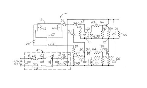
An electronic circuit 1 for implementing a relatively
compact, lightweight, low cost, and energy efficient ballast
which forms the present invention and which may be detachably
connected to a fluorescent tube 2 is initially described while
referring to FIG. 1 of the drawings. While a tube 2 is shown and
described, it is to be expressly understood that the ballast
circuit 1 may also be used with a compact fluorescent lamp. The
ballast circuit 1 includes a unique DC power supply 4 that is
connected to receive a 120 volt AC, 60 Hz input line signal. The
power supply 4 includes a pair of filter capacitors Cl and C2
that are connected in parallel with one another. Connected
between filter capacitors C1 and C2 are a pair of ferrite choke
coils LlA and LlB. Capacitors Cl and C2 and ferrite choke coils
LlA and LlB are interconnected to form a high pass filter 8.
Note the reverse connection of ferrite choke coil LlB relative
to coil LlA of filter 8 which contributes to producing a high
power factor. The high pass filter 8 will advantageously limit
the radio frequency interference produced by the AC input signal
so as to comply with government regulations regarding such
interference without consuming large amounts of power. Filter
8 is connected to a conventional diode bridge rectifier 6 by
which to provide half wave rectification of the filtered AC input
signal in the usual manner.
The DC power supply 4 includes a pair of rectification stage
output capacitors C3 and C5 that are connected in parallel with
one another and the diode bridge rectifier 6. A high speed
rectifier diode D2 is connected between output capacitors C3 and
C5. The capacitance of output capacitor C5 is preferably very
large relative to the capacitance of output capacitors C3 to
achieve a high power factor, as will soon be described. By way
of example only, the optimum values of the circuit components
which form the DC power supply 4 of ballast circuit 1 are given
as follows:
C1 = 0.1 to 0.22 ~F
C2 = 0.005 to 0.01 ~F
C3 = 0.005 to 0.01 ~F
C5 = 22 to 33 ~F
LlA = 0.01 to 0.015 Henries
LlB = 0.01 to 0.015 Henries
A first rectification stage output terminal 10 of power
supply 4 is formed at a common electrical junction with rectifier
6, diode D2, output capacitor C3, a current regulating capacitor
C4 and a resistor Rl. Current regulating capacitor C4 is
connected in series with the electrodes 12 and 14 of fluorescent
Sl
7-
tube 2 by way of a capacitor C7 which is connected between said
electrodes 12 and 14. Capacitor C7 may be either an integral
part of the fluorescent tube 2 (as shown) or part of the ballast
circuit 1. Electrode 14 is also connected in séries with a
ferrite choke coil L2 and a coil L3A which forms a ferrite
oscillator transformer 16. A second coil L3B of transformer 16
is connected to the base of a first power transistor TR1 via a
current limiting resistor R3.
A second rectification stage output terminal 11 of power
supply 4 is formed at a common electrical junction with rectifier
diode D2, output capacitor C5 and the collector of transistor
TR1. The diode bridge 6 and high speed diode D2 provide power
supply 4 with double rectification to provide the circuit 1 with
DC power necessary to obtain a high power factor. More
particularly, the first rectification stage output terminal 10
functions as a current summing junction, such that diode D2
rectifies the input current rectified by diode bridge 6 and
current from the tube 2 which passes through current regulating
capacitor C4. Accordingly, all of the DC current necessary for
operating the remainder of ballast circuit 1 is available from
the second rectification stage output terminal 11.
The emitter of transistor TR1 is connected to a common
electrical junction 18 with coils L3A and L3B of the ferrite
oscillator transformer 16 and a resistor R7 via a resistor R11.
Resistor R11 is connected in a feedback path with resistor R7
between the emitter and base of transistor TR1.
The collector of a second power transistor TR2 is also
connected to common electrical junction 18. The emitter of
3S~.
_ 8
transistor TR2 is connected to ground via a resistor 12.
Resistor R12 is connected in a feedback path with a resistor R6
between the emitter and base of transistor TR2. The base of
transistor TR2 is connected to a common electrical junction 20
by way of a current limiting resistor R4 and a diac D4. A coil
L3C which is magnetically coupled to the coils L3A and L3B to
provide reactance to the ferrite oscillator transformer 16, is
connected through a resistor R2 to a common electrical junction
24 formed with resistors R4 and R6 and the base of transistor
TR2.
With fluorescent tube 2 connected to ballast circuit 1, the
interconnection of power transistors TRl and TR2, ferrite choke
coil L2, ferrite transformer coils L3A, L3B and L3C, capacitors
C3 and C4 and rectifier diode D2 provides the ballast circuit 1
with high frequency oscillation and high power output for
efficiently driving fluorescent tube 2. When tube 2 is removed
from circuit 1, the aforementioned high frequency operation will
cease.
The aforementioned resistor Rl is connected in series with
a resistor R8 to form a voltage divider network. A resistor R9
is connected from the common electrical junction 20 with diac D4
to a point between voltage divider resistors Rl and R8. A
capacitor C6 is connected between common electrical junction 20
and ground. As will also be described in greater detail, the
interconnection of resistors Rl, R4 and R9, diac D4 and capacitor
C6 provides the ballast circuit 1 with a trigger capability.
A diode D5 is connected across the interconnection of
resistor Rll with the emitter and collector of transistor TRl,
~r ~
. 9
and a resistor R5 is connected across the diode D5. Another
diode D6 is connected from common electrical junction 18 to
ground. Thus, diode D6 is connected across the interconnection
of resistor R12 with the emitter and collector of transistor TR2.
Diodes D5 and D6 are included to protect power transistors TRl
and TR2 against voltage surges. A diode D3 is connected from the
common electrical junction 20 with diac D4, resistor R9 and
capacitor C6 to the coil L3A of transformer 16 by way of a
resistor R10. Diode D3 and resistor R10 are included to disable
the aforementioned trigger after ballast circuit 1 begins its
high frequency oscillation.
The operation of the ballast circuit 1 of FIG. 1 is now
described. The 60 Hz source or line voltage signal initially
passes through the high pass filter 8 of DC power supply 4. The
line voltage signal is then rectified at the diode bridge
rectifier 6. The half wave rectified 120 Hz signal is regulated
by a high frequency current (in the order of tens of kHz) through
current regulating capacitor C4 (best illustrated by the waveform
of FIG. 4b). The majority of the high frequency current from
capacitor C4 flows through the first rectification stage output
terminal 10 of power supply 4 to output capacitor C5 by way of
diode D2 at which said current is rectified. However, a minor
portion of the high frequency current through capacitor C4 flows
to output capacitor C3 via output terminal 10. Being that the
inductance of high pass filter 8 is relatively low, as indicated
above, little reactance is provided for the 60 Hz line voltage,
but a high resistance is provided to the high frequency current
added to the 120 Hz current at output terminal 10 (see FIG. 4b).
- 10
With regard to the trigger operation of ballast circuit 1,
positive current flowing through resistors R1 and R9 will be
applied to capacitor C6. When the voltage across capacitor C6
increases to about 30 to 32 volts, the diac D4 will produce a
pulsating current flowing through resistor R4 to the base of
power transistor TR2 to trigger the oscillator of ballast
circuit 1. When the voltage across capacitor C6 drops to about
3 volts, the trigger is disabled.
The current flowing in coil L3A of ferrite oscillator
transformer 16 is magnetically coupled to coils L3B and L3C.
Thus, with power transistors TR1 and TR2 working in standard
push-pull fashion, an oscillator is created which operates in the
40-70 kHz range (depending upon the particular fluorescent tube
2 being used). Being that an oscillator is common to
conventional ballast circuits, a detailed description of the
operation of the oscillator of ballast circuit 1 will not be
described.
Ferrite choke coil L2, which is connected in series with
electrode 14 and coil L3A of transformer 16, provides two
important functions. Prior to ionization and the ignition of the
fluorescent tube 2, ferrite choke coil L2 cooperates with
capacitor C7 to provide the high voltage necessary between
electrodes 12 and 14 to ionize the gas in tube 2. What is more,
after the tube 2 is ignited, ferrite choke coil L2 limits the
current, whereby to stabilize the operation of tube 2.
;2r~ 5~;3~il
Considering now the formula RL = 2~fL, where:
R~ = the reactance (equivalent resistance) of L
f = frequency
L = inductance.
When 2L is known, RL is directly proportional to f. That is to
say, when the frequency increases, reactance also increases,
thereby resulting in corresponding changes to the waveform of the
input current.
The foregoing is best illustrated while referring to FIGs.
2-4 of the drawings. FIGs. 2a, 3a and 4a show waveforms
associated with the DC power supply of a typical electronic
ballast, while FIGs. 2b, 3b and 4b show corresponding waveforms
associated with the power supply 4 of ballast circuit 1 of FIG.
1. In practice, the time to charge the output capacitor of the
power supply of a conventional ballast circuit is very short.
Therefore, the waveform of the input current will be pulsating
(best illustrated in FIG. 2a). Hence, the RMS current is large,
the power factor is only about 0.5, and the harmonic content will
typically exceed 90%. In the DC power supply 4 of ballast
circuit 1, the 120 Hz half waveform current at output capacitor
C3 and the 40 to 70 kHz current produced by the oscillator of
ballast circuit 1 regulate each other. Moreover, the high pass
filter 8 and diode D2 cause the current applied to output
capacitor C5 via second rectification stage output terminal 11
to be very smooth and even (best illustrated in FIG. 4b). Thus,
and is best shown by comparing FIGs. 2a and 2b, the RMS of the
AC input current is reduced by about 39% or more in the DC power
supply 4 of FIG. 1 relative to the RMS of the AC input current
3~
-
- 12
to the power supply of the conventional ballast. Changing the
pulsating input current waveform shown in FIG. 2a to the near
sinusoidal input current waveform of FIG. 2b greatly reduces the
input current harmonics and advantageously raisés the power
factor from 0.5 to about 0.9, or more.
The following list represents the optimum parameters of
other components of ballast circuit 1:
C4 = 0.01-0.1 ~F
C6 = 0.04-0.068 ~F
Rl = 470k Ohm
R2 = R3 = 12-18 Ohm
R4 = 15 Ohm
R5 = 220k Ohm
R6 = R7 = 68 Ohm
R8 = R9 = 33Ok Ohm
R10 = 10k Ohm
R11 = R12 = 0-2.7 Ohm
TRl = TR2 = Part No. LSE1305 or equivalent
D2 = D3 = D5 = D6 = Part No. FR104 or equivalent
D4 = Part No. HT-32 or equivalent
The ballast circuit 1 may be detached from the fluorescent
tube 2 at suitable plug-in connection terminals 24. Thus,
ballast circuit 1 may be reused with a new tube in the event that
an old tube is detached therefrom and discarded. The circuit 1
is advantageously of compact design and lightweight and,
therefore, adapted to be used in conventional fluorescent
lighting assemblies with the tubes or compact lamps which are
available from different manufacturers and have a variety of
_ 13
configurations, such as conical, oval, rectangular or
cylindrical.
FIG. 5 of the drawings illustrates a protection circuit 30
that is electrically connected to an electronic baliast lA which
drives a fluorescent tube 2. The protection circuit 30 is
particularly useful for enabling the ballast lA to survive
certain failures of the fluorescent tube 2 as well as abnormal
operating conditions, whereby to increase the operating life of
the ballast and correspondingly reduce operating cost by avoiding
frequent ballast replacement. Since the circuit for the
electronic ballast lA of FIG. 5 is substantially the same as the
circuit for the electronic ballast 1 previously described when
referring to FIG. 1, the circuit of ballast lA will not be
described in detail, although like reference numerals have been
used to represent identical electrical components.
However, with regard to ballast lA, it is pointed out that
resistors R8 and R9 of ballast 1 have been deleted, and resistor
Rl is connected directly to the common electrical junction 20
with diac D4, capacitor C6 and diode D3. Therefore, a circuit
path is established between the DC power supply 4, at terminal
10, and the soon to be described protection circuit 30. More
particularly, resistor Rl is connected to rectification stage
output terminal 10 (or 11) to develop a DC voltage to be supplied
to electrical junction 20 to operate capacitor C6 and diode D4.
The protection circuit 30 which is connected to ballast
circuit lA includes three transistors TR3, TR4 and TR5. The
collector of transistor TR3 is connected to ballast lA at the
common electrical junction 24 with the base of transistor TR2 and
- 21)~38~
14
resistors R2, R4 and R6. The emitter of transistor TR3 is
connected to the common electrical ground. Thus, the conduction
path of transistor TR3 is connected to the aforementioned circuit
path from fluorescent tube 2 including capacitor C4, diac D4 and
resistors R1 and R4. The base of transistor TR3 is connected at
a common electrical junction 32 with one plate of a capacitor
C10, each of series connected resistors R17 and Rl8, and the
emitter of transistor TR4.
The collector of transistor TR4 is connected at a common
electrical junction 34 with a resistor R16, one plate of a
capacitor C8, and the base of transistor TR5. The base of
transistor TR4 is connected at a common electrical junction 36
with resistors Rl3 and Rl7, the second plate of capacitor ClO and
the collector of transistor TR5. The emitter of transistor TR5
is connected at a common electrical junction 38 with the second
plate of capacitor C8. The protection circuit 30 is connected
from common electrical junction 38, via a resistor R14, to the
output terminal 11 of the DC power supply of ballast lA which was
disclosed when referring to FIG. 1.
Thus, a circuit path is established in protection circuit
30 from electrical junction 38 to electrical ground via the
conduction path of transistor TR5 and the series connected
resistors R17 and R18. A capacitor C9 is connected across the
aforementioned circuit path from electrical junction 38 to
ground, and a resistor R15 is connected in parallel with
capacitor C9.
Protection circuit 30 also includes a ferrite choke coil L2B
which is magnetically coupled to the ferrite choke coil L2A of
_ 15
ballast lA to work together in a fashion similar to a magnetic
transformer. The aforementioned resistor R13 is connected from
the common electrical junction 36 to electrical ground via a
diode D7 and the choke coil L2B.
The operation of the protection circuit 30 in combination
with a replaceable fluorescent tube 2 and the ballast circuit lA
is now disclosed. The circuit 30 is adapted to provide
protection to ballast lA under the following operating
conditions: (1) the fluorescent tube is removed from ballast lA
(i.e. eliminating the load); (2) the tube is damaged, the
incorrect tube is connected, or the tube is subjected to a
transient voltage surge; and (3) the tube is subjected to a high
ambient temperature effecting the electrical characteristics
thereof. Some of the aforementioned conditions would occur if
the respective filament electrodes 12 and 14 of the tube 2 are
shorted, the tube has no filament electrode, or the tube receives
no filament current, such as where both the electrodes 12 and 14
function as anodes.
As important features of the present invention, transistors
TR4 and TR5 are coupled to one another in the manner previously
described such that said transistors TR4 and TR5 and resistors
R16, R17 and R18 form a flip-flop circuit 40. The output power
of the ballast lA is sensed by ferrite coil L2B, diode D7,
resistor R13 and capacitor C10. Transistor TR3 is selected to
have a low saturation voltage and functions as an ON/OFF switch
to control the oscillation and power output of the ballast lA,
depending upon the condition of the tube 2 to be driven thereby.
16
Under normal operating conditions, when a suitable
fluorescent tube 2 is connected to ballast lA, said tube is the
load of the ballast. At this time, and depending upon the
characteristics of tube 2, the voltage of capacitor C7, which is
connected in series with electrodes 12 and 14, is about 35 to 80
volts, and the current through series connected ferrite choke
coil L2A is about 200-350 milliamps whereby to ignite the tube
2. Due to its inductive coupling to coil L2A, a corresponding
current is induced in the ferrite choke coil L2B of protection
circuit 30, which current is half wave rectified by diode D7.
This half wave rectified current passes through resistor R13 and
capacitor C10 which smoothes the waveform and produces a
potential of about 0.15 to 0.30 volts DC between common
electrical junction 36 and electrical ground. The voltage at
electrical junction 36 (i.e. at the base of transistor TR4) is
insufficient to trigger transistor TR4, whereby the flip-flop 40
comprising transistors TR4 and TR5 is disabled and the protection
circuit 30 rendered ineffective.
In the case where the fluorescent tube 2 is either damaged
or disconnected from ballast lA, the effective load of the
ballast is removed. Therefore, the voltage between electrodes
12 and 14 will be increased to a few hundred volts. Moreover,
current which may be as high as 500 to 1500 milliamps (depending
upon the configuration of coil L2A) passes through capacitor C7
and coil L2A without igniting the tube. Due to its coupling to
coil L2A, a corresponding current is induced in ferrite choke
coil L2B which passes through diode D7, resistor R13 and
capacitor C10. Thus, the voltage at common electrical junction
~ 17 ~r ~5'~
36 is increased so as to trigger transistor TR4 and thereby
enable the flip-flop 40. Accordingly, DC current flows through
resistors R14 and R16, the collector/emitter conduction path of
transistor TR4, to the base of trigger transistor TR3, whereby
transistor TR3 is rendered conductive. Because of the low
saturation voltage requirement of transistor TR3, when said
transistor TR3 is conductive, the peak voltage between common
electrical junction 24 (at the base of transistor TR2 of ballast
lA) and electrical ground will be held below 0.4 volts which will
cause transistor TR2 to become disabled. Thus, the trigger
transistor TR3 functions as a protection switch to selectively
disable ballast lA. That is to say, the push-pull operation of
ballast transistors TR1 and TR2 ceases, the ability of ballast
lA to oscillate is thereby terminated and the ballast lA is
advantageously protected against damage and the need for
replacement.
In the case where either the wrong fluorescent tube is
connected to ballast lA, or the ballast is subjected to a voltage
surge from the power supply, or an ambient temperature increase
changes the operating characteristics of the tube, the current
passing through magnetically coupled coils L2A and L2B increases
and, in the manner described immediately above, the flip-flop 40
is enabled, trigger transistor TR3 is rendered conductive, the
push-pull operation of transistors TRl and TR2 ceases, and the
ballast lA is advantageously protected.
After the problem which caused the protection circuit 30 to
be activated has been resolved or a new fluorescent tube has been
suitably connected to ballast lA, choke coils L2A and L2B have
18
no current, the flip-flop 40 is disabled, trigger transistor TR3
becomes non-conductive, and the protection circuit is switched
off. The protection circuit 30 will be reset in about 10-25
seconds after the AC input power has been manually switched off
and then on. The ballast lA and tube 2 will then begin to
operate normally, such that protection circuit 30 once again
becomes ineffective until a new abnormality is detected.
By way of example only, the optimum values of the circuit
components which form the protection circuit 30 are given as
follows:
R13 = R14 = 120k-240k ohm
R15 = 20k-39k ohm
R17 = 20k-68k ohm
TR3 = TR4 = NPN transistor
TR5 = PNP transistor
D7 = switching diode
C8 = C9 = 0.047 ~F-0.22 ~F
C10 = 22 ~F-100 ~F
L2A = 0.001-0.006 Henries
L2B = 2-5 turns
It may be appreciated that where the fluorescent tube 2
develops a short circuit between electrodes 12 and 14, no current
will flow. However, because of current regulating capacitor C7
connected in series with electrodes 12 and 14 and ferrite choke
coil L2A connected to an output terminal of the ballast lA at
electrode 24, a high voltage (e.g. as high as 1000 volts) will
be created to thereby ionize the gas within the tube 2, allow
current to flow and light to be generated. Accordingly, the
~838 ~ ~
19
temperature inside the tube is heated and consequently, the
resistance is reduced. Once this resistance is sufficiently
reduced, the tube operating voltage will also be reducéd to
normal. Unlike conventional ballasts, the foregoing enables the
ballast lA to start tube 2 when the filament electrodes are
shorted or missing.
It will be apparent that while a preferred embodiment of the
invention has been shown and described, various modifications and
changes may be made without departing from the true spirit and
scope of the invention.