Note: Descriptions are shown in the official language in which they were submitted.
2 ~ 6 5
T~-9499
SUBSTRATE FOR OPTICPI, RECORDING ~EDIUM AND
MAGNETO-OPTIChL RECORDING MEDIUM USING SAME
sAcKGRouNn OF THE INVENTION
1. Field of the Invention
The present invention relates to a substrate
for an optical recording medium, particularly suitable
for a magneto-optical recording medium capable of direct
overwrite ~y modification of power level and/or pulse
width of the recording optical pulse, and also relates to
such a magneto-optical recording medium using said
substrate.
2. Description of the ~elated Art
Optical dlscs have been intensively
investigated, developed and commercialized as high
density and capacity information storage media. The
commercialized optical discs have, adjacent to data
areas, a guide in the form of a convex or concave portion
on the surface of the substrate for servo tracking by an
optical beam during recording, reproduction, erasing,
etc., of information~ The typical guide is a groove
formed on the surface of the substrate in the form of
spiral or concentric circles. The control of the
tracking servo is conducted by a light reflected from the
guide.
It is however known that the quality of signal
is degraded by the guides existing in the vicinity of the
data areas. The convex or concave guides re~1ect -to the
recording layer which causes a deformation of bit
configuration lowering ~he C/N ratio (carrier to noise
ratio), etc.
Some solutions have been proposed to solve the
above problem. For example, U.S. Patent No. 5,089,358,
issued on February 18, 1992 for Taki et al, discloses a
flat layer formed on a base plate to provide a flat
surface on which a recording layer is formed so that the
2~3~
signal reproduced from the'recording layer is not
deteriorated. Taki et al form the guides by patterning a
metal reflecting layer deposited on a glass base plate,
followed by making the flat layer on the guides. This
process re~uires complex steps such as photoli-thography
and etching and is not adequate for mass production due
to low yield and high cost, etc.
JP-A-57-6054~, published on April 12, 1992,
discloses a planalizing resin layer formed on a resin
substrate having convex or concave portions, as a
tracking servo guide on the surface thereof. In
JP-A-57-60544, since both the planali~ing layer and the
substrate are made of a resin, the light reflection from
the tracking servo guide is disadvantageously low due to
a small difference of the refractive index thereof so
that the tracking servo is not efficient.
JP-~-2-152041, published on June 12, 1990,
discloses a planalizing layer of silicon nitride on a
substrate by sputtering or evaporating silicon nitride
' 20 onto a substrate while milling the surface of the
deposited silicon nitride layer. This sputtering or
evaporation while milling is complex and does not provide
~ a planalizing layer having a desired planer top surface.
; - JP-B2-4-47910, published on August 5, 1992,
discloses a thin film coating on a substrate having
'~ convex or concave portions as tracking servo guides, in
which the thin film coating covers the sharp angle edges
of the convex or concave portions and provides a
relatively flat or smooth top surface by which a
recording layer to be formed thereon would not be
damaged. In JP-B2-4-47910, if the thin film coating is
an organic resin layer, a sufficient difference in the
refractive index between the thin film coating and the
substrate cannot be obtained, and if the thin film
coating is an inorganic layer, the top surface of the
thin film coating cannot be made geometrically planar,
causing the S/N ratio to be lowered due to still existing
~3~
-- 3
geometrical convex or concave portions.
The object of the instant invention is to solve
the above problems, to provide a substrate fox an optical
r~cording medium by which a reliably high tracking signal
is obtained irom the guides for a tracking servo and an
enhanced ~uality of reproduced signal can be obtained due
to a recording layer being formed on a geometrically
planar surface of the substrate, and which can be
produced at a high yield and a low cost, and to provide a
magneto-optical recording medium using such a substrate.
SUMMARY OF THE INVENTION
To attain the above and other ob~ects of the
invention, the presen-t invention provides a substrate for
an optical recording medium, comprising a base having
guide means in the form of convex or concave portions for
servo tracking with an optical beam, the base being made
of an organic resin material in at least a portion
thereof where the guide means is formed; a dielectric
layer on the base at least in an area where the guide
means is formed; and a planalizing layer on the
dielectric layer and the base for burying the convex or
concave portion of the guide means and making a top
surface of the planalizing layer flat; wherein the
dielectric layer has a refractive index higher than those
of the organic resin material forming the guide means and
the planalizing layer.
The present invention also provides a magneto-
optical recording medium comprising A) the substrate as
described above and B) a magneto-optical recording layer
over the substrate, the magneto-optical recording layer
being capable of being directly overwritten by
modification of a power level and/or pulse duration when
recording an optical pulse.
BRIEF DESCRIPTION OF THE lNV~N'l'lON
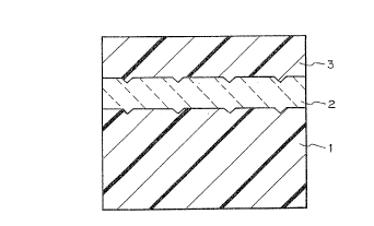
Figure 1 schematically illustrates a substrate for
an optical disc of the present invention.
Fig. 2 shows the dependency of the reflectivity on
- 4 _ ~83~6~
the AlSiN layer thickness 2 in the structure as showql in
Fig. 1.
Figs. 3A and 3B show the pulses used to write and
overwrite in an embodiment of the present invention.
Fig. 4 is a cross-sectional view of a magneto-
optical recording medium of Example 1.
Figs. 5 and 6 are cross sectional views of magneto-
optical recording media of Comparative Examples 1 and 2,
respectively.
Fig. 7 is a cross-sectional view of a magneto-
optical recording medium of Example 2.
Figs. ~ and 9 are cross-sectional views of magneto-
optical recording media of Comparative Examples 3 and 4.
Figs. 10 and 11 are cross-sectional views of
magneto-optical recording media of Examples 3 and 4.
DETAILED DESCRIPTION OF THE INVENTION
In the present invention, a light reflected from
guides for servo tracking is utilized to control the
tracking servo. It is necessary to obtain a sufficient
intensity of the reflected light from the guides to
attain a stable tracking servo capability. Specifically,
at least 10% of the reflection of a tracking servo light
beam from the guides is preferred. To attain this
condition, it is sufficient that a dielectric layer of a
material having a refractive index higher than that of
the base forming the guides and that of the planali~ing
layer and having a high transparency is disposed at least
on the guides. Since the typical resin materials of the
base including the guicle portions has a refractive index
of 1.4 to 1.6, it is preferred that the dielectric layer
has a refractive index of not less than 1.6 for the
wavelength of the light beam for servo tracking, to
obtain a sufficient intensity of reflected light.
Materials satisfying the abo~e conditions include
AlN, ZnS, Si3N4, ~lSiN, SiO, Zr2O3, In2O3, SnO2, TazO5,
AlON, SiON, ZrON, InON, SnON and TaON, and mixtures
thereof.
~3~6~
-- 5 --
The percent reflection of light for servo tracking
i6 more preEerably not less than 15% to obtain a stabler
servo tracking capability and a higher reproduction
signal intensity. To attain this, the refractive index
of the dielectric material is preferably not less
than 1.3 for the wavelength of light for servo tracking.
In this respect, inorganic oxides and/or nitrides such as
AlSiN, Si3N4, Zr2O3, Ta2O5, ~rON and TaOM are preferable
and from the viewpoint of durability AlSiN is
particularly preferable.
When n layexs are stacked, a layer Im having a
refractive index of nm and a thickness of hm is
sandwiched by a layer Im1 having a refractive index of
nm1 and a layer Im+1 having a refractive index of nm+1, and
a light having a wavelength of A is incident from the
layer ~m+1 side, the amplitude reflection ~,m+1 is
expressed by the following formula:
rm1m + rmm+1 exp (~2j~m)
~.m+1
l + rm1,m rm,m+l exp (-2j~)
n" l - nm
25 where rm-1,m = ~ ~ ... (2)
nm l ~~ nm
2~ n~ h~
~m = -~ (3)
A
and j denotes the complex number.
The total reflection can be obtained by adding all of the
reflections from the interfaces between adjacent layers.
For example, in the three-layer construction as
shown in Fig. 1, when the base 1 is polycarbonate, having
a refractive index of 1.58, the dielectric layer 2 is
AlSiN having a refracti~e index of 2.05, the planalizing
layer 3 is a resin having a refractive index of 1.50, and
- 6 - 20838~S
the thickness of the dielectric layer is varied, the
total reflection from the three-layer construction is
shown in Fig. 2.
A higher reflection is periodically obtained when
the thickness o-f the dielectric layer is varied. Any
thickness of -the dielectric layer providing a higher
reflection may be advantageously used, but a thin
thickness is preferable from the viewpoint of
productivity.
Such a preferable thickness of the dielectric layer
depends on the refractive index of the dielectric layer.
When the dielectric layer is an inorganic nitride, oxide
or the like, the refrac-tive index thereof is in a range
of 1.6 to 2.3 and the thickness of the dielectric layer
is preferably in a range o~ 20 nm to 160 nm.
When the degree of the nitrization and/or oxidation
of the nitride and/or oxide dielectric layer is lowered,
the recording and reproduction characteristics are
affected but the refractive index is increased so that
the thickness of the dielectric layer can be made thinner
and the productivity is improved.
The dielectric layer may be a single layer or a
multi-layer of different materials.
The dielectric layer can be formed by any process
including PVD such as evaporation, sputtering and CVD or
the like. It is preferred for optical discs that the
dielectric layer is firmly adhered to the substrate to
prevent peeling of the dielectric layer during high
temperature and high humidity durability tests and the
sputtering process is preferred in this respect.
The dielectric layer is formed on at least the
guides but is preferably formed on the entire surface of
the base including the guides since it is easy to make.
When such a dielectric layer having a thickness of
around 100 nm is deposited on the guides or base, the top
surface of the dielectric layer retains the configuration
of the guides and cannot be geometrically planar. Since
2~3~5
-- 7
the light re-flection depends on the thickness of the
dielectric layer, the thickness of the dielectric layer
is generally selected so that the light reflection from
the data areas, i.e., areas without guides of convex or
concave portions, becomes maximum. It is preferred that
the dielectric layer has a uniform thickness along the
top surface of the base including the guide portions so
that the light re~lection from the guides is also almost
maximum. It is preferred that the difference of the
thickness of the dielectric layer along the layer is less
than 10%.
In the instant invention, the convex or concave
portions of the top surface of the dielectric layer due
to the guides are buried, for example, by coating a
material having a low viscosity to make the top surface
geometrically planar on which a recording layer is to be
formed so that the configuration of the recording bits is
not affected due to the presence of -the guides and a high
quality reproduction signal can be obtained due to
~0 perfect bit configuration. The difference of the level
of the top surface of the planalizing layer is preferably
less than a few tens nanome-ters.
The thickness of the planalizing layer is preferably
in a range of 50 nm to 500 nm on the guides. Since the
guides have a depth or height of more than 40 nm, the
planalizing layer should preferably have a thickness of
50 nm or more to bury the guides. The thickness of the
planalizing layer is preferably 500 nm or less when
productivity is considered.
rrhe material to be used for the planalizing layer is
not particularly limited as long as i-t can bury the
convex or concave portions of the guides and provide a
planar top surface, but is preferably a resin due to easy
formation of -the layer.
Such resins include any resins which can be used for
optical discs, for example, ultra-violet ray curable
resins, electron beam curable resins, epoxy resins,
3 ~ ~ ~
silicate resins, urethane resins, polyester resins,
thermoplastic resins, etc.
~ It is preferred, however, that the resins can be
solved in general organic solvents since the resins are
to be coated at a lowered viscosity prepared by diluting
with a solvent.
In the production of optical discs, W-curable
resins and electron beam curable resins are often used
because of their high productivity and excellent
protection effect or the like. The W-curable resins are
most often used because equipment therefor is simpler
than that of the electron beam curable resin. Such W-
curable resins are commercially available as compositions
comprising a compound called acrylate of oligomer, having
a relatively high molecular weight and obtained by
acrylating or metacrylating a compound or oligomer having
a functional group such as hydroxyl or epoxy, for
example, acrylate of a bisphenol A--based epoxy compound
or oligomer, a compound having one functional group,
e.g., (meth)acryloyloxy, or two to six functional groups,
e.g., (meth)acryloyloxy, and an initiator. For example,
SD-17, SD-301, etc., produced by Dainippon Ink and
Chemicals, Inc. and UR-4502 produced by Mitsubishi Rayon
are commercially available. Also, MH-71 produced by
Mitsubishi Rayon, for example, is commercially available
as an electron beam curable resin.
; Epoxy resins can be any ones that can be used for
optical discs, typically ones derived from bisphenol.
Nevertheless, since transparency is required for optical
discs, the curing agent should be carefully selected.
From the viewpoints of curing rate and transparency,
pentaerythritol-derived diamine and the like are
preierably used and, for example, Epomate N-002 produced
by Yuka Shell Epoxy can be mentioned as a preferred
curing agent.
Silicate resins are also any ones that can be used
for optLcal discs, including thermoplastic types such as
2~83~6~
alkylsilo~ane, and W -curable types such as acryl
silicone compound. For e~ample, glass resin GR-650
produced by Showa Denko and KP-f5 and KNS 5300 produced
by Shin-Etsu Chemical Co. Ltd. can be used.
Thermoplastic resins that can be used are those
which do not affect the recording layer, are soluble in
an adequate solvent, particularly an organic solvent and
provide a uniform transparent layer. For example,
acrylates resin such as polymethylmethacrylate and
polyethylmethacrylate, acrylonitrile resins such as
~ polyacrylonitrile and polymethacrylonitrile, fluorine-
; based resins such as vinyl fluoride-hexafluoropropylene
copolymer, vinyl resins such as vinyl chloride and vinyl
acetate, polyvinyl~alcohol resins, polyvinylbutylal
resins, polyester resins, polyurethane resins, etc., and
mixtures and copolymers thereof can be preferably used.
The planalizing layer can be formed by spin coating,
screen printing, roll coating t spray coating, dipping,
sputtering, etc. When the planalizing layer is a cured
resin layer, the resin layer is preferably applied by
coating a resin or a diluted resin solution from the
viewpoint of workability. Further, spin coating is the
most preferable considering the productivity, cost, etc.
When the planalizing layer is applied by a spin
coating method, the viscosity o~ the resin to be applied
must be low, e.g., by diluting a resin material with a
solvent. Preferred viscosity of the resin solution to be
applied by spin coating is not more than 50 cP at 20~C to
obtain a layer thickness of 200 to 500 nm and not more
30 than 30 cP at 20~C for a layer thickness of 50 nm to
200 nm.
The solvent for dilution may be any ones that for an
organic resin base do not cause chemical damage to the
base and can be almost volatilized during the curing of
the resin. Preferred solvents include isopropylalcohol,
butylalcohol, ethylalcohol, etc., from the viewpoint of
handling poisonous materials.
lo 2~3~5
The guides formed on the top surface of the base are
typically grooves, but are not limited thereto. The
grooves preferably have a depth of not less than 40 nm to
; obtain a stable servo tracking capability and more
preferably not less than 70 nm to obtain a more stable
servo tracking capability. The configuration of the
grooves as the guides is not particularly limited but a
V-groove is preferred to make the reflections from the
guides and the dielectric layer overlying the guides
e~ficient.
The material of the base is preferably an organic
resin at least at a portion where the guides are formed.
Both of a base entirely made of a single organic resin
and a base with a cured resin layer prepared by the
2P(photo polymer) method to provide guides on the surface
of the base can be used as the base of the present
invention.
The organic resins used for the base include
polycarbonate resins, acryl resins, epoxy resins, 2-
methyl pentene resin, polyolefin resins, or copolymersthereof. A~ong others, polycarbonate resins are
preferred from the viewpoints of mechanical strength,
durability, thermal resistance, transparency and cost.
It is preferred to prepare the entire base by a
polycarbonate resin from the viewpoint of productivity.
The guides used at the present for servo tracking
are V-grooves in the form of a concentric circle or
spiral at a pitch of about 1.6 ~m with a groove width of
about 0.6 ~m and a group depth of typically 70 nm.
Nevertheless, the configuration of the guides and track
pitch are not limited to the above in the present
invention.
The recording layer to be formed on the substrate
prepared as described above is not particularly limited.
Magneto-optical recording layers of amorphous rare earth
element-transition metal alloys, inorganic or organic
phase-transition type recording layers, write once-
2~3~6~
11
. .
recording type recording layers, or any other optical
recording layers can be used.
Specifically, the optical recording layer can be
sandwiched by transparent dielectric layers, a reflecting
metal layer can be inserted on a side of the recording
layer opposite to the light incident side, and/or an
inorganic and/or organic protecting layer can be provided
over the recording layer.
Further, although a magneto-optical recording la~er
is sandwiched by transparent dielectric layers to enhance
the Kerr effect and the thus sandwiched structure is to
be formed on the planalizing layer of the substrate, the
dielectric layer between the recording layer and the
planalizing layer may be eliminated by utilizing the
planalizing layer as the enhancement layer. In this
case, the thickness of the planalizing layer is
preferably 200 nm to 300 nm to obtain a maximum
enhancement effect. The material of the planalizing
layer is not particularly limited and may be, for
example, W -curable resin, electron beam curable resin,
epoxy resin, silicate resin, urethane resin, polyester
resin, thermoplastic resins, or the like.
The substrate for an optical recording medium of the
present invention is particularly advantageously
applicable to a magneto-optical recording medium which
can be overwritten only by modification of power level
and/or pulse width of an optical pulse.
The drawback of the magneto-optical recording media
in comparison with floppy discs, hard discs, etc., is the
fact that direct ove~rite is difficult. Here, the
direct overwrite means writing information while erasing
already written information.
Various direct overwrite methods have been proposed
for magneto-optical recording media. Among others, a
me~hod disclosed in ~.S. Patent No. 4,888,750;
J. Appl. Phys. Vol. 63 No. 8 (1988) 3844; IEEE TR~NS.
- 12 - 2 0~ 8~
Magn. Vol. 23 No. 1 (1987) 171; Appl. Phys. Lett~ Vol. 49
No. 8 (1986) 473; IEEE TRANS. Magn. Vol. 25 No. 5 (1989)
3530; J. Appl. Phys. Vol. 69 No. 8 (1991) 4967; and
others has attracted attention because it does not
require modification of the conventional magneto-optical
i recording apparatus in their optical system, magneto and
so on. The proposed method uses a magneto-optical
recording layer in which the direction of the net remnant
magnetization can be self-inverted at a portion of
magnetic domain wall region when heated by a laser beam,
and carries out the direct overwrite by modif~ing power
level and/or pulse width of an optical pulse without
changing the direction and intensity of the bias magnetic
field. The descriptions of the above publications are
incorporated by reference.
The present inventors carried out experiments to
confirm the direct overwrite as proposed above. The
medium used comprises a polycarbonate substrate having a
diameter of 130 mm and a thickness of 1.2 mm and having
1.6 ~m pitch spinal grooves, a magneto-optical layer of a
rare earth-transition metal amorphous alloy
(Gd25Tb75)28(Fe80Co20)72, 150 nm thick, as the above self-
invertible magneto optical recording layer on the
substrate, and transparent dielectric layers of
AlSiN 80 nm thick sandwiching the magneto-optical
recording layer.
The overwrite operation was conducted on the above
medium. The rotation speed of the medium was a linear
speed of 11.5 m/sec at a point of a radius of 30 mm. The
writing and erasing were conducted by 4 MHz pulse signals
as shown in Fig. 3A under an external bias magnetic field
of 350 Oe in the direction of the bit recording. The
power level of the laser having a wavelength o-f 830 nm
was 15.0 mW for writing and 9.0 mW for erasing. The
reading was conducted by a continuous light, DC laser of
1.0 mW. Thus, the C/N of the reproduced signal was
evaluated to be about 37 dB.
2~3~5
- 13 -
Next, the direct overwrite was conducted on the
above medium on the same track as evaluated above under
an external bias magnetic field of 350 Oe using 3 MHz
pulse-signals as shown in Fig. 3s. The reproduced
signals were measured by a continuous light, DC laser, of
1.0 mW to find that -the initially recorded 4 MHz signals
were completely erased and only 3 MHz signals were
recorded. The C/N ratio of the reproduction signal was
then about 37 dB.
; 10 Thus, the overwrite operation by the above laser
pulse modification was confirmed. Nevertheless, the
characteristics of the reproduced signal, i.e., the C/N
ratio, was so low, i.e., about 37 dB, that it
necessitated a remarkable improvement for practical use.
As described above, in conventional optical discs,
the C/N ratio of the reproduced signals is lowered by the
reflection of the configuration of the guides to the
recording layer. The magneto-optical xecording medium of
the direct overwrite type as described above encounters
~0 the same problem more severely. In the considered
overwrite method, the erasing of information occurs
during the course of the temperature profile formed by
scanning of a laser beam having an erase power level
approaching the already written recording bit.
Specifically, prior to that the maximum temperature
portion of the temperature profile enters into the
written recording bit, a portion of the magnetic domain
wall region reaches a certain temperature lower than said
maximum temperature and the net remnant magnetization
then self-inverted to result in the erasure.
Accordingly, if the recording layer has a convex or
concave portion due to the guides, the above-mentioned
temperature profile and the self-inversion of net remnant
magnetization are affected or varied and the erasing step
may be disturbed or hindered.
In accordance with the present invention, the above
problem of a magneto-optical recording medium driven by
2~3~
~ 14 -
direct overwriting through only modification of power and
width of an optical pulse can be solved by providing a
planar top surface of the substrate on which the
recording layer is formed while obtaining a desired level
of the reflection o~ an optical beam by insertion of a
dielectric layer and thus the C/N ratio of the reproduced
signals can be remarkably improved.
Thus, in accordance with the present invention,
there is also provided a magneto-optical recording medium
comprising A) a substrate comprising i) a base having
guide means in the form of convex or concave portions for
servo tracking with an optical beam, the base being made
of an organic resin material in at least a portion
thereof where the guide means is formed, ii) a dielectric
layer on the base at least in an area where the guide
means is formed, and iii) a planalizing layer on the
dielectric layer and the base for burying the convex or
concave portion of the guide means and making a top
surface of the planalizing layer flat, wherein the
dielectric layer has a refractive index higher than that
of the organic resin material forming the guide means
and the planalizing layer, and B) a magneto-optical
recording layer over the substrate, the magneto-optical
recording layer being capable of being directly overwrite
by modification of power level and/or pulse duration of a
recording optical pulse.
The recording layer used in the above magneto-
optical recording medium of the present invention may be
any perpendicularly magnetizable layers in which the
direction of the net remnant magnetization can be self-
inverted at least a portion of the magnetic domain wall
region by heating with an optical beam without changing
the direction and intensity of the bias magnetization, if
present. Such layers include, for example, amorphous
alloys of rare earth element and transition metal as main
components such as TbFe, GdFe, DyFe, TbFeCo, GdFeCo,
DyFeCo, DyTbFeCo, GdTbFeCo, GdDyFeCo, GdDyTbFeCo,
- 15 - 20~86~
NdDyFeCo, NdDyTbFeCo, NdFe, PrFe, CeFe, etc., garnet
layers, multilayers such as Co/Pt and Co/Pd, CoPt alloy
layer, CoPd alloy layer, and so on.
The above recording layer may contain an additional
element up to about 10 atom% as long as the perpendicular
magnetization anisotropy does not disappear. For
example, one or more of rare earth elements, Fe, Co and
Ni, and other elements such as Ti, Zr, ~f, ~, Nb, Ta, Cr,
Mo, W, Tc, Re, ~u, Os, Ir, Si, Ge, Bi, Pd, Au, Ag, Cu,
Pt, etc. may be contained. Particularly, Ti, Zr, Hf, Ta,
Cr and Re may be preferably added to prevent corrosion of
the recording layer by oxidation.
It is preferred that the compensation temperature
Tc~p ~f the recording layer is in a range of 50~C to
250~C, more preferably 80~C to 160~C and the Curie
temperature of the recording layer is in a range of 100~C
to 350~C, more preferably 200~C to 250~C, to ob-tain a
higher C/N ratio of the reproduction signal.
The thickness of the recording layer is preferably
in a range of 10 nm to 200 nm. When the thickness of the
recording layer is less than 10 nm, the layer may have
problems in the layer structure such as continuity and
uniformity of the layer. When the thic~ness of the layer
is higher than 200 nm, the heat capacity of the layer
becomes 50 large that a higher optical beam power is
re~uired for writing and erasing.
When a transparent dielectric layer is disposed
between the substrate and the recording layer to enhance
to Xerr effect, the dielectric layer is preferably made
of a material having a refractive index of not less than
1~, more preferably not less than 1.8.
Such a transparent dielectric layer may be AlN, ZnS,
Si3N~, ~ AlSiN ~ SiO l Zr203 r In203 ~ SnO2 I Ta205 ~ AlON ~ SiON
ZrON, InON, SnON, TaON or a mixture thereof.
Particularly, Si3N~,, AlSiN, ZnS, Zr2O3, Ta2O5, ZrON and
TaON are preferred since these materials have a
refractive index of not less than 1.8.
- 16 - ~ ~~
The transparent dielectric layer may be not only a
single layer of a single material but also a multilayer
of a plurality materials.
It is also preferred that the recording layer has a
thickness of 15 nm to 100 nm, more preferably not more
than 60 nm, particularly not more than ~0 nm and a
reflecting metal layer is disposed on a side of the
recording layer opposite to the substrate side, to
increase the C/N ratio of reproduction signal.
The reflecting metal layer preferably has a higher
reflection of an optical beam of a drive head than the
reflection by the recording layer, to increase the S/N
ratio. Specifically, when the complex index of
refraction of a material is expressed as (n+ik), it is
preferred to select a material having a refractive index
n and an extinction coefficient k of n _ 3.5 and k _ 3.5,
more preferably n _ 2.5 and 4.5 _ k _ 8.5 for the
wavelength of the optical beam used. The magneto-optical
recording medium using a reflecting metal layer
satisfying the above conditions has a higher light
-~ reflection to enhance the Kerr effect and thus improve
the C/N ratio.
If the reflecting metal layer has a high thermal
conduction coefficient during recording with heat by an
optical beam, the heat diffusion or conduction through
the reflecting metal layer is so high that a high power
of the optical beam is required. Thus, in order to make
the recording possible with a commonly used semiconductor
' laser having a power of not more than 10 mW, the material
of the reflecting metal layer preferably has a thermal
conduction coefficient of not more than 100 W/(m-k), more
preferably not more than 80 W/(mok), further preferably
not more than 50 W/(m-k).
The materials satisfying the above conditions
include A1 or Ag alloyed with Au, i.e., AlAu alloy or
AgAu alloy. If the content of Au is less than 0.5 atom%,
the reductlon of the thermal conduction coefficient by
- 17 ~ 386~
the alloying is less and if the content is more than
20 atom%, the light reflection by the layer is lowered.
Thus, the content of Au in the above alloys is preferably
in a range of 0.5 to 20 atom%.
To suppress lowering of the light reflection in
comparison with the metal Ag layer to not more than 2%
and prevent lowering of the C/N ratio, the content of Au
in the AlAu or AgAu alloy is preferably in a range of 0.5
to 15 atom%, more preferably 0.5 to 10 atom%.
The above low content of Au is also advantageous in
reduction of costs of the target and medium.
To allow the minimum content of Au, one or more of
certain elements such as Ti, Zr, Hf, V, Nb, Ta, Cr, Mo,
W, Tc, Re, Ru, Os, Ir, etc. may be additionally added.
The content of these additional elements should be not
more than 5 atom% to prevent lowering of the light
reflection by the reflecting metal layer and lowering of
the C/N ratio. If the content of the additi.onal elements
is not more than 5.0 atom%, the lowering of the
reflection of a semiconductor laser beam having a
wavelength of 830 nm used in magneto~optical recording
and reading units cannot be more than 2%. If the content
of the additional element is less than 0.3 atom%, the
increase of the thermal conduction efficient due to the
save or reduction of the Au content cannot be
complemented. Thus, the content of the additional
elements should be in a range of 0.3 to 5.0 atom%. By
addition of an additional element in an amount of 0.3 to
5.0 atom% in combination of the content of Au of 0.5 to
lO atom%, the lowering of the light reflection by the
reflecting layer in comparison with that by an Al or Ag
metal layer can be suppressed to less than 2%, the cost
of Au can be reduced, and the thermal conduction
coefficient of the reflecting layer can be set in a range
35 of 20 to 100 W/(m-k).
Among the above additional elements, Ti, Zr, Nb, Ta,
Cr and ~e are preferable since they can improve the
durability of the reflecting metal layer. The reflecting
metal layer generally has a thickness of 10 to 50 nm, and
30 to 200 nm is preferable and 40 to 100 nm is more
preferable to prevent the lowering of the C/N ratio due
to lowering of the reflection and allow the recording by
a laser power of 10 mW.
With the Au content and/or additional element
content as described above, the thermal conduction
coerficient of the reflecting layer cannot be more than
100 W/(m-k) and the recordiny can be made by a laser
power of 10 mW.
The location of the reflecting metal layer is not
particularly limited as long as it is disposed on a side
of the recording layer opposite to the light beam
incident side. Namely, the reflecting metal layer may be
disposed directly on the magneto-optical recording layer,
or a transparent dielec-tric layer may be inserted between
the reflecting metal layer and the magneto-optical
recording layer, or an inorganic and/or organic
protection layer, for example, a transparent dielectric
layer, may be further provided over the reflecting metal
layer formed on the recording layer.
The inorganic layers of the transparent dielectric
layer, the recording layer and the reflecting metal layer
can be formed by any known process includin~ PVD such as
evaporation and sputtering, CVD, and others.
Nevertheless, since the magneto-optical recording layer
should preferably be firmly bonded to the underlying
layer, e.g., a polymer substrate, to prevent peeling off
in a hi~h temperature and high humidity atmosphere.
The organic protection layer may be a photo-curable
and/or heat-curable resin or a thermoplastic resin, or
the like and can be applied by coating, etc., as in the
case of the planalizing layer. The protection layer on a
side of the recording layer opposite to the substrate
side preferably also covers the end sides of the
recording layer.
- 19 2~3~
The wave configuration'of the optical beam applied
for writing and erasing, i.e., overwriting is not limited
to those shown in Figs. 3A and 3B. For example, the
recording and erasing pulses can be changed to a series
of narrower or closer pulses, or a combination of such a
series of narrower or closer pulses and a continuous
pulse as shown in Figs. 3A and 3B.
The power of an optical beam should be selected
depending on the recording sensitivity, i.e., the Curie
temperature of the recording layer, and the layer
structure of the medium.
Here, the disclosures contained in the publications
mentioned before as disclosing the overwrite process by
only modification of power and pulse width of an optical
beam are incorporated herewith by reference.
In the magneto-optical recording medium of the
present invention, excellent overwrite characteristics,
particularly a remarkably improved C/N ratio, can be
obtained by operation of overwrite with only modification
- 20 of power and/or pulse width of an'optical beam.
It should be noted that although U.S. Patent
No. 4,888,750 discloses that -the direct overwrite is
observed without using external magnetic bias aiding the
recording process, the present inventors found that the
C/N ratio can be improved by providing a cer-tain magnetic
bias during the overwrite operation by modification of
power and/or width of an optical beam. In the latter
case, the ~irection and intensity of the magnetic bias
are not changed during the overwrite operation. It is
preferred that the substrate or the top surface thereof
has a thermal conduction coe'fficient of not more than
0.5 W/(m-k), the content X of the rare earth element in
atom% of the magneto-optical recording layer of a rare
earth-transition metal amorphous alloy is in a range of
20 atom% to 28 atom%, and the applied magnetic bias Hex
in Oe is not less than 17 x (X - 24 )2 + 100 and not more
than 30 x (X - 24 )2 T 400.
- 20 - ~ ~3~
EXAMPLES
Example 1 and Com~arative Examples 1 and 2
Magneto-optical recording media having the
constructlons as shown in Figs. 4 to 6 were manufactured
and evaluated. In these figures, 11 denotes a base
having guide grooves 12 on the surface thereof, 13
denotes a dielectric layer on the base ll and the guide
grooves 12, 14 a planalizing layer, 15 a dielectric layer
underlying a recording layer 16, 16 denotes a recording
layer, 17 a dielectric layer overlying the recording
layer 16, 18 a reflecting metal layer and l9 an organic
protection layer.
A base 11 of a polycarbonate (PC) with guides 12 for
servo tracking on the surface thereof was prepared. The
base ll has a diameters of 130 mm and a -thic~ness of
1.2 mm and the formed guides 12 are grooves ln a spiral
form having a pitch of 1.6 ~m and a depth of 70 nm and a
width of 0.6 ~m.
With this base 11, three types of media were
manufactured by providing a dielectric layer 13 on the
base 11 and a planalizing layer 14 on the dielectric
layer 13 (Example 1; Eig. 4), by providing only a
planalizing layer 14 on the base 11 withollt a dielectric
layer 13 (Comparative Example 1; Fig~ 5), and by
providing a dielectric layer 15 (recording layer 16)
directly on the base 11 without a dielectric layer 13 and
a planali~ing layer 1~ (Comparative Example 2j Fig. 6).
The base 11 was set in a vacuum chamber of a three
target RF magnetron sputtering unit (ANELVA Corporation
30 SPF-430H) and the chamber was evacuated to 5.0 x 10⁻⁵ Pa.
The base 11 was rotated at 15 rpm during a layer
deposition. The dielectric layer 13 of AlSiN was formed
on the base 11 as below. The target was a disc of
sintered AlSi (50:50 in atom %) with a 100 mm diameter
and 5 mm thick and the Ar/N2 mixture gas flow
(N2 30 vol%) was introduced into the vacuum chamber to a
pressure of 0.4 Pa. The RF sputtering was conducted at
- 21 - 2~83~
a discharge power of 400W wïth a RF frequency of
13.56 MHz to deposit an AlSiN layer as the dielectric
layer 13 with a thickness of 80 nm.
The base 11 was then removed from the sputtering
unit and mounted onto a spin coater. While rotating the
base 11 at a speed of 3000 rpm, a W-curable phenol
novolak epoxy acrylate resin was coated on the base 11.
The coated resin was diluted with butyl alcohol to have a
viscosity at 20~C of about 40 cP prior to the coating.
The coated base was then removed from the spin coater and
passed through a W-ray irradiator to cure the resin and
form a planalizing layer 14 with a thickness of about
250 nm on the planar areas other than guides of the
base 11 ~Example 1).
On another base 11, the dielectric layer 13 was not
formed and a planalizing layer 14 was formed directly on
the base 11 in the same manner as above Example 1. The
thickness of the planalizing layer 14 was about 250 nm
(Comparative Example 1).
The third base 11 was not provided with any
dielectric layer 13 and planalizing layer 14 (Comparative
Example 2).
Each of the thus prepared three types of substrates
was again mounted in a vacuum chamber of the three target
RF magnetron sput-tering unit (ANELVA SPF-430H) and the
chamber was evacuated to 5.3 x 10⁻⁵ Pa. The substrate
was rotated during the deposition.
On each of the substrates, a multilayer having the
same construction was formed to make a magneto-optical
recording medium, as below.
First r a dielectric layer 15 of Al~iN underlying a
recording layer 16 was formed. The target was a disc of
sintered AlSi (50:50) with a diameter of 100 mm and a
thickness of 5 mm and a Ar/N2 mixture gas flow (30 vol%)
was introduced into the vacuum chamber to have a pressure
of 0.4 Pa. The RF sputtering was conducted at a
discharge power of 400W with a RF frequency of 13.56 MHz
- 22 - ~ ~83863
to deposit the dielectric layer 15 of Al~iN, 110 nm
thick.
The target was then changed to a disc of TbFeCo
alloy (22:71:7 in atom %) and a deposition was conducted
in a sputtering gas of pure Ar (99.999% purit~) at a
pressure of 0.67 Pa by a discharge power of lOOW to
deposit a TbFeCo alloy layer with a Tc of lgO~C, 20 nm
thick, as the magneto-optical recording layer.
Then, the target was again returned to the sintered
AlSi target used before and the sputtering gas was
returned to the Ar/~2 mixture gas (N2 30 vol%) and the
sputtering was conducted under the same conditions as
those for the dielectric layer 15 to deposi-t a
transparent dielectric layer 17 of AlSiN, 25 nm thick.
Finally, a reflecting metal layer 18 was formed on
the dielectric layer 17. The target was a plurality of
Ti chips (5 x 5 x 1 mm) on an Al disc of 100 mm diameter
and 5 mm thickness, the sputtering gas was pure Ar
(99.999% purity), and the discharge conditions were the
same as those for the recording layer 16. Thus, an AlTi
(98:2) layer, 80 nm thick, was formed as the reflecting
metal layer 18.
The thus prepared samples were then removed from the
sputtering unit and mounted on a spin coater. While
rotating the disc at a speed of 3000 rpm, a UV-curable
phenol novolak epoxy acrylate resin was coated on the
sample and passed through a W ray irradiator to cure the
resin and form an organic protection layer 19, of about
20 ~m. The used resin was diluted with butyl alcohol to
about 500 cP in viscosity before coating.
Thus, the magneto-optical recording media as shown
in Fig. 4 (Example 1), Fig. 5 (Comparative Example 1) and
Fig. 6 (Comparative Example 2) were obtained.
The dependency of the C/N ratio of each of the above
samples on the recording power was measured. The
measurement was made using a magneto-optical recording
and reading unit (Pulstech Industry, DDU-1000 -type) on a
- 23 - ~0~3~
track of the disc at a radius of 30 mm under the
conditions of a disc rotation speed of 1800 rpm, a signal
frequency of 3.7 MHz (pulse duty of 33%), on external
magnetic field of 300 Oe and a reading power of 1.5 m~,
with the writing power being v~ried, and the C/N ra-tio
was determined. When the C/~ ratio became the maximum
value, the writing power and khat maximum C/N ratio were
recorded.
As a result, stable serve tracking could be obtained
in the samples of Example 1 and Comparative Example 2,
but the servo tracking and the measurement of C/N ratio
could not be made in the sample of Comparative Example 1.
The writing powers for the maximum C/N ratio were 5.5 mW
for both of Example 1 and Comparative Example 2 and the
15 maximum C/N ratios were 51 dB for Example 1 and 48 dB for
Comparative Example 2.
Example 2 and Comparative Examples 3 and 4
~ agneto-optical recording media having the
structures as shown in Figs. 7 to 9 were manufactured in
a manner similar to Example 1 and Comparative Examples 1
and 2, respectively, except for the followings.
In all samples of magneto-optical recordlng media of
Example 2 and Comparative Examples 3 and 4, the
reflecting metal layer 18 was not formed.
The magneto-optical recording layer 16 was a
GdTbFeCo alloy layer. In the RF magnetron sputtering
unit (ANELVA SPF-430H), the target was a disc of
GdTbFeCo, the sputtering gas was pure Ar (99.999%
purity), the pressure was 0.67 Pa and the discharge power
30 of 100W and an alloy layer of (Gd25Tb75)28 (Ee~0Co20)72 was
deposited. The deposited alloy layer had a thickness of
150 nm.
The dielectric layer 17 overlying the recording
layer 16 was deposited in the same manner as in Example 1
and Comparative Examples 1 and 2 except that the
thickness of the deposited AlSiN layer was 80 nm, not
25 nm.
- 24 - 208~
The thus prepared three samples of magneto-optical
recording media were evaluated in their C~N ra-tio after a
direct overwrite. The measurement was conducted using a
magneto-optical recording and reading unit (Pulstech
Industry, D~U-1000 type~, by applying laser pulses having
pulse wave configurations as shown in Figs. 3A and 3B on
a track of the disc at a radius of 30 mm under conditions
of a disc rotation speed of 3600 rpm, a linear speed of
11.3 m/sec, and a magnetic bias of 350 Oe in the bit
recording direction, to carry out overwriting, and
determining the C/N ratio of the thus overwritten
signals. Namely, the signal as shown in Fig. 3A was used
to record bits, to which the signal as shown in Fig. 3B
was applied to carry out overwriting.
As a result, stable servo tracking could be obtained
in the samples of Example 2 and Comparative Example 4,
but the tracking servo and measurement of C/N ratio could
not be carried out in the sample of Comparative
Example 3. The C/N ratios were 41 dB for Example 2 and
37 dB for Comparative Example 4. Thus, a remarkable
improvement in the C/N ratio was observed here in
accordance with the present invention.
Example 3
A magneto-optical recording medium as shown in
Fig. 10 and similar to that of Example 1 was manufactured
except that the dielectric layer 15 underlying the
recording layer 16 was eliminated.
The dependency of the C/N ratio of the thus
manufactured sample on the writing power was measured in
the same manner as in Example 1.
As a result, a stable servo tracking could be
obtained and the writing power when the C/N ratio became
maximum was 5.5 mW and the C/N ratio at that time was
51 dB.
Example 4
A magneto-optical recording medium as shown in
Fig. 11 and similar to that of Example ~ was manufac-tured
- 25 - ~3~
except that the dielectric layer 15 underlyiny the
recording layer 16 was eliminated.
On the thus manufactured sample, writing and
overwriting were carried out in the same manner as in
Example 2 and the C/N ra-tio after the overwrite was
measured.
As a result, a stable servo txacking could be
obtained and the C/N ratio after the overwrite was 41 dB.