Note: Descriptions are shown in the official language in which they were submitted.
_ BC9-91-084 ]- 2~8~ I ~3
COMPUTER SYSTEM WITH AUTOMATIC ADAPTER CARD SETUP
BACKGROUND of the INVENTION
This invention pertains to computer systems and, more
particularly, to a computer system capable of accepting one
or more adapter cards in which each adapter card has one or
more setup registers that are addressable at the same
address as corresponding setup registers of other adapter
cards.
The use of adapter cards is a well known technique for
expanding the capability of a computer system. For example,
if a computer user needs the capability to send and receive
data, an adapter card specifically designed for modem
communications can be inserted into the computer to provide,
in conjunction with appropriate communications software, the
required data communications capability.
Generally, personal computers are equipped with a plurality
of "slots" into which adapter cards can be inserted. The
essential element of each slot is a connector that is
connected to an address and data bus within the computer.
The adapter card includes a mating connector, usually a
printed circuit board edge connector, that can be inserted
into one of the computer s adapter card connectors, i.e.,
one of the computer s slots.
To prevent interference with other adapter cards that may
already be in the system, as well as interference with
various resources within the computer, each adapter card
must be provided with certain "setup" parameters, such as
the specification of the port address through which the card
communicates over the bus. In the IBM~ PC AT~ computer (the
bus architecture of which has come to be known as the ISA or
Industry Standard Architecture) setup parameters are
specified by the setting of switches, such as dual-in-line
or "DIP" switches, or the use of jumpers that are located on
the adapter card. The difficulty in establishing setup
parameters through the use of switches and jumpers is that
the user must carefully choose, usually after reading the
BC9-91-Q84 2
2084133
instruction manual for each adapter card in the computer,
the setup parameters for each card to ensure that one
adapter card does not interfere with another.
To overcome this drawback, the IBM Micro ChannelO
architecture uses a system in which each adapter card
includes a plurality of programmable setup registers, called
Programmable Option Select or "POS" registers. The
particular setup parameters are determined automatically by
a setup program that is supplied with each Micro Channel
computer, which in turn uses information that is provided on
a reference diskette that is supplied with each of the
adapter cards. These setup parameters are programmed into
the POS registers of each of the adapter cards, usually
immediately after power on and during system initialization.
In a conventional Micro Channel adapter card, there are
eight POS registers, POS0 -- POS7, some of which may be read
only registers. Each POS register of each adapter card is
addressed at the same address as the corresponding POS
register of every other adapter card. More specifically, in
the Micro Channel architecture, POS registers 0-7 are
addressed at I/O addresses 100-107 (hex) respectively. To
read from or write to the POS registers of a particular
adapter card, the Micro Channel bus includes a separate
setup line for each adapter card slot in the system. Thus,
to setup the adapter card that is physically located in the
first slot of the computer, the system is placed in the
setup mode and the first setup line ls activated (while all
other setup lines remain in the inactive state). After
properly selecting a particular adapter card, the processor
can then individually address each one of the POS registers
of the currently selected card For a more detailed
explanation of the POS registers of the Micro Channel
architecture, the reader is referred to U.S. Patent
5,038,320.
It would be desirable if the Micro Channel architecture s
automatic setup procedure could be used in an ISA bus
computer. However, current adapter cards for ISA bus
computers do not include setup or POS registers, and if they
_ BC9-91-084 3
208~133
did, the ISA bus does not include separate setup lines for
each card slot. Accordingly, the invention described below
includes an adapter card for an ISA bus computer (or other
bus that does not include separate setup lines for each
adapter card) that has setup or POS registers. These setup
registers are addressed in a manner similar to the POS
registers of a Micro Channel adapter card, that is, the
address of each setup register of each adapter card is
identical to the address of the corresponding setup register
of every other adapter card. More importantly, this
invention also includes a means for addressing the setup
registers of each individual adapter card, despite the fact
that the setup registers of each adapter card share common
addresses, and despite the fact that the bus does not
include separate setup lines for each adapter card.
BRIEF DESCRIPTION of the DRAWINGS
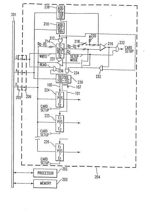
Fig. 1 is a schematic diagram of a computer system including
an adapter card of the present invention.
SUMMARY of the INVENTION
Briefly, the invention is a computer adapter card including
a bus connecting means for electrically connecting the
adapter card to a computer bus. A first data register
stores a programmable adapter card number that is received
from the bus connecting means. A first address decoder
decodes a first address that is received from the bus
connecting means and, in response to a decode of the first
address, provides a first enable signal to the first data
register. Switch means, which is manually selectable by a
user, is provided for selecting a switch selected adapter
card number. A second data register stores setup data
received from the bus connecting means, and a second address
decoder provides a second enable signal to the second data
register in response to a decode of a second address. A
comparator is provided for comparing the programmable
adapter card number stored in the first data register with
the switch selected adapter card number. When a match is
detected between the programmable adapter card number in the
BC9-91-084 4
-- 2084I33
first data register and the switch selected adapter card
number, the comparator provides a third enable signal to the
second data register. Thus, the invention operates such
that access to the seconcl data register is provided by
setting the switch means to the switch selected adapter card
number, loading the switch selected adapter card number into
the first data register, and then addressing the second data
register at the second address.
In another embodiment, the invention is a computer system
having a bus that includes an adapter card receiving means.
A processor is provided for providing address and data
information to the bus, and a memory stores a program for
execution by the processor. In addition, the computer
system includes the adapter card described in the preceding
paragraph.
DESCRIPTION of the PREFERRED EMBODIMENT
Fig. 1 is a schematic diagram of a computer system that
includes the present invention. Referring to this figure,
the computer system includes a Bus 201, a Processor 202, a
Memory 203 and an Adapter Card 204. Bus 201 is a
conventional ISA bus (or other bus that does not include
separate setup lines for each adapter card) and includes
individual control, address and data lines. Bus 201 also
includes a plurality of receptacles 205 (only one is
illustrated in Fig. 1) for receiving adapter cards, such as
Adapter Card 204. Each location at which an adapter card
can be inserted into the system i~ referred to as a "slot"
and each slot includes one receptacle 205. Each slot is
assigned a unique slot or adapter ~ard number. Although the
slot numbers may be arbitrarily assigned, they usually
correspond to the physical location of the slot. Memory 203
stores one or more programs for execution by Processor 202.
In Fig. 1, Memory 203 and Processor 202 communicate via Bus
201, although, in an ISA bus, a separate memory bus
interconnects the Memory and the Processor. The Processor
202 provides control, address and data information to Bus
201.
BC9-91-084 5
-
208~133
Adapter Card 204 is electrically connected to Bus 201 via
connector 206, which is inserted into one of the receptacles
205. Address decoder 210 is connected to the address lines
of Bus 201 and decodes I/O address port 96h (the suffix "h"
is used to indicate that the preceding number is expressed
in hexadecimal format). The output of decoder 210 is
coupled to an OR Gate 212 and the output of the OR Gate is
coupled to a First Enable input (E1) of a Data Register 214.
A Second Enable (E2) input of Data Register 214 is coupled
to the Write line of Bus 201. Both the First and Second
Enable inputs must be active in order to write data to Data
Register 214. Data register 214 has four data inputs that
are connected to the data lines of ~us 201. Three of the
four data inputs (Do~D2) to Data Register 214 are used to
write a programmable slot number into the Data Register,
while the fourth (D3) is used to indicate when the system is
in the setup mode of operation.
To write to Data Register 214, the Processor 202 places
address 96h on the Bus 201, which is decoded by Address
Decoder 210. The output of Address Decoder 210 then enables
input El to Data Register 214. During a write operation,
the Write Line of the control portion of Bus 201 is pulled
active, thereby activating input E2 of Data Register 214.
With both Enable inputs active, data bits Do -D3 are then
written into Data Register 214.
Each of the three OUtplltS Qo-Q2 ( the outputs that indicate
the programmable slot number) of Data Register 214 are
coupled to a first input of one of three Comparators 216
(only one comparator is illustrated in Fig. 1). Likewise,
each of three Switches 218 (only one switch is illustrated
in Fig. 1) is coupled to a second input of one of the
Comparators 216. Each of the second inputs to the
Comparators includes a Pull-up Resistor 220. The Switches
218 are used to select a switch selectable slot number. The
Switches 218 are manually selectable by a user and are
preferably contained in a small, eight position rotary
switch suitable for direct mounting on a printed circuit
board, although other manually selec-table switches may also
be suitable. In the a]ternative, jumpers may be used in
_ BC9-91-084 6
2084133
place of the Switches 218. The three outputs of Comparators
216 are connected to one of three inputs of a four input AND
Gate 222 (only two inputs of AND Gate 222 are illustrated in
Fig. 1). The fourth input to AND Gate 222 is connected to
the Q3 output (the output that indicates setup mode) of Data
Register 214.
After (or immediately before) inserting Adapter Card 204
into Receptacle 205, the user sets the Switches 218 to
indicate the particular slot number that the Adapter Card
has been plugged into (the switch selectable slot number).
If the programmable slot number, as loaded into bits Qo~Q2
of Data Register 214, matches the switch selectable slot
number, as selected by Switches 218, the outputs of
Comparators 216 are active. And, if Q3 (the setup mode bit
of Data Register 214) is also active, then the output (Card
Setup) of AND Gate 222 is active, indicating that Adapter
Card 204 is in the setup mode. (Note that, if the switches
of each of the adapter cards in the system are set to unique
slot numbers, then only one of the adapter cards can be
placed in the setup mode at any one time.)
The output of AND gate 222 (Card Setup) is coupled to the
Second Enable (E2) input of each of eight data registers
POSO - POS7 (only three such data registers 224, 225, and
226 are illustrated in Fig. 1). These data or "setup"
registers, which are referred to as Program Option Select or
"POS" registers, are used to store setup information
pertinent to this particular adapter card. These setup
registers correspond to the POS registers in the Micro
Channel bus version of the computer.
To individually address each one of the POS registers,
Address Decoder 230 decodes addresses lOOh through 107h, and
a decode of each address within this range causes a First
Enable (El) input of a corresponding POS register to be
enabled. For example, when address lOOh is decoded, input
El of the POSO register t224) is activated. Similarly, when
address lOlh is decoded, input E1 of the POS1 register (225)
is enabled. However, before any one of the POS registers
can be accessed, the adapter card must be placed in the
~ BC9-91-084 7
2084133
setup mode, such that Card Setup activates the Second Enable
(E2) inputs of the P0S registers.
To setup an adapter card, the processor must write setup
parameters to, and read setup parameters from the P0S
registers. The processor does this under the control of a
setup program stored in the Memory 203, which is usually run
at system initialization. Since the setup program is well
known in the Micro Channel computer art, the details of the
program are not presented here.
To write parameters to and read parameters from the P0S
registers, the Processor 202 begins by placing address 96h
on the bus, thereby selecting Address Decoder 210. The
processor then selects a particular adapter card slot by
writing a "programmable card slot number" into Data Register
214. Simultaneously with the writing of the programmable
card slot number, the processor also sets the third bit (Q3)
of Data Register 214 active to indicate that the system is
now operating in the setup mode. If the system is in the
setup mode, and if the programmable card slot number, as
stored in Data Register 214, matches the switch selectable
card number, as determined by the setting of the switches
218, each one of the P0S registers on the currently selected
adapter card may now be individually accessed. To access a
particular P0S register, the Processor places the
corresponding address of the P0S register (100h for P0S0,
101h for POS1, etc.) on the Bus. and Address Decoder 230
then enables the selected P0S register through its E1 input.
Primarily for testing purposes, it is also possible to read
the contents of Data Register 214. To permit the reading of
the contents of Data Register 214, the output of a four line
Bus Transceiver 231 is coupled to the data portion of Bus
201, and the Q0 through Q3 outputs of Data Register 214 are
coupled to the inputs of this Bus Transceiver. The output
of Comparator 216 and the output of Address Decoder 210 are
coupled to the input of a two input AND Gate 232. The
output of AND gate 232 is coupled to one input of an OR Gate
234, the output of which is coupled to one input of a two
input AND Gate 236. The other input of AND Gate 236 is
BC9-91-084 8
2084133
coupled to the Read Line ol the control portion of Bus 201.
The output of AND Gate 236 is coupled to the enable input of
Transceiver 231. Consequent]y, when the card is in the
setup mode, the output of comparator 216 and the first input
of AND Gate 232 are active. The second input of AND Gate
232 is active when Address Decoder 210 is selected by
placing address 96h on the Bus. Under both of these
conditions, the output of AND Gate 232 is active and this
signal is passed through OR Gate 234 and into the first
input of AND Gate 236. When the control portion of Bus 201
indicates that the Bus is in read mode by pulling the Read
active, the other input of AND Gate 236 also goes active.
Since both inputs of AND Gate 236 are now active, its output
goes active, thereby enabling Transceiver 231 and gating the
contents of Data Register 214 onto the Bus.
There is an additional method of reading the contents of
Data Register 214. To accomplish this, Address Decoder 238
has three inputs that are coupled to the output of Switches
218, thereby presenting the switch programmable card number
to Address Decoder 238. The other input to Address Decoder
238 is coupled to the address lines of Bus 201, such that
the Address Decoder decodes an address within the range of
108h - 10Fh. The particular address within that range that
is decoded depends upon the three inputs from Switches 218.
Consequently, when Switches 218 are set to Card Number 0,
the output of Address Decoder 238 goes active only when
address 108h is placed on the Bus. Similarly, when the
Switches are set to Card Number 1, the output of the Address
Decoder goes active only when address 109h is placed on the
Bus. This output from Address Decoder 238 is coupled to the
second input of OR Gate 234, thereby enabling Bus
Transceiver 231 when the read line of Bus 201 is active.
The output of Address Decoder 238 is also coupled to the
second input of OR Gate 212, thereby enabling the first
Enable Input El of Data Register 214 when an address in the
range of 108h - 10Fh is decoded, and when that address
corresponds to the switch programmable card number set by
Switches 218. Thus, by addressing the card in this way, a
BC9-91-084 9
~ 2084133
second method is provided for writing data into Data
Register 214.
Other embodiments are within the scope of the following
claims.