Note: Descriptions are shown in the official language in which they were submitted.
2n842~4
SPECIFICATION
Title of the Invention
JOSEPHSON JUNCTION DEVICE FORMED OF OXIDE
5 SUPERCONDUCTOR MATERIAL AND PROCESS FOR PREPARING
THE SAME
Background of the Invention
Field of the invention
The present invention relates to a Josephson junction device formed
of oxide superconductor material and a process for preparing the
Josephson junction device, and more specifically to a Josephson junction
device of an oxide superconductor, of which a barrier of the weak link is
c-)nctir~ d of a grain boundary and a process for preparing the Josephson
15 junction device.
Description of related art
A Josephson junction device wllich is one of superconducting
devices can be realized in various structures. Among the various
2 0 structures, the most preferable structure in practice is a stacked junction
realized by a thin non-superconductor layer sandwiched between a pair of
superconductors. However, a pOillt contact type junction, a Dayem bridge
type junction and a vari~ble thickness bridge type junction which are
composed of a pair of superconductor regions wllich are weakly linked to
25 each other also exhibit Josephson effect. In general, these Josephson
junctions have fine structures in which the superconductor and/or
non-superconductor are composed of thin films. ~
~ 208426~
In o}der to realize a stacked type junction by using an oxide
superconductor, a first oxide superconductor thin film, a non-
supercc)n~ ctQr thin film and a second oxide superconductor thin film are
stacked on a substrate in the named order.
In the above mentioned stacked type junction, an insulator MgO
etc., a semiconductor Si etc, and a metal Au etc. are used for the non-
superconductor layers so that each superc~n~lctin~ junction has different
properties for each application.
The thickness of the non-superconductor layer of the stacked type
junction is determined by the coherence length of the superconductor. In
general, the thickness of the non-superconductor layer of the stacked type
junction must be within a few times of the coherence length of the
superconductor. On tlle other hand, since oxide superconductor materials
have a very short coherence length, tllerefore, a thickness of a non-
superconductor layer must be about a few nanometers.
However, the superconductor layers and the non-superconductor
layer of the stacked type junction must be of high crystallinity for
favorable junction properties, which are composed of single crystals or
composed of polycrystals which are orientated in almost same direction.
2 0 It is difficult to stack an extremely thin and high crystalline
non-superconductor layer on an oxide superconductor layer.
Additionally, it is very difficult to stack a high crystalline oxide
superconductor layer on the non-superconductor layer stacked on an
oxide superconductor layer. Though the stacked structure including a
2 5 first oxide superconductor layer, a llon-s~lperconductor layer and a secondoxide superconductor layer is realized, the interfaces between the oxide
superconductor layers and the non-superconductor layer are not in good
~r
~,!,. _ ~ _
2~84264
condition so that the stacked type junctioll does not function in good
order.
In order to manufacture a point contact type junction, a Dayem
bridge type junction and a variable thickness bridge type junction by using
5 oxide superconductor, very fine processings which realize a weak link of
a pair of superconductor are necessary. It is very difficult to conduct a
fine processing with good repeatability.
The point contact type junction has been formed of two oxide
superconductor thin films wllich are in contact with each other in a
10 extremely small area whicll conslitute~ the weak lillk of the Josephson
junction.
The Dayem bridge type jU~lCtiOli has been formed of a constant
thickness oxide superconductor thil~ film which is formed on a substrate
and which is patterned in a plall view, so tllat a superconductor thin film
15 region having a greatly narrow width is formed between a pair of
superconductor thin film regions h~ving a sufficient width. In other
words, the pair of superconductor thin film regions having a sufficient
width are coupled to each other by the s~lperconductor thin film region
having the greatly narrow width. Namely, a weak link of the Josephson
20 junction in the superconductor thill film is formed at the greatly narrow
width region.
On the other hand, the variable tllicklless bridge type junction has
been formed of an oxide superconductor thin film of a sufficient thickness
which is formed on a substrate and whicll is partially etched or thinned in
25 a thickness direction, so that a thinned oxide superconductor thin film
portion is formed between a p~lir of superconductor thin film portions
having the sufficient thickness. In other words, the pair of
- 3 -
2~8426~
superconductor thin film portions having the sufficient thickness are
coupled to each other by the thinned oxide superconductor thin film
portion. Accordingly, a weak link of t'lle Josephson junction is formed at
the reduced thickness portion of the oxide superconductor thin film.
As would be understood from the above, a characteristics of the
Josephson device has a close relation to the contact area of the
superconductor thin film in the point contact type Josephson device, the
width of the superconductor thin film region having the extremely
narrow width in the Dayem bridge type Josephson device, and to the
thickness of the thinned oxide supercollductor thin film portion in the
variable thickness bridge type Josephson device, both of which form the
weak link of the Josephson junction. Therefore, in order to obtain a
desired characteristics witll a good repeatability, a high precision on a
sub-micron level of the processing such as tlle etching is required.
The Dayem bridge type Josephsoll device can be said to be more
preferable than the variable thickness bridge type Josephson device, since
the Dayem bridge type Josephson device has a relatively planer surface,
which is preferred in a integrated circuit. However, in order to for.n the
weak link in the Dayem bridge type Jos,ephson device, it is required to
pattern an oxide superconductor tllin film havillg the thickness on the
order of 0.5 ,um to 1.0 llm into a width of not greater than 0.2 llm.
However, it is very difficult to conduct tllis fine patterning with good
repeatability.
On the other halld, in the variable thickness bridge type Josephson
device, the very fine pattering is not re4uiled in order to form the weak
link. However, it is very difficull to uniformly control the remaining
thickness of the thinned portion forming the weak link. In addition, the
- 4 -
.
2~8~264
variable thickness bridge type Josepllson device cannot have a planer
surface by nature. This is not preferable to the integrated circuit
application.
Therefore, in the prior art, it is almost impossible to m~nl-fs~tllre a
5 superc-~n~ ctin~ device which has multiple homogeneous Josephson
junctions by using an oxide superconductor.
In order to resolve the above m~ntionl~d problems, so-called step
type Josephson junction device is proposed in a prior art. A Josephson
junction device of this type comprises a substrate which includes a step on
10 a principal surface and an oxide supercollductor thin film formed on the
principal surface of the substrate. The oxide superconductor thin film has
a grain boundary at the step portion so tllat tlle oxide superconductor thin
film separated two parts above ~nd below tlle step which is linked weakly
by the grain boundary. Each of the parts constitutes a supercon~ tin~
15 electrode and the grain boundary constitutes a weak link of a Josephson
junction. Thus, the above oxide superconductor thin film con~til~lte a
Josephson junction device.
No fine processing whic~l is required to manufacture a point contact
type Josephson junction device, a Dayelll bridge type Josephson junction
20 device or a variable thickness bridge type Josephson junction device is
necessary to manufacture the step type Josephson junction device.
However, crystalline directions of the two parts of the oxide
superconductor thin film sometimes becomes different from each other so
that too large interfacial energy and llnllece~s~ry electrical resistance are
2 5 generated at the step portion, which spoil the characteristics of the
Josephson junction. This difference of the crystalline directions is
208426~
considered to be caused by deformation of crystalline lattices of an etched
surfdce of the substrate.
Summary of the Invention
Accordingly, it is an object of the present invention to provide a step
type Josephson junction device composed of an oxide superconductor
material, which addresses the above m~nti-)n~d defects of the prior art.
Another object of the present invention is to provide a method for
manufacturing a Josephson junction device with good repeatability by using
already established processing techniques.
According to a first aspect of the invention there is provided a
Josephson junction device comprising a single crystalline substrate
including a principal surface, an oxide layer formed on the principal surface
of the substrate having a step in its upper surface, and oxide superconductor
thin films and oxide thin films alternately formed on the upper surface of
the oxide layer. The thickness of each of the oxide sup~r~-)nlll-~ t--r thin
films and each of the oxide thin films is the same and each oxide
superconductor thin film includes a step with a first and a second portion of
the oxide superconductor thin film respectively positioned above and below
the step. The first and second portions of the oxide superconductor thin
film are constituted of single crystals of the oxide ~uL~ ductor having an
identical crystal orientation, and a grain boundary is provided on the step of
the oxide layer which constitutes a weak link of the Josephson junction.
--6 --
Bi
2084264
In a preferred embodiment, the oxide thin film is formed of
Prl Ba2Cu3O7 y oxide.
In a preferred embodiment, the oxide superconductor thin film is
formed of high-TC (high critical temperature) oxide superconductor,
5 particularly, formed of a high-TC copper-oxide type compound oxide
superconductor for example a Y-Ba-Cu-O compound oxide superconductor
material, a Bi-Sr-Ca-Cu-O compound oxide superconductor material, and a
Tl-Ba-Ca-Cu-O compound oxide superconductor material.
It is preferable that the height of the step of the oxide layer is the same
10 as the thickness of the oxide superconductor thin film and oxide thin film.
In this case, the adjoining oxide superconductor thin films can constitute
Josephson junctions.
According to another aspect of the present invention, there is
provided a method for manufacturing a Josephson junction device
15 comprising the steps of forming an oxide layer on a principal surface of the
single crystalline substrate, etching a portion of the oxide layer so that a step
is formed on the surface of the oxide layer, forming an oxide
superconductor thin film on the surface of the oxide layer and an oxide thin
film having the same thickness as th~t of the oxide superconductor thin
20 film on the oxide superconductor thin film and repeating forming oxide
superconductor thin films and oxide thin films so that the oxide
superconductor thin films and oxide thin filrns are stacked alternately and
eachof the oxide superconductor thin films includes a first and a second
- 7--
B~
208~2~
portions respectively positioned above and below the step of the oxide layer,
which are constituted of single crystals of the oxide superconductor, and a
grain boundary between every pair of said upper and lower portions, which
constitutes a weak link of the Josephson junction
In one preferred embodiment, the step of the oxide layer is formed so
as to have the same height as the thickness of the oxide superconductor
thin films and oxide thin films.
The above and other objects, features and advantages of the present
invention will be apparent from the following description of preferred
embodiments of the invention with reference to the accompanying
drawings.
Brief Description of the Drawings
Figures lA to lD are diagrammatic views for illustrating a first
embodiment of the process for manufacturing the Josephson junction
device;
Figures 2A to 2G are diagrammatic views for illustrating a second
embodiment of the process for manufacturing the Josephson junction
device in accordance with the prese~ vention.
B
208~264
Description of the Preferred embodiments
Referring to Figures lA to lD, a first embodiment of a process for
mAn1lfArhlrin~ a Josephson de~ice will be described.
As shown in Figure lA, an MgO (100) single crystalline substrate 1
5 having a s11hstAn~iAIIy planar principal surface ((100) surface) was prepared.
In this embodiment, the MgO substrate had a size of 15 mm x 8 mm and a
thickness of 0.5 mm. The MgO substrate 1 was heated to a L~ dLul~ of
1100C under 2 atmosphere for 8 hours in order to clean its surface. This
heat-treatment was not necessary, if the surface of the MgO substrate 1 was
10 clean enough.
Then, as shown in Figure lB, a Pr1Ba2Cu3O7y oxide layer 3 having a
thickness of 200 nanometers was formed on the MgO substrate 1 by a
sputtering. The ronfli~if)n~ of the sputtering process were as follows;
Icm~e _
g
B~
2084264
Sputtering gases A r 9 sccm
2 I sccm
Pressure 5 x 10⁻² Torr
The PrlBa2Cu3O7 y oxide layer 3 can also be formed by an MBE
(molecular beam epitaxy), a vacuum evaporation, a laser ablation, etc.
Thereafter, as shown in Figure I C, a portion 32 of the
PrlBa2Cu3O7 y oxide layer 3 was etched by an ion milling using Ar ions
so as to form a step 33. The step 33 llad a height of 150 n~nl-m~Prs. The
PrlBa2Cu3O7 y oxide layer 3 can be etched by a reactive ion etching or
wet etching. In this connection, tlle etched portion 32 of the
PrlBa2Cu3O7 y oxide layer 3 should have a thickness t thicker than 10
ns~nom~t~rs. After the etching, the substrate I was heated up to 350 to
400 C under a pressure lower tllan I x 10-9 Torr to clean up the surface
of the PrlBa2Cu3O7 y oxide layer 3. This heat-treatment was not
necessary, if the surface of the PrlBalCu3O7 y oxide layer 3 was clean
enough.
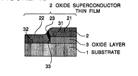
Thereafter, as sllown ill Figule I D, a YIBa2cu3o7-x oxide
superconductor tllin film 2 having a thickness of 200 nanometers was
deposited over the Pr]Ba2Cu3O7 y oxide layer 3 by a sputtering process.
The conditions of the sputtering process wele as follows;
Temperature of substrate 700C
Sputtering gas Al 9 sccm
2 1 sccm
Pressure 5 x 10⁻² Torr
2 5 The YIBa2cu3o7-x oxide superconductor thin film 2 can be formed
by an MBE (molecular beam epitaxy~, a vacuum evaporation, a laser
ablation, etc.
j-
- 10-
2084264
The Y1Ba2Cu307 x oxide superconductor thin film 2 had a grain
boundary 23 on the step 33 of the Pr1Ba2Cu307 y oxide layer 3, which
Li~uL~:d a weak link of a Josephson junction. Two parts 21 and 22 of oxide
superconductor thin film 2 which are positioned on a portion 31 and an
5 etched portion 32 of PrlBa2Cu307 y oxide layer 3 ~ supert l-n~ fting
electrodes which were linked weakly by the grain boundary. The two parts 21
and 22 of oxide superconductor thin film 2 were formed of single crystalline
Y1Ba2Cu307 x oxide superconductor of which crystalline directions were the
same as each other.
The Y1Ba2Cu307 x oxide superconductor thin film 2 could be etched so
as to form the narrow portion between portions 21 and 22, the center of
which the grain boundary 23 crossed. Metal electrodes might be formed on
the portions 21 and 22, if necessary. With this, the Josephson junction device
in accordance with the present invention was completed.
A current-voltage characteristic of the above m~ntionf~d Josephson
junction device was measured at a l~ ur~ of 85K. When a microwave
was irradiated, clear Shapiro steps were observed, and therefore, it could be
ascertained that the Josephson junction was realized in the device.
The Josephson junction device m~nllf~-~hlred in accordance with Figs.
lA to lD is composed of two super. onflllftin~ electrodes of single-crystalline
oxide superconductor, which grow at the same time and form a sheet of the
oxide superconductor thin film and which have the same crystalline
direction as each other, and a weak link of a grain boundary between
them. The weak link of the Josephson junction device is formed of a self-
-11 -
20842~
generated grain boundary. Accordingly, the limitation in the fine processing
technique required for manufacturing the Josephson junction device is
relaxed.
Referrmg to Figures 2A to 2G, a process for mAnl1f~rhlrin~ a Josephson
5 junction device according to the invention will be described.
As shown in Figure 2A, an MgO (100) substrate 1 having a size of
15 mm x 8 mm and a thickness of 0.5 mm, similar to that of Embodiment 1
was prepared. As shown in Figure 2B, a PrlBa2Cu307 y, having a thickness 50
nAnomPtPr~, was formed on the substrate 1 by an MBE process. The
0 I~nrlitit~n~ of the MBE process were as follows;
T~ 1LU1~ of substrate 750C
Oxidation gas 03 8%
2 92%
Pressure 1 x 10⁻⁵ Torr
Thereafter, as shown in Figure 2C, a portion 32 of the Pr1Ba2Cu3O7 y
oxide layer 3 was etched by an ion milling using Ar ions so as to form a step
33. The step 33 had a height of 25 nAnomPtPrc The height of the step 33 was
substantially same as the thickness of oxide superconductor thin films and
oxide thin films which would be formed on the PrlBa2Cu3O7 y oxide layer 3.
20 The Pr1Ba2Cu3O7 y oxide layer 3 can be etched by a reactive ion etching or wet
etching. The etched portion 32 of the Pr1Ba2Cu3O7 y oxide layer 3 had a
thickness of on the order of 20 nAnomPtPr~
Then, as shown in Figure 2D, a first YlBa2Cu307 ,~ oxide
superconductor thin film 211 having a thickness of 25 n~n~mPtPr~ was
- 12-
208~264
deposited over the PrlBa2Cu3O7 ~ oxide layer 3 by an MBE process. The
cnn~1itinn~ of the MBE process were as follows;
Temperature of substrate 700C
Oxidationgas O3 8 %
2 92 %
Pressure 1 x 10⁻⁵ Torr
Then, the Y molecular beam source was exchanged to a Pr
molecular beam source so that a first oxide thin film 311 composed of
PrlBa2Cu3O7 y oxide having a thickness of about 25 nanometer was
10 continuously formed on the YlBa2Cu3O7 x oxide superconductor thin film
211, as shown in Ficure 2E. Tl~e conditions of the MBE process were as
follows;
Temperature of substr~te 700C
Oxidationgas O3 8 %
2 92 %
Pressure I x 10-5 Torr
Thereafter, the Pr molecular beam source was exchanged to a Y
molecular beam source so tll~lt a second YlBa2cu3o7 x oxide
superconductor thin film was colltilluously formed on the fi}st
2 0 PrlBa2Cu3O7 y oxide thin film 311.
The above operation was repeated so that n layers of YlBa2cu3o7-x
oxide superconductor thin films 211 to 21n alld n layers of PrlBa2Cu3O7 y
oxide thin films 311 to 31n were stacked ,llternately on one another, as
shown in Figure 2F. Tlle PrlBa2Cu3O7 ), oxide thin film 31n which was
2 5 formed at the top wa~ a protection. In this embodiment, 10 YlBa2CU37-x
oxide superconductor thin films alld PrIBa2Cu3O7 y oxide thin films were
stacked. Metal electrodes might be formed on the YlBa2Cu3O7 x oxide
~r -13-
2084264
superconductor thin film 21n and 22n, if necessary. With this, the
Josephson junction device in accordance with the present invention was
completed.
In above Josephson junction device, each YIBa2cu3o7-x oxide
5 superconductor thin film has a grain boundary at its step portion which
constitutes a Josephson junction. These Josephson junctions are
constituted of self-generated grain boundaries so that they have
substantially the same char~cteristics each other. Therefore, the
Josephson junction device has integrated mu~tiple homogeneous Josephson
1 0 junction.
In addition, the adjoinillg YIBa2Cu3O7 x oxide superconrl~lctc-r thin
films also constitutes Josephsol~ junctiol~s. Referring to Figure 2G, this
will be described. Figure 2G shows an equivalent structure of the
Josephson junction device shown ill Figule 2F. As shown in Figure 2G,
15 the Josephson junctioll device is collsidered to be constituted of
Y~Ba2Cu3O7 x oxide superconductor thill films and PrlBa2Cu3O7 y oxide
thin films which are arr~nged ill rows in staggered fashion. In the
Josephson junction device, Y~B~2Cu3o7-x oxide superconductor thin film
21i constitutes one Josephson junction with YlBa2cu3o7-x oxide
20 superconductor thin film 22i and another with YIBa2cu3o7-x oxide
superconductor thin film 22i+]. Tlle oxide superconductor thin film 22i
has a weak link with the oxide supelconductor thin film 21i, because they
are grown at tlle same time to forln a step junction. However, the oxide
superconductor thill film 21i h~ls tlle same relation with the oxide
25 superconductor thin film 22i+] as the tlle oxide superconductor thin film
22i, since the oxide thin films 31i and 32i are extremely thin at the step
portions. Therefore, the oxide superconductor tllill films 22i+1 and 21i
~r - 14-
..~,
208~264
can directly contact each other throLlgh weak lil1k portion. Utilizing an
MBE method, it is possible conduct this sharp edge thin film deposition.
A current-voltage characteristics of the above mPntil-n!~d Josephson
junction device was measured at a temperature of 85K. When a
microwave was irradiated, clear Shapiro steps were observed, and
therefore, it could be ascertained that the Josephson junction was realized
in the device.
As explained above, the Josephson junction device m:lnllf~ctllred in
accordance with the second embodimel1t of the method of the present
invention includes multiple homogel1eous Josephson junction. The weak
links of the Josephson junction device are formed of a self-generated
grain boundaries. Accordil1gly, tlle limitation in the fine processing
technique required for manufacturil1g tlle Josephson junction device is
relaxed.
In addition, in the Josephson junction device, the adjoining oxide
superconductor tllin films also constitutes Josephson junctions. Therefore,
the number of Josephsol1 junctions of tlle Josephson junction device is
almost twice as much as th.lt of tlle oxide superconductor thin films.
Thus, the Josephson junction device has a l~lrge current capability.
2 0 .In the above mentioned embodiments, the oxide superconductor thin
film can be formed of not only tlle Y-Ba-Cu-O compound oxide
superconductor material, but also a high-TC (high critical temperature)
oxide superconductor material, partic~llarly a high-TC copper-oxide type
compound oxide supercol1ductor material, for example a Bi-Sr-Ca-Cu-O
2 5 compound oxide superconductor material, and a Tl-Ba-Ca-Cu-O
compound oxide superconductor materi.ll.
- 15 -
208~26~
The invention has tllus beell sllown and described with reference to
the specific embodiments. However, it should be noted that the present
invention is in no way limited to the details of the illustrated structures
but converts and modifications may be made within the scope of the
5 appended claims.
- ]6 -