Note: Descriptions are shown in the official language in which they were submitted.
-
SPECIFICATION
208427~
Title of the Invention
METHOD FOR MANUFACTURING A JOSEPHSON JUNCTION DEVICE
HAVING WEAK LINK OF ARTIFICIAL GRA~ BOUNDARY
Ba.k~..,ulld of the Invention
Field of the Invention
The present invention relates to a method for m~nl1f~ftl-rin~ a
Josephson junction device having weak link of artificial grain boundary,
5 and more specifically a Josephson junction device of an oxide
superconductor, in which the barrier of the weak link is constituted of a
grain boundary by two single crystal oxide superconductor regions.
Description of related art
A Josephson junction device which is one of sUper~ -n~ rtin~ devices
can be realized in various structures. Among the various structures, the
most preferable structure in practice is a stacked junction realized by a thin
non-superconductor layer sandwiched between a pair of super~nn-lllrtflr~
However, a point contact type junction, a Dayem bridge type junction and a
15 variable thickness bridge type junction which are composed of a pair of
superconductor regions which are weakly linked to each other also exhibit
Josephson effect. In general, these Josephson
~L
Ri
~ 2~84272
JUnCtiOnS have fine structures in whicll tlle superconductor and/or
non-superconductor are composed of thin films.
In order to realize a stacked type junction by using an oxide
superconductor, a first oxide superconductor thin film, a non-
S ~u~ JIlçtor thin film and a second oxide supercon~l~rtor thin film arestacked on a substrate in the named order.
In the above m~ntinn. d stacked type junction, an insulator MgO
etc., a sPm;c~-n~lctor Si etc., and a metal Au etc. are used for the non-
superconductor layers so tllat each superc~-nductill~ junction has different
0 ~l~JpC-ti~s for each applications.
The thickness of the non-superconductor layer of the stacked type
junction is determined by tlle collerence length of the sUperc~n~ rtQr. In
general, the thickness of tlle non-sL,~cl.;u-~ductor layer of the stacked type
junction must be within a few times of the coherence length of the
15 ~ rtç~r~ Since oxide supelconductor materials have a very short
coherence length, therefore, a thickness of a non-superconductor layer
must be about a few nanollleters.
However, the supelconductor layers and the non-superc~-n~ çtQr
layer of the stacked type junction must be of high crystallinity for
20 favorable junction properties, which are composed of single crystals or
composed of polycrystals which are orientated in almost same direction.
It is difficult to stack an extremely thin and high crystalline
non-superconductor layer on an oxide superconductor layer.
Additionally, it is very difficult to stack a high crystalline oxide
25 superconductor layer on the non-superconductor laye} stacked on an
oxide superconductor layer. Tllough the stacked structure including a
first oxide superconductor ~ayer, a noll-superc~ nd~lçt~r layer and a second
- 2 -
~ 2~8~272
oxide superconductor layer is reali~ed, the interfaces between the oxide
superconductor layers and the noll-superconductor layer are not in good
condition so that the stacked type junction does not function in good
order.
S In order to m~nllf~ctllre a point contact type junction, a Dayem
bridge type junction and a variable thickness bridge type junction by using
oxide superconductor, very fine processings which realize a weak link of
a pair of superconductor ale necessary. It is very difficult to conduct a
fine processing with good repeatability.
The point contact type junction has been formed of two oxide
superconductor thin films whicll are in contact with each other in a
extremely small area wllich constitutes the weak link of the Josephson
~unction.
The Dayem bridge type junction has been formed of a constant
thickness oxide supercnn~ t~r thin film which is formed on a substrate
and which is patterned in a plan view, so that a supercond~c~lr thin filtn
region having a greatly narrow width is formed between a pair of
superconductor thin film regions having a sufficient width. In other
words, the pair of superconductor thin film regions having a sufficient
width are coupled to eacll othel by the superconductor thin film region
having the greatly narrow widtll. Namely, a weak link of the Josephson
junction in the superconductor thin film is forllled at the greatly narrow
width region.
On the other hand, tlle variable thickness bridge type junction has
2 5 been formed of an oxide superconductor thin film of a sufflcient thickness
which is formed on a substrate and which is partially etched or thinned in
a thickness direction, so that a thinned oxide superconductor thin film
- 3 -
~ 208~272
portion is formed between a pair of superconductor thin film portions
having the sufficient thickness. In other words, the pair of
superconductor thin film portions having the sufficient thickness are
coupled to each othe} by the thinned oxide superconductor thin film
S portion. Accordingly, a wea~ link of the Josephson junction is formed at
the reduced thickness portion of the oxide superc~n~lctor thin filrn.
As would be understood from the above, a characteristics of the
Josephson device has a close relation to the contact area of the
superconductor thin fiLm in the point contact type Josephson device, the
10 width of the supercond~lctor thin film region having the extremely
narrow width in the Dayem bridge type Josephson devicet and to the
thickness of the thinned oxide superconductor thin film portion in the
variable thickness bridge type Josepllson device, both of which form the
weak link of the Josephson junction. Therefore, in order to obtain a
15 desired clld-d.,-Le~ ics wi~h a good repeatability, a high precision on a
sub-micron level of the processing such as the etching is required.
The Dayem bridge type Josephson device can be said to be more
preferable than the variable tllickness bridge type Josephson device, since
the Dayem bridge type Josephson device has a relative~y planer surface,
- 2 0 which is preferred in a integrated circuit. However, in order to form the
weak link in the Dayem bridge type Josepllson device, it is required to
pattern an oxide superconductor thin film having the thickness on the
order of 0.5 ~lm to 1.0 llm into a wid~h of not greater than 0.2 llm.
However, it is very difficult to conduct this fine patterning with good
2 5 repe~t~ ility.
On the other hand, in tlle variable thickness bridge type Josephson
device, the very fine pattering is not req~ired in order to form the weak
- 4 -
~8~272
link. However, it is very difficult to uniformly control the remaining
thickness of the thinned portion forming the weak link. In addition, the
variable thickness bridge type Josephson device cannot have a planer
surface by nature. This is not preferable to the integrated circuit
5 application.
Therefore, in the prior art, it is almost impossible to m~mlf~rt~lre a
superconducting device for example a dc SQUID (superc~nd~ tin~
quantum i~lLC~r~ ce device) which has multiple homogeneous Josephson
junctions utilizing an oxide superconductor.
In orde} to resolve the above m~nti~n~d problems, ~s~ es have
been c--ntlll~ d to ~ ,lr~t~ re a Josephson junction device taking account
of the characteristics advantage intrinsic to the oxide superconductor,
p~ Li-lg it to avoid tlle fine processing of tlle oxide superconductor.
The superconducting characteristics of the oxide superconductor
15 considerably varies, depending Oll the crystalline direction. Particularly,
the oxide superconductor llas a large critical current density in the
direction perpendicular to the c-axes of its crystals. Thus, if the oxide
superconductors having crystalline directions different from each other
are joined together, a grain boundary at the interface becomes a barrier
20 of the weak link so that a Josephso1l junction is formed. A Josephson
junction device utilizing tllis Josepllson junction is called artificial grain
boundary type Josephson junction device. A Josephson junction device of
this type can be manufactured witllout the fine processing as m~nti~n~d
above.
2 5 In order to manufacture the artificial grain boundary type
Josephson junction device, in a prior art, the same two substrates were
joined so as to form a substrate of which the crystalline directions of each
- 5 -
' 2084272
sides were different from each other. Then, an oxide supereonduetor thin
film was deposited thereon so as to form an oxide superconductor thirl
film having different crystalline directions in both sides. However,
aceording to the process, it was difficult to join the substrates having
S different crystalline directions and particularly the junction interfaee was
not sharp so that the artifieial barrier forming the weak link of the
Josephson junetion device could not be formed sharply.
In another prior art, a specific buf~`er layer was formed on a
portion of the substrate and an oxide supercondueto} thin film was
10 deposited thereon. A portioll of tlle oxide superconduGtor thin film whieh
grew on the buffer layer had ~ clyst.llline orientation different from that
of the other portion of the oxide superconductor thin fi~m which grew
directly on the substrate. 11l tllis process, tl~ere are very few buffer layer
materials which have these characteristics and which does not affect the
15 oxide superconductor at all. In ~dditioll, buffer layer patterning proeess
might affect the principal surface of the substrate on which the oxide
superconductor thin film is deposited.
Summary of the Invention
Accordingly, it is an object of the present invention to provide a
method for manufacturing a Josephson junction device with good
repeatability by using already established processing techniques.
Another object of tlle presellt illvention is to provide a method for
25 manufacturing a Josephson junction device with good repeatability by
using already established processillg techniques.
-6 -
R~
20842~2
A Josephson junction device may comprise a
single crystalline substrate including a principal surface
having a first and a second regions of which at least lattice distance of
exposed lattices are slightly different from each other, and an oxide
superconductor thin film fommed on the p~incipal surface of the substrate,
which includes a first and a second portions respectively positioned on the
first and the second regions of the substrate, which are constituted of
single crystals of the oxide superconductor, lattices of the one shifts at
angle of 45; to that of the other and a grain boundary between said two
portions, which constitutes a weak lillk of the Josephson junction.
In a preferred embodiment, the oxide superconductor thin film is a
c-axis orientated oxide superconductor thin film. In this case, the a-axes
and the b-axes of the oxide superconductor crystals which constit~lt~ the
first portion of the oxide superconductor thin film shifts at an angle of
45 to those of the second portion of the oxide superconductor thin film.
In a preferred embodiment, a step is formed on the principal
surface of the substrate between tlle first ~nd second regions. In this case,
the grain boundary which constitutes tlle weak link of Josephson junction
is positioned at the step portion.
2 o The substrate is preferably formed of MgO and it is preferable that
the Josephson junction device further comprises SrTiO3 buffer layer
which constitutes one of the first and second regions of the principal
surface of the substrate.
In a preferred embodiment, t~le oxide superconductor is formed of
2~ high-Tc (high critical temperature) oxide superconductor, particularly,
formed of a high-TC copper-oxide type compound oxide superconductor
- 7 -
2084272
for example a Y-Ba-Cu-O compound oxide superconductor material, a Bi-Sr-
Ca-Cu-O compound oxide superconductor material, and a Tl-Ba-Ca-Cu-O
compound oxide superconductor material.
According to the present invention, there is provided a method for
manufacturing a Josephson junction device comprising the steps of:
wet-etching at least a portion of a principal surface of a single
crystalline substrate so that the principal surface includes a first and a second
region, of which at least a lattice distance of an exposed lattice of said firstregion is slightly different from a lattice distance of an exposed lattice of said
second region, and
forming an oxide superconductor thin film on the first and second
regions of the principal surface so that the oxide superconductor thin film
includes first and second portions respectively positioned on the first and
the second regions of the substrate, said first and said second portions of saidoxide superconductor thin film being constituted of single crystals of the
oxide superconductor, wherein a lattice of said first portion is oriented at an
ang~e of 45 to a lattice of the second portion, and so that the oxide
superconductor thin film has a grain boundary between said first and second
portions, which constitutes a weak link of the Josephson junction.
The substrate is preferably formed of MgO single crystalline substrate,
since the lattice distance of MgO crystals varies when they are wet-etched by
HC1 or H3PO4.
In a preferred embodiment, the method comprises steps of wet-
etching a portion of the principal surface of the substrate so as to form a step,
a first and a second regions of which lattice distance of exposed lattices are
slightly different from each other at the both sides of the step.
In another preferred embodiment, the method comprises steps of
wet-etching the principal surface of the substrate, dry-etching a portion of
the wet-etched principal surface in order to remove a surface of thc
- 8 -
12
~ 2~84272
portion so as to forln a first alld a second regions on the principal surface
of the substrate, of which lattice distance of exposed lattices are slightly
different from each other.
In still another preferred embodiment, the method comprises the
5 steps of etching a portion of a principal surface of MgO single crystal
substrate so as to form a step, forming a layer of material other than MgO
which can be a base of an oxide supercon~ ctor thin film only at a portion
below the step so that the principal surface is substantially planarized,
wet-etching the principal surface of the substrate so as to form a first and
10 a second regions of which lattice distance of exposed lattices are slightly
different from each other.
The above and other objects, features and advantages of the present
invention will be apparent fronl tlle following description of preferred
embodiments of the invention with reference to the accompanying
1 5 drawings.
Brief Description of the Drawings
Figures lA to ID are diagramrnatic views for illustrating a first
embodiment of the process for mamJfacturing the Josephson junction
2 ~ device in accolJa-lc~ with the present invention;
Figures 2A to 2F are diagrammatic views for illustrating a second
embodiment of the process for m~n~1f~i~tllling the Josephson junction
device in accordance with the present invention; and
F;gures 3A to 3F are diagrammatic views for illustrating a third
25 embodiment of the process for manufacturing the Josephson junction
device in accordance with the presellt invention.
~ 2084272
Description of the Preferred embodiments
Embodiment 1
Referring to Figures lA to lD, a first embodiment of the process in
accordance with the present invention for manufacturing the Josephson
device in a~ d~ with tlle present inventioll will be described.
As shown in Figure lA, an MgO (100) sing}e crystalline substrate 5
having a sllbstAntially planar principal surface ((100) surface) was
prepared.
Then, a ~eft half portion of tlle principal surface of the MgO~100)
10 substrate 5 was wet-etched by H3PO4 so as to form a step portion 53, as
shown in Figure lB. Tlle step portion 53 had a height of not less than 50
nAnnm~t~rS After the etching, the lattices distance of MgO crystals
exposed on the surface of the wet-etched legion 52 of the principal
surface of the substrate 5 was slight~y changed in such a way that a thin
15 film having a different crystalline direction from that of the MgO crystals
was able to grow epitaxialiy on the region 52.
Thereafter, as showll in Figure lC, in order to elimin~t~
C-~,)IA,,,i,,Alinn adhered to the region S1, the substrate 5 was irradiated by
Ar ions obliquely from the side of the region 51 of the principal surface
20 of the substrate 5. The Ar iOllS were irradiated at an angle as shallow as
possible so that the surface of the region 52 was not etched. Then, the
substrate 5 was heated up to 350 to 400 'C under a pressure lower than 1
9 Torr to clean up the regions 51 and 52 of the substrate 5.
Thereafter, as shown in Figure lD, a YIBa2cu3o7 x oxide
25 superconductor thin film ~ having a thickness of 30û nanometers was
deposited over the regions 51 and 52 of the substrate 5 by a b~ lg
process. The conditions of the sputtering process were as follows;
- 10 -
2084272
Temperature of substrate 700C
Sputtering gas Ar 9 sccm ~gO%)
O~ 1 sccm (10%)
Pressure 7.5 x 10⁻² Torr
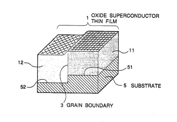
The ~-axes and b-axes of lattices of a portion 12 of the c-axis
orientated YIBa2cu3o7~x oxide superconductor thin film 1, which grew on
the wet-etched region 52 shifted at angle of 45 to those of a portion 11 of
the Y1Ba2Cu3O7 x oxide superconductor thin film 1, which grew on the
rlon-etched region 51. A grain boundary 3 was created at the interface
1 0 between the portions l l and 12, which was just on the step portion 53.
The portions 11 and 12 of the Yl~a2Cu3O7.x oxide superconductor thin
film 1 were linked weakly by the grain boundary 3 so that the Josephson
junction, where the supercond~lctill~ electrodes were cn~ d of the
portions 11 and 12 of the YIBa2cu3o7 x oxide superconductor thin film 1
and the weak link was constituted of the grain boundary 3, was formed.
The YIBa2Cu3O7 x oxide superconductor thi~ film 1 could be etched so as
to form the narrow portion between portions 11 and ~2, the center of
which the grain boundary 3 crossed. Meta~ electrodes might be forrned
on the portions 11 and 12, if necessary. With this, the Josephson junction
2 0 device in accol~l,ce with the present invention was completed.
A current-voltage Cl~ .;Lt. i~liCS of the above m~nti~nPd Josephson
junction device was measured at a temperature of 85K. When a
microwave was irradiated, clear Shapiro steps was observed, and
therefore, it could be ascertained that the Josephson junction was realized
2 5 rn the device.
As e~plained above, the Josephson junction device m~n~f~ctllred in
accordance with the first embodiment of the method of the present
I I
~ 2~8~272
invention is composed of two superconducting electrodes of
single-crystalline oxide superconductor, which grow at the same time and
form a sheet of the oxide superconductor thin film and which have a
crystalline direction different at angle of 45~ from each other, and a weak
5 linl~ of a grain boundary between tllem. Tlle weak ~ink of the Josephson
junction device is formed of a self-generated grain boundary.
According~y, the limitation in the fine processing t~rhnif~ required for
",~ ,r~l".;"~ the Josephson junctiorl device is relaxed.
10 Embodiment 2
Referring to Figures 2A to 2F, a second embodiment of the process
for ",~""r~ ,g the supercon-lllctin~ device will be described.
As shown in Figure 2A, an MgO (100) substrate similar to that of
Embodiment I was prepared. In this embodiment the MgO (100)
15 substrate had a size of 15 mm x 8 Inm alld a thickness of 0.5 mm. As
shown in Figure 2B, a mask ~ayel- 8 of PrlBa2Cu307.y, gllffici~ntly thick,
for exarnple, having a thicklless of about 750 to 1500 nanometers, was
fonned on the substrate 5 by a spuitering process. The conditions of the
D~ulL~ lg process were ~s follows;
Tc;llll~ldlul~ of substrate 75ûC
Sputtering gas Ar 9 sccm (90%)
2 1 sccm (10%)
Pressure 5 x 10⁻² Torr
Thickness of film 800 n~ om~t~rs
The mask ~ayer 8 can be formed of any material which can
cr~ngt;tlJtP an effecti~e mask against ion beam etching. For example, Nb is
pl~ F, other than PrlBa2Cu3O7-y-
- 12-
~ 208~272
Then, as shown in Figure 2C, a cellter portion of the PrlBa2Cu3O7.y
mask layer 8 was removed by an ion milling using Ar-ions so that a
portion of the surface 50 having a width of 3.0 I~lm was exposed at the
center of the substrate S and mask layers 81 and 82 were arranged at the
5 both sides of the exposed surface 50.
Thereafter, as shown in Figure 2D, the exposed surface 50 of the
substrate was wet-etched about 50 nqnometPr~ thick from the surface by
H3PO4. By this etching process, the lattice distance ~f MgO crystals
exposed on the surface 50 of the substrate 5 was slightly changed in such a
10 way that a thin film having a different crystal~ine direction from that of
the MgO crystals was able to grow epitaxially on the reg;on 50.
Then, as shown in Figure 2E, a portion 51 of the region 50 was
etched by a dry etching process using an Ar ion beam so that MgO
crystalline latices which were not affected by the wet-etching were
l S exposed. In order to remove the surface portion of only the portion 51,
the Ar ion beam was irradiated so as to form an angle ~ of 30 with
respect to the su~face of the substrate. It is preferred that the incline
angle ~ of the ion beam is adequately determined by the thickness of the
formed mask layers 81 and 82 and the border line portion between the
2 0 portions 51 and 52.
Then, the substrate 5 was lleated at a L~ Ul~ of 350 to 400 C
for one hour under a l~igh vacuum of about 1 x 10-l ~orr so as to clean
the surface portions 51 and 52 of the substrate 5. Thereafter, a c-axis
orientated YIBa2cu3o7~x oxide superconductor thin film 1 having a
25 thickness of 250 nqnomet~rs was deposited on the substrate 5 by a
sputtering. ~he cfln(iition~ of the sputtering were as follows;
.,.alulc of substrate 700C
- 13 -
2084272
Sputtering gas Ar 9 sccm (90%)
2 1 sccm (10%)
Pressure 5 x 10⁻² Torr
The direction of crystalline lattices of a portion ll of the c-axis
5 orientated YIBa2Cu3o7-x oxide superconductor thin film 1 coincided with
that of the ~gO crystalline lattices of the substrate 5. On the cont}ary,
the a-axes and b-axes of lattices of a portion 12 of the c-a~is oriPnt~t~d
YlBa2CU37-x oxide superconductor thin film 1, which grew on the
portion 52 shifted at angle of 45 to those of the portion 11 of the
10 YIBa2cu3o7-x oxide superconductor thin film 1, as shown in Figure 2F.
A grain boundary 3 was created at the interface between the portions 11
and 12, which was just on the step portion 53. The portions 11 and 12 of
the YIBa2Cu3O~ x oxide superconductor thin filn~ I were linked weakly by
the grain boundary 3 so tllat the Josephson junction, where the weak link
15 was cc~ d of the grain boundary 3, was formed. The YIBa2Cu3O7.x
oxide superconductor thin film I could be etched so that the narrow
portion, on the center portion of which the grain boundary 3 was
positinn-o-i, was created betweell portions 11 and 12. Metal electrodes
might be formed on the portions 11 and 12, if necessary. With this, the
20 Josephson junction device in accordance with the present invention was
completed.
A current-voltage characteristics of the above m~nti~nPd Josephson
junction device was measured at a temperature of 85K. When a
microwave was irradiated, clear Shapiro ste~s was observed, and
2 5 therefore, it could be ascertained that the Josephson junction was realized
in the device.
- 14-
~ ~g~272
As explained above, the Josephson junction device m~n-lf:~rt lred in
accordance with the second embodiment of the method of the present
invention is composed of two superconducting electrodes of
single-crystalline oxide ~u~el~onductor, which grow at the same time and
5 forrn a sheet of the oxide superconductor thin film and which have a
crystalline direction different at angle of 45 from each other, and a weak
link of a grain boundary between them. The weak link of the Josephson
~unction device is formed of a self-generated grain boundary.
Accordingly, the limit:l~ion in the fine processing technique required for
10 ~ ",r~ l",i~g the Josephson junction device is relaxed.
F.m~o~imPnt 3
Referring to Figures 3A to 3F, a third embodiment of the process
for manufacturing the supercon~ tin~ device will be described.
As shown in Figure 3A, an MgO (100~ substrate 5 having a size of
15 mm x 8 mm and a thickness of 0.5 mm, similar to those of
P.mborlim~nts 1 and 2 was prepared.
Then, as shown in Figure 3B, after covering a part of the substrate
5 with a photoresist 7, tlle substrate 5 was etched by an ion millin~ so that
2 0 a step 53 having a height of 200 nanometers was formed.
Thereafter, as shown in Figure 3C, tlle substrate 5 was cleaned up
by a reverse sputtering process and a SrTiO3 thin film 4 having a
thickness of 300 nanometers was deposited on the whole surface of the
substrate 5 by a sputtering. The conditions of the sputtering were as
2 ~ follows;
Temperature of substrate 350'C
Sputtering gases Ar 9 sccm
- 15 -
~ 2084272
Pressure 5 x 10⁻² Torr
The direction of crystalline lattices of the SrTiO3 thin film 4
c~inciA~d with that of MgO crystalline lattices of the substrate 5.
Then, as shown in Figure 3D, the whole surface of the substrate 5
S was etched baclc by an ion milling process so that the surface was
planari~ed. By this, two regions, that is, a region in which MgO (100)
surface was directly exposed and a region covered with the SrTiO3 layer
40 were formed on the surface of the substrate 5.
Thereafter, as shown in Figure 3E, tlle whole surface of the
10 substrate 5 with the SrTiO3 layer 40 was wet-etched by H3PO4. This
etching process was limited to the wet-etching process and the surface of
the substrate S was etched more than 50 n~nnm~t~rs thicl~. By this etching
process, the lattice distance of MgO crystals exposed on the surface 52 of
the substrate 5 was changed in such a way that a thin film having a
15 different crystallir~e direction fiom that of the MgO crystals and also the
SrTiO3 layer 40 was able to grow epitaxially on the region 52.
Finally, as shown in Figure 3F, a YIBa2cu3o7-x oxide
superconductor thin film I having a thickness of 300 nanometers was
deposited on the substrate 5 by a sputtering. The conditions of the
2 0 ~posi~inn were as follows;
T~ IJIC o~ substrate 700~C
Sputte~ing gas A r 9 sccm ~90%)
2 I sccm (10%)
Pressure 5 x 10⁻² Torr
2 5 The direction of crystalline lattices of a portion 11 of the c-axis
nnent~f~d Y~Ba2Cu3O7.x oxide superconductor thin film 1 coincided with
that of the SrTiO3 crystalline lattices of the SrTiO3 thin film 40 and also
- ~6 -
~ 2084272
MgO crystals. On the contrary, the a-axes and b-axes of lattices of a
portion 12 of the c-axis orientated YIBa2cu3o7 x oxide superconductor
thin film 1, which grew on the region 52 shifted at angle of 45~ to those
of the portion 11. A grain boundary 3 was created at the interface
5 between the portions 11 and 12. The portions 11 and 12 of the
YIBa2cu3o7~x oxide superconducto} thin film 1 were linked weakly by the
grain boundary 3 so that ~he Josephson junction, where the
superc~n~cfin~ electrodes were cnn~titlltPd of the portions 11 and 12 of
the YIBa2cu3o7-x oxide superconductor thin filrll I and the weak link was
10 co~ ul~d of the grain boundary 3, was formed. The YIBa2cu3o7-x
oxide superconductor thin filln i could be etched so as to form the
narrow portion between portions 11 and 12, the center of which the grain
boundarY 3 crossed. Metal electrodes might be formed on the portions 11
and 12, if necessary. With this, the Josephson junction device in
15 ~cco~d~ e with the present invention was completed.
A current-voltage characteristics of the above m~ntinnPd Josephson
junction device was measured at a ~ c,,~ t; of 85K. Supercnn~ çtin~
current flowed througl~ both of the portion 11 and the portion 12. When
a microwave was irradiated, clear Shapiro steps was observed, and
2 0 therefore, it could be ascertained that the Josephson junction was realized
in the device.
As explained above, the Josephson junction deYice m~nllflctllred in
accolddllc~ with the third embodiment of the method of the present
invention is composed of two superconducting electrodes of
2 5 single-crystalline oxide superconductor, which grow at the same time and
form a sheet of the oxide superconductor thin film and which have a
crYstalline direction different at angle of 45 from each other, and a weak
- 17 -
~ 20~272
link of a grain boundary between them. The weak link of the Josephson
junction device is formed of a self-generated grain boundary. In addition,
since the upper surface of the Josephson junction device is p~anarized, it
become easy to form conductor wirin~s in a Ia~t~e~ ~o~c~essl A~co~din~lY~
S the limit~tin~ in the fine processing technique required for manufacturing
the Josephson junction device or circuit is relaxed.
In the above mentioned embodiments, the oxide supercon~ tnr thin
film can be formed of not only the Y-Ba-Cu-O compound oxide
superconductor material, but also a high-TC (high critical ~ ;ldlUI~)
10 oxide superconductor material, particularly a high-TC copper-oxide type
compound oxide superconductor material, for example a ~i-Sr-Ca-Cu-O
compound oxide superconductor materia~, and a Tl-Ba-Ca-Cu-O
compound oxide superconductor material.
The invention has thus been shown and described with reference to
15 the specific embodiments. However, it should be noted that the present
invention is in no way limited to the details of the illustrated structures
but converts and modifications may be made within the scope of the
appended claims.
- 18 -