Note: Descriptions are shown in the official language in which they were submitted.
26~11 '92 16:42 ~ 6l2g5~6~3 H ~ HODliKlNSQN ~5
.~ '
208~2~7
~0 92~1~91, Pcr/Al~92toot3
-L~C''`!~ L ^~l~lEC~
~ac!car~und of thP Inv~ntion
~hi~ invention c.~ncerns elec~ic31 conne~to~s.
In one Lorm of t.-le i,nven~ i cn ~he connPC~r i~c~rporates ti~e
del~y Ci-C'li~ .-"e~ns. '`~ch an arr3nge~e.~l~ has ~articular
applica~ion i.-~ detona~in~ devi_es such as widel~ used in
ex?lo~ati~n, c~nS; ruction and .~ ing. ~he inve~tion also has
uses in domesti. 3nd commeF^i3l re~.
d.S. p~-en~ ~o ~,4S~ , discl~ses ~ :~ ?~ re1iabl_
electrical con~ec~or. 'n one ~rm., ~ e pre~ent inven~ion
pro~ides an i~pr~ve~ elec~ica' co~necto..
In the conne~ t3r of U.S. paten~ Uo 4,952,16~ the lead wires
are inse~ted into !)ol~s at either end Oc the connector and
pressed between sDring metal c'i? ends o a C-shaped cli~ and
the inside ~cina ~Jr~ace of 3 wall of t-he connector housing.
upon pu~ling oF eac!l wire bac!c, a groove in the respective
end of the C-clip bi:es throuch the in~alated jacket of the
~ire and de~le-~s t~e end bac.~ ~o be se~ the wall sur'3ce
to establish a ~ ~le^trical connecti3n be~ween the wires
throush the C-c~i?. ~his design works verl well b~t there i5
a need to more reliaDl~ maintain the se~ condition when
pushing forces aro exsrted on the inser~ed ~ires, as the~e i3
tend~ncy to 1003en the c~nnec~ion under that condition.
In cert~i~ indus~ries, including the mining industry~ there
is often a neo~ 'or a series of detona~ing devices to be set
off ~: 31~gh~ diffarent ti~e~, ~lt.~ ~ Drecisely controlle~
ti~e ~el~y bet~een succ.ss of de;ona~.ons ~ein~ desirable for
~ario~s reasons.
208~2~7
26/11 '92 16:43 Zc 612~566~a8 H R HODGKINSON a6
W~2/1-91, P~T/~9210~13S
~he e~rlier met~ods of crea~ing 3 delav involving the use of
variable length internal pvr~tecnni_ Cuses has qiven wav to
the ~sc of elec:rica' circui-~ w~ c~ e~ec~ronic~llv delay the
appli.~eion ~f ln ele~~.i_ ?U13~ e tne f~2e~ead of
det~na~r . ~his ~e~el ^Dmen~ el~ nated ~ e need co stack
~ari~s delay time detonato~.
Refer~nce s made to U.S. ?a;e~t ~o ~.6~6,640 issued on Mar~h
3, lg~, Lor ~ "~rocess and ApFa.atus ~sr Chronologi~all~
Stag~ered 'ni~iation of Elec~onic ~xp~osive 3evicesn, and
l).S, ~ten~ !lo ~,324,182 lssued on Apri' 1', 19~2 for
"Apparatus and Method for Selec_i~ely Ac~iva~^ing ?lural
Elect:ical ,~ad- at ?redeter~ineA Rela~ e ~Jnes", for
examDlçs o~ such e!ec::ic~l dela~ c:~c~i:s.
~eretofor~, suc~. cir-Ji.s have taken the form of qC;~i?"
clrcu~t built into each ex~losive device.
A des1gn ln which the circ~it is built into the explosive
device has disadvantages, i.e., the cost of manufact~re is
incressed by the de~ree of c~re and precaution neeessi~a~ed
when dea'ing wi~h pyrotechn~~ de~ices and addi~ionally, the
small s~ze c~sinq whic~ houses t;~e ~rotechni. device li~its
t~e size o~ the circ~it chips used,
Summar~ of the lnvention
,,
~he present in~ention comprlses an i~Droved elec~ rical
connector of the type described in U.S. patent 4,952,16 " ir,
which improvement a contained "se:" spaCe is provided
adjacent eac~ inwardly inclined end o~ the C-clip. T~e lead
end enters t~o~gh an entrance hole, of a eeSpec~ive end cap,
at a point adlacent t.he upper region of t~e interior of the
connec~or ho~sin~, Aligned wi~.q the upper most edge of tne ~-
cli~ end with wnich '~ is to be .~ated. ~C"r the lead end
26/1 1 ' 92 1~: ~3 ~: 61~g5~ 413 H R HODI~KINSO~ 17
2Q~2~
~092/l/9l- PCT/A~'92/~13
2ass~s ~t~een t~e ~-ci~? end and ~e housinc ca~ity inne:
s~r~ace, i~ is ~ui~ed bac~, _au~jLng the insulaein~ jacke~ of
the wir~ l~ad tO be slice~ t.~rcugh, an~ c~tinued tension
?ul's tne ~li? end out~ar-~ n~o -ne set s~ace, whera the
1e2d and s'i? ends ~re ~n wed~ed sec~r~ y. ~his rosults mn
3 secure eiec rica' connec~lon .~etwe~n the le3d end and cli?
en resistinq both Dulling and ?Usnin~ 3rce3 exerted on the
se~ wire lead.
~ittinas are f i~ int~ either enc of t.he hcusina which deCine
in ~a~ the se~ sDace~ c3cn ?lug ~.avin~ an of'set oDening
oooosite a res~ec~i~Je c:ip end co as to direc~ a res~ective
elec:r1cal lead to ~ r~CDec~ ve cl i- enc.
T~e housi~a i5 prefPrab~ seal~d 35 b~ sonie weldi.ng o~ the
lntsrfit housing ~rts and f i:!e~ wi~h a sealing s~bstance 'o
protec- the dolay ci~c~it as well as t~e electrical
connec'ions ~rom the deleterio~s effects of moisture and
other ambient ~onditions.
The cOnnector also h~s a capabi 1 ity of connec~ing leads ¢~o~
a detonating machine to each de~on~inq de~ice w~ic~.
incorporates a b~ circui- chip consisting of a ~ime
delav circ~lit. ~he chip is electrically and mec~anically
~oined to opposite ~airs of clip ends to form an integral
cllp assembly, which assem~ly is ~it within an oblong space
wlthin the connector housing.
The advantage of such an electrical connector having a built-
in electrical delay circuit is to lower the costs o~ manu-
facture and t~ allow tl~e possibility of st~cking only one
pyr~techni- blasting c~ ~or al~ ap~Dli~ations~ !
2~/1 1 ' g2 l li: 44 ~ ~ l ~95~44~ H R H~DIiK l ll~iON2 ~ 0~ 1
~0 92~t ~91 PCI`/~ 1.'92~0013
`S
Descri~t~on of the Dr3win~s
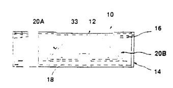
~G~P. 1 is a ~i~9e ~iew of ~ sin~!e le~d pair version o~
t!~e elec~. ic~l conne~~a; cc~r 'ing to t.~e
present :!~vent 1c~n .
~IGURE 2 is ~ lor.gi~udinal sec~ ~ onal ~n~lrged vie~ of the
connec~o~ shown in -IG~R.E 1 with an electric~l
lcad inse~;ed n either end, one of the leads
~ulled to Lhe .se~ cond i ~ ion.
FIG~RE 3 ~ 5 a pP:soec ive view ^' tne ~-clip ins .alled i:
the housin~ of ~he connects~ of FI~URES 1 and ~.
~IGURE 4 is ~ perspective v~ew of ~ douoie lea~ pair
ver~ion of the ocnnec~r ~ccor~ing to the
present inve.~tion wi~.q connec~d detonating C3p
and detonating machine.
FIGURE c io a pl~n sectional view o: the doubl~ lead pdir
version of the connec'or S~own in ~IGUR~ 4 w-th
c~nnect~d detonatins C3~ ~nd detonating machine.
FlGURE 6 is a lenqthwise sectiona' ~iew tnrough the
connector shown in PIGV~E~ 4 and ~,
FIGURE ~ is ~ trar.sverse sectiona; view through t~e
conne~'or shown in FIGUREg ~ a.~d 5.
FICURE 8 is a perspective view of ~he double clip and
delay circuit chip asse~blv incorporate~ i~ the
connectoc shown i n FIGURES 4-6.
. .
2~ 2 1~: 44 ~ 61 i!95GG44 ~ i~ R H~IDGKIN~O~J ~5
208~287
WO9~/lt91- PC~/A~'92/0013
Detailed DescriDtion
..
.q the Follow~ng de ailad desc:.ption, _er~ain specific
r~rminology ~ e e~.ploved for ~:qe sa~e of clari~y and a
par~ l3r emDodi~enr. ~.^, desc-ioed wi~, r -ec?nce to the
drawings. ~lowever, i~ o _e understood that ehe same is
no~ in~ended to be 1i~: ir.C ~nd shou.A no~ be so construed
inas~uo.q ac the nvention .s ca?dble oF takins ~any forms anà
variations wit;qin t;~e sco~e o' the apoe?.d~d ~lai~s,
Refer.ing ~ FIGUR~ e elec~rical connec.or 10 according
t~ ehe ?resen~ i~ven~ion, is adapted ~o elec:ri~ally conne~.
a ~air of eleotric~l 'e3ds SÇC~J~e1~ tocet;qe:, end^to-end,
wi::qou: ehe ~se o~ _.im?i,rg too`~.
The connecto: lC in~ludes ~ housing 1~ defini~g
rectang~larlv sha~ed ineernal cavit~ 14, t:~e housin~
preferably mo1de~ of a suitable rig~d dieiecer.c material,
such AS a Do'yDropylene ?las~ic.
The tqousing 1~ ls elongated and eithe: end receives a pluq
14A, 14~ conf ig~re~ to cl~se off each ~nd thereof secured and
sealed 3t assembly as ~ .sor.ic weldi~g or wit~ a suitable .
adhesive. Each plug 14A, 14~ ~s formed wi~h a pai~ of
c~nlcally tape~ed round boces 1~A, 16B, eac~ adapted to
cecei~e th~ end of a res?ect1~Je electrica' lead A,8. Each
bore 16A, 169 is located of~se~ vertically fro~ the cente! to
be locDted opposi~e the uoper wall of the housing cavity 1l.
~he conneCtor housing ca~it~ 1~ receives a C-clip assem~ly 18
sized to be slldably fit i~t~ the cec~hngul~rly shaped cavi.y ,'
14 ~or~ed ther~ln. ;<
fl
c-cliD 18 defines a oaic o' ter~inal mea~3 f~c sele~ive
connection to ~lectr cal leads, compri~ed of a pair of clip
~6/~ 16: 4~ ~ ~1235~44~ H F liC;DGK l NSl:lN 11~
208~
WO97/1791- PCT~A-'92/0013~
ends 20A, 'OB comDrl~i~c ~..e ~er~inal ~eans, inwa~dly an~l~d
f;om st alqh~ sec~,o-. 2'. ~he en~s 20A, 'QB ~nd straign
section 1 arP cons~-~c~e~ oL d .;o~.~ed .at st:ip Of
electric311v cond~c-ive ~esilie~t :~ateri~l, s~c;q as sD,ir.g
s~el, ~rass, or be~ m ~oope~ he t:-cl~ p ends 20A, 203
a~o inc'ined inwardl~ towacds eacn ot:~er e~ ~rm a ramp
s~rf3ce f~c~ng ~ resoec-;ve ~ui-e noio '5 a~ eit~e~ end.
~he geomet~v o' ~he ^~ ends 2~A, 2~8 is di~ferent from
that disclose~ !n Unite~ St3_es ?2:en- E~ec~ ication ~o
4,952,167, ir. that the ~ps 22.~, 2 9 ~:e bent to decrea~e the
obt~lse ~nql~ and increaee the ac~~e ang!e other-~ise existin9
wi~h cesoec ~C c~n'inin~ surf~ces cf ~ke ~ou3ing 14. ~his
then res~lts i-. a rela~ivel s~ee? ancl~ ~etween ~he tip and
the con~i~inc surfaco o~ ~he ~.ousinc ca~ f 14. ~e C-clip
ends 20A, 20B are de~lected by being asse~bled into the
cavity 14 so that eac~ tip 22A, 229 exert~ some p~essure
against the facing cavity s~rface,
Th~s ~s a lead 24 or 25 is advanced i..to ~he c3vity 14
through a bore 16, it encounte!s the faci~g s~rface o~ the
adjacent C-cliP end 20~, 20B, deflectin~ :he same to enaDle
advancing o{ the lead end between the tl? 2 ~ or 22B of a
respective C-clip 20A, qO~ respect.~e'~ and the surface of
the ho~sing cavity 14,
The i~tended elec~rical connection is e~;~blishe~ oy a
slotted con~act recesses 26A, 26B forme~ ~n the outer edge o~
the respective C-clip ti~ 22~, 2~B,
The width o~ each Of the slotted recosses is ~he ~ame as the
thick~es5 a the lead cond~c~or such as ~~ c~se ~
insulating jacket t~ be sliced through ~s th~ lead 2~, 30 is
p~lled b~ck.
26~ 2 16: 45 2: ~1'`35!,~44~ HCI[~6Kl~J~ûN l ~ l
2~2~
~O 92~1791~ PC~T/AU92/0013
~larious alternate geometries 3rl possible for the cont~ct
recesses 76~, .63, such as ~ s'.ar~ ve2 shaoe geomet:y, or
zo~nded o: ~err3-e.~ ~entral o?eninss inwar~ f.om inc!ined
entry edaes guii ng tne !e~ds ~nto th~ openina. .~ s~r3ns
5ei~ ~rip~ing action between ~n~ t p ~A or ~^3 and the
electrical lead .~ or 3 is est3~ished, causing slicina
~hrough ehe i.~s~lati3n and sea~ ing in the recess 26A or 26B.
'~pon ~ontinued ?ullinc press~.- on t;~ lead ~ or ~, ~he tip
2~ or 273 is p~lled ouewardl~ to en~er a see recess 28~ or
~8a defined a- e` rher er.d c~ '~e connec~or ~J ~ shoulder 30.~,
OB in the up~er surface o t~e ~avity 14, and a con~oured
~nner su~fdce of eac:n of rne ?l~s 14A, 14a. The ~ronq sP1'
grippins eFCeot enab:es each end 20~, ~OB to ~e moved
outw~rdly bv pl~ ling ~occes apD!ied to ~he lead ~ or a to
wedge the same within the i nner su ~ac~s of r~cess 28A, 2~3
with the respective lead A or B.
This setting action anchors the respecti~e ~ lip end 20A,
20~ tO pr~en~ any loosening af ter se~ting of the lead A or
B,
mhe C-cliP assembly ' 3 ~us~ ~e securelv anchored to resist
shif~ing in t~e housing c~vit~ ~ during set~ing of t.~e
leads, and thus ~olded protrusions 32~, 32B, and central
protrus1on 3~ p~ojee:ing ~p from lower hou~ing ~a!l are
rece~ved i~ openings in the ~.r~ight ~ec~ion ~1 for t~is
pll rpo3e .
~n order to insure a waterproof connection, the housinc
ca~ity 11 is ?referably completely filled ~ith a dielectric
gsl ~r g~e3se such as silicone, a s~al1 prooortion oE wh~ch
i~ e~pelled upon inser~ion of a wire, ln5uring continued
complete occlusion of t.hat spacA, and water~roofing
Drotection.
~6/~ 1 ' 92 16: 4~ 1 2Cl'~S44' H ~ ilOD~K INS~I`I 12
~ 20~28'7
WO 92/1,91' PCT~AU9V00}3~
The doub~e lead ~er~lon connector ~ includes a housing 40
su~dl-~ided by a centr3i ~ar~ition ~ ineo a ?air of interna
c~vities 44, ~5, each rect3ncu~ . s:h~?e an~ elonaa~ed so
as to 'ae _a~abl- of ~-ceivi.-s 3 .-soec~iie ~cli~ 48, ;0. A
dou~led ~lug en~ cap S', 5~ :s re~e_~ed :n ~itoer oDen end of
t!~e housln~ ~0, and sonic we' ~ed eo sec~r~ dn~ se~l tne same
t~ the hollsin~ 40.
Ta?ered entL ~nc~ ~oros ~6 are f or;~ed in eac.i plu~ of both end
c~ps 5^, 54 t;~ recei~e an inse-~e- 'ead .~: ~.., 3;, or a4,
dirDcting t.he s~me tO a slot 6~ :n reS~QC~i~e en~ 58~, 58~
59A, 59~ of the ~:-cli3 48 or ~0.
Eac". o- the r-c:i?s ~a and 54 ar~ ~on~lgl:~d sl.nilarlv ~o the
single le~d Dai: ver,;on describe~ ab~v~, excepe that the
resDec~ive ends S8A, ssa and 59A, S9B a.e not di-ectly
el~ctrically co.~neeted, having an interve.r.ing central gap 62
therebe~reen. This ga~ is b~idged by a time delay circuit
chip 64 overlyl~q adjacent ends o4 straight sections 66A, 66
and 57A, 679 assocl~ted with ~-cl~? ends ;~A, 589 ~nd 59A,
59B. The circuit chi? 64 is mec.i~anic311~ and e~ec~ricallv
connected to the straight sec' lOr.S 66A, ~3, and 67A, 673 as
by soldered tabs showr., so as to create a ~n.tar~ assembly
and a time del3y circ~it.
A housing c~ver 70 creates an oDe.ni:lg in t~io top of ~e
housing 40 be~ore assembly, enabl.ng tne ^-~! p and chip
assembl~r to be inst~ll ed in the cavi' ieo ~4, 46, the cover
then 5ealed as by sonic welding.
The p~ition 42 is CUt away to accommodate t!le clip 64, wi~h
a we!~ 72 ntegral wit'n the cover 70 f i' in the gap bet~een
sec~ions of t.'e pa~ ion 42A, ~23 ' o seoa~a~e t.he cavi~ies
4~, 46.
2 1~.: 4 t~ ~ ~. 1 2 ~ 5 ~ t. J i ~ H O C, li K I N S O ~
2~2~7
~(3 ~2/1~91- PCr/Al~'9~/0013C
FI~URE ~ shows -hat 'he .r.vent;cn ma~ t~l~ie ~he form oF a
dou~le 'ead ~alr c~nnec-or 1~ ~Dle to ~nnec each of ~.~e ~wo
!ead pairs .~ ', 31, ~3~ re?ui~ei in ~ach de~on~ion circJit
~etween a fi~ing con;.o. :~nL' '6 3nd ~ ~e~ana ~r 3~.
T~c ch:_ 6~ _~rries ~ su~tab1e ' me delay c r~ie as ~or
example ~e ci~ descri~ed in the above re~erence~ U.~.
patent ~,;.4,18 . some addition~l re~uired e~e~ents SUCrl as
~ oo~e- s~ppl~.~ ca~ac~c~ a ~ e ~o~nted ~o t~e chip 6~ as
described in tne A~ore~entioned ".5. patent. ~he circ~uit on
the chi~ 6~ is de3~ned eo in_roduce a ?rogra~mable delav of
the ti~e of ~rans~is5ion o- a r` r!ng elect. ical c~ ent ?~lse
fro~ a ' ir.no con~r~l ~ani~ ,~ to all ex~lcsi~e de-onator ca~
6~ shown ir. -~5-J~E ~. .; fir:n~ con~-oi ~ 6 :s connec~ ~d
to eaC:~ of ~.~e ex-.)los.~.~e de~ona~^~ de~lces '8 and connectors
34 in a ci~en ~rra~ and controis t.'-e ~.anS~niss.on of
progr3mming and ;ring signals, a'l as desc~ibed in U.S.
Patent No 4,324,182.
Accordin9l~ thc time delay circ~it ma~ be separated f~om ehe
detonator i~sel~ t3 ~a~e man~aac~re easier, and to eli~_na~e
the cons':a~nts i~posed by inCor?oration in~o a pyrotechnic
device de5c ibed acove, a-o well as to ^~via~e 'he need ~or
3tocking ~arietv of detonators.
The inventio- ha5 been descri~ed ~v wav Oc example only wit~.
reference to the delay cir~lit ~e .ng used in association wi'h
detona~or8, but it sho~ld be apoce~iated that the invention
ha~ equal apDlication i~ other areas, s~c:q as domestic,
manu~aceurlng, commercial act:v:t~ss.