Note: Descriptions are shown in the official language in which they were submitted.
- 1 - 20~
1TITLE OF THE INVENTION
SYNCHRONOUS CIRCUIT
BACKGROUND OF THE INVENTION
51. Field of the Invention
The present invention generally relates to
synchronous circuits, and more particularly to a
synchronous circuit in which a frame synchronism is
established using a pointer.
2. Description of the Related Art
A synchronous multiplexing system is widely
employed in the field of digital signal transmission
systems. For example, the CCITT recommends the frame
format shown in Fig. l in an optical digital
transmission-system (see the CCITT Recommendations G.
707, 708 and 709). The frame format shown in Fig. 1 is
used to multiplex pieces of 50Mbps digital data so as
to transfer multiplexed da~a at a bit rate of a few
Gbps. One frame consists of nine rows and has an
overhead 1 and a payload 2. Each of the nine rows has
9N-byte overhead data, and 261N-byte payload data,
wherein N is an arbitrary integer. Supervisory control
information is contained in the overhead l, and
information to be actually transferred, that is, a
virtual container (VC) 3 is contained in the payload 2.
The beginning position of the virtual
container is indicated by pointe~s Hl and H2 included
in the overhead l. The frame format shown in Fig. l is
the format of a frame transferred at a bit rate equal
to N times 155.52 Mbps, and is called an
STM(Synchronous Transport Module)-N. According to the
aforementioned CCITT Recommendations, a plurality of
virtual containers 3 are included in the payload 2 of
the STM-N frame format, and a plurality of pairs of
pointers, such as pointers Hl and H2, are included in
the overhead l of the 5TM-N frame format.
Alternatively, accordlng to the CCITT ~ecommendations,
~ . . , - ,
~ . ': ' . ' ,
'
, .
- 2 - 2~3~
1 one virtual container 3 may be included in the payload
2 of the STM-N frame format, and a pair of pointers may
be included in the overhead 1. The latter frame format
is called concatenation, and the present invention is
concerned with the concatenation frame format.
Fig. 2 is a block diagram of a synchronous
circuit in a digital transmission system. The
synchronous circuit shown in Fig. 2 comprises a frame
synchroni~ing unit 1O1J a frame counter 102, a decoder
10 103, a pointer latch 104, a payload counter 105, a
comparator 106, a VC counter 107, and a zero detector
108. A clock signal shown in (A) of Fig. 3 i5 applied
to the frame synchronizing unit 101, the frame counter
102, the pointer latch 104, the payload counter 105 and
the VC counter 107~
As shown in (B) of Fig. 3, data transferred
in the frame format shown in Fig. 1 is applied to the
frame synchronizing unit 101, which detects a
synchronous pattern contained in the overhead 1. In
(B) of Fig. 3, "SOH" indicates the overhead 1. In
response to the detection of the synchronous pattern,
the frame counter 102 starts to count the number of
bytes in the STM-N ~rame. The decoder 103 decodes the
counter value of the frame counter 102, and generates a
2~ data enable signal shown in (C) of Fig. 3. The data
enable signal causes the payload counter 105 to operate
only while the payload 2 is being received. Further,
the decoder 103 generates a latch timing pulse when the
decoder 103 decodes the counter value indicated by the
pointers Hl and H2. The latch timing pulse generated
by the decoder 103 is applied to the pointer latch 104.
The pointer latch 104 latches the pointers Hl
and H2 contained in the overhead 1 in synchronism with
the latch timing pulse, and outputs them to the
35 comparator 106. The comparator 106 outputs a reset
pulse to the VC counter 107 when the counter value of
the payload counter 105 coincides with the pointer
. .
.~
- 3 -
1 value latched in the pointer latch 104. In response to
receipt of the reset pulse, the zero detector 108
detects a counter value of zero in the VC counter 107,
and generates a frame pulse. As shown in (D) of Fig.
3, the franle pulse indicates the beginning position of
the virtual container VC of the input data. The VC
counter 107 counts the number of bytes included in the
virtual container VC, and is reset every one-~rame
period.
It is requir~ed that the synchronous circuit
operates at higher speeds as the frame bit rate
increases. For example, a high-speed LSI circuit is
required to handle a high-bit-rate signal having a bit
rate of 622.08 Mbps (STM-4) or 2.48832 Gbps (STM-16).
As is well known, compound semiconductor devices, such
as GaAs devices, are capable of operating at speeds
higher than CMOS devices. However, the compound
semiconductor devices need more energy than the CMOS
devices. In a case where the synchronous circuit shown
in Fig. 2 is constructed~using compound semiconductor
devices, it consumes a large amount of energy.
SUMMARY OF THE INVENTION
It is an object of the present invention to
provide a synchronous circuit in which the above
disadvantage is eliminated.
A more specific object of the present
invention is to provide a synchronous circuit that does
not consume a large amount of energy.
The above objects of the present invention
are achieved by a synchronous circuit including a first
block operating in synchronism with a first clock
signal, and a second blocX operating in synchronlsm
with a second clock signal having a frequency lower
than that of the first clock signal. The first block
includes a frame synchronous circuit for detecting a
synchronous pattern contained in input data having a
- ' ' ' , '' ,
~ - .
4 ~ 3~
1 frame format having ~ supervisory control data part and
an information part, the supervisory control data part
including pointer information indicative of a beginning
of the information part. The first block includes a
synchronizing unit for generating, from the synchronous
pattern, a synchronizing control si~nal for
synchronizing the second block operation with the first
block operation. The first block includes a pulse
generator for generating a first frame pulse signal
from the first clock signal and a second frame pulse
signal having a frequency lower than that of the first
frame puIse signal. The second block includes an
information part detecting unit for generating the
second frame pulse signal from the second clock signal
and the synchronizing control signal, the first frame
pulse signal being synchronized with the beginning of
the information part.
BRIEF DESCRIPTION OF THE DRAWINGS
Other objects, features and advantages of the
present invention will become apparent from the
following detailed description when read in conjunction
with the accompanying drawings, in which:
Fig. 1 is a block diagram of a data format
prescribed in the CCITT Recommendations;
- Fig. 2 is a block diagram of a synchronous
circuit;
Fig. 3 is a timing chart showing t~e
operation of the synchronous circuit shown in Fig. 2;
Fig. 4 i5 a block diagram of an overview of a
synchronous circuit of the present invention;
Fig. 5 is a block diagram of a first
embodiment of the~present invention;
Fig. 6 is a diagram showing a frame format of
input data applied to the synchronous circuit shown in
Fig. 4;
Fig. 7 is a block diagram of a pulse
.
. .
-' 2~3~
-- 5 --
1 generator shown in Fig. 6;
Fig. 8 is a timing chart showing the
operation of the pulse generator shown in Fig. 7;
Fig. 9 is a tlming chart showing the
operation of the first embodiment of the present
invention;
Fig. 10 is a block diagram of a second
embodiment of the present invention;
Fig. 11 is a block diagram of a third
embodiment of the present invention; and
Fig. 12 is a block diagram o~ a fourth
embodiment of the present invention.
DESCRIPTION OF THE PREFERRED EMBODIMENTS
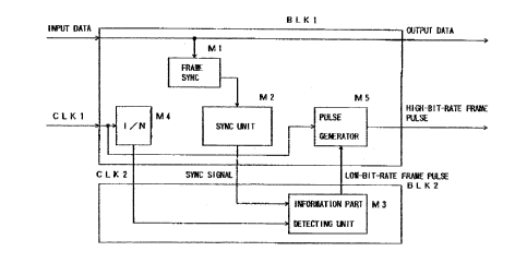
Fig. 4 is a block diagram showing an overview
of the present invention. A synchronous circuit shown
in Fig. l comprises a high-bit-rate circuit block BLKl
serving as a supervisory control data unit, and a low-
bit-rate circuit block BLK2 serving as an information
part unit. The high-bit-rate circuit block BLK1
operates in synchronism with a first clock signal CLKl,
and the low-bit-rate circuit block BLK2 operates in
synchronism with a second clock signal CLK2 having a
frequency equal to l/N times the frequency of the first
clock signal CLKl, wherein N is an integer equal to or
greater than 2.
The high-bit-rate circuit block BLKl is made
up of a frame synchronizing unit Ml, a synchronizing
unit M2, a l/N frequency divider M4, and a pulse
generator M5. The low-bit-rate circuit block BLK2
comprises an information part detecting unit M3. The
frame synchronizing unit M1 detects a synchronous
pattern contained in input data applied to the
high-bit-rate circuit block BLKl. The input data has a
predetermined frame format having an information part
indicated by a pointer contained in the input data.
The synchronous pattern is based on the value indicated
2~18~3~
-- 6 --
1 by the pointer. The synchronizing block M2 generates a
synchronizing control signal that synchronizes the low-
bit-rate circuit block BLE~ with the high-bit-rate
circuit block BLKl in accordance with the synchronous
pattern detected by the frame synchronizing unit Ml.
The synchronizing control signal is applied to the
information part detection unit M3. The l/N frequenCY
divider M4 externally receives the first clock signal
CLKl and generates the second clock signal CLK2 from
the first clock signal CLKl. The second clock signal
CLK2 is applied to the information part detection unit
M3. The first clock signal CLKl is also applied to the
pulse generator M5. The information part detection
unit M3 detects the beginning of the information part
of the input data on the basis of the second clock
signal CLK2 and the synchronizing control signal. The
information part corresponds to, for example, the
virtual container shown in Fig. 1. The information
part detection unit M3 generates a low-bit-rate frame
pulse signal when it detects the beginning of the
information part. The pulse generator M5 receives the
first clock signal CLKl and the low-bit-rate frame
pulse signal, and generates a high-bit rate frame pulse
signal in synchronism with the beginning of the
information part. The high-bit-rate frame pulse signal
has a pulse width less than the period of the first
clock signal CLKl.
Fig. 5 is a block diagram of a synchronous
circuit according to a first embodiment of the present
invention. The synchronous circ~uit shown in Fig. 5
comprises a high-bit-rate circuit block~lOa, and a low-
bit-rate circuit block lOb. The high-bit-rate circuit
block lOa operates in synchronism with the above-
mentioned first clock signal CLKl, and the low-bit-rate
circuit block lOb operates in synchronism~with the
second clock signal CLK2 having a frequency~equal to
l/N times the frequency of the first cloch signal CLKl.
:
, '~
'
.
.
- 7 ~ 3 ~ ~
1 The high-bit-rate circuit block lOa comprise6
a frame synchronous circuit 11, a frame counter 12, a
pointer latch 13, a decoder 14, a payload counter 15, a
comparator 16, a pulse generator 19, and a l/N
frequency divider 20. The low-bit-rate circuit block
lOb comprises a VC counter 17, and a detector 18.
The input data applied to the high-bit-rate
data block lOa is multiplexed digital data, which has a
frame format as shown in Fig. 6. The frame format
shown in Fig. 6 has an overhead 21, and a payload 22
corresponding to the aforementioned information part.
The overhead 21 contains supervisory control dataJ and
the payload 22 contains information to be transmitted.
The frame beginning position of a virtual container
1~ (VC) 23, which is information in $he payload 22 to be
transferred, is indicated by a pointer 24 contained in
the overhead 21. The pointer value of the pointer 24
indicates the ~rame beginning position of the virtual
container 23 of the next frame. The frame format used
in the present invention is, for example, the frame
format prescribed in the CCITT Recommendations G. 707,
708 and 709. According to the above CCITT
Recommendations, the frame format consists of nine
rows, each of which contains 9N-byte overhead data, and
261N-byte payload information. In the format shown in
Fig. 6, one pointer 24 is provided in the overhead 21.
The VC counter 17 indicates the counter value
that changes in synchronism with the second clock
signal CLK2 generated by the l/N frequency divider 20.
More particularly, the VC counter 17 counts the number
of bytes in the virtual container 23, and repeatedlY
changes from "0" to "(9 x 261N - lj". The detector 18
detects the counter value immediately prior to a
counter value of zero, that is, "(9 x 261N -1)", and
3~ generates a low-bit-rate frame pulse signal. The pulse
generator 19 receives the first clock signal CLKl and
the low-bit-rate frame pulse signal, and generates a
:: . ' ' ,.
' . ' ' - .
,
.
~ - 8 - 2 ~8 ~3 ~l~
1 high-bit-rate frame pulse signal having a pulse width
less than the period of the first clock signal CLKl.
Fig. 7 is a block diagram of the pulse
generator 19, which comprises a D-type flip-flop 31, a
latch pulse generator 32, a gate pulse generator 33 and
an AND gate 34. The low-bit-rate frame pulse signal
generated by the detector 18 is applied to a data input
terminal D of the D-type flip-flop 31. The first clock
signal CLKl is applied to the input terminal of the
latch pulse generator 32, which generates a latch pulse
signal applied to a clock terminal CLK of the flip-floP
31.
Fig. 8-(A) shows the first clock signal CLKl,
and Fig. 8-(B) shows the second clock signal CLK2.
Fig. 8-(C) shows the low-bit-rate frame pulse signal
generated by the detector 18, and Fig. 8-~D) shows the
latch pulse signal generated by the latch pulse
generator 32. The pulse width of the low-bit rate
frame pulse signal corresponds to the period of the
second clock signal CLK2.
The first clock signal CLKl is applied to the
gate pulse generator 33, which generates a gate pulse
signal shown in (E) of Fig. 8. The waveform of each
pulse of the gate pulse signal rises in synchronism
with the rise of each pulse of the second clock signal
CLK2, and a pulse width equal to that of the first
clock signal CLKl. The gate pulse signal generated by
the gate pulse generator 33 is applied to the AND gate
34. The output signal of the flip-flop 31 shown in (E)
of Fig. 8 generated via its output terminal Q is
applied to the AND gate 34. The output pulse signal of
the flip-flop 31 is obtained by latching the low-bit-
rate frame pulse in synchronism with the trailing edge
of the latched pulse. The AND gate 34 executes a
logical AND operation on the signals shown in (E) and
(F) of Fig. 8, and generates the high-bit-rate frame
pulse signal shown in (Gj of Fig. 8. The pulse wid$h
, .
, . . .
.~''
. .
- 9 - 2~8~
1 of the high~bit-rate frame signal i~ equal to the pulse
width of the first clock signal CLKl. In this manner,
the high-bit-rate frame signal is generated from the
low-bit-rate frame signal.
The operation of the first embodiment shown
in Fig. 5 will now be described with reference to a
timing chart of Fig. 9. The input data having the
frame format shown in Fig. 6 is applied to the
high-bit-rate circuit block lOa in synchronism with the
first clock signal CLKl. As shown in (A) of Fig. 9,
the first clock signal CLKl is a rectangular wave
signal. Each one byte of the input data is
schematically illustrated in (C) of Fig. 9. The input
data is synchronized with the first clock signal CLKl.
The frame synchronous circuit 11 detects the
synchronous pattern contained in the overhead 21 of the
input data, and outputs a detection signal to the frame
counter 12. In response to receipt of the detection
signal, the frame counter 12 starts to count the number
Of pulses of the first clock signal CLKl. As has been
described previously, the first clock signal CLKl is
synchronized with the period of one byte of the input
data, and hence the counter value of the frame counter
12 indicates the number of bytes in the frame.
The decoder 14 decodes the counter value of
the frame counter 12, and generates a data enable
signal shown in (D) of Fig. 9. The data enable signal
is maintained at a first level during~the period of
transmission of the payload 22 consisting of 261xN
bytes per row, and is maintained at a second level
during the period of transmission of the overhead 21
consisting of 9xN bytes per row. The data enable
signal is applied, as a stop/start control signal, to
the payload counter 15, which is made to operate during
the period of transmission of the payload 22. Further,
the decoder 14 detects the counter value indicating the
position of the pointer 24 included in the overhead 21,
- 10 - 2~ 3~l~
- 1 and outputs the latch timing pulse to the pointer latch
13.
The pointer latch 13 latches the input data
in synchronism with the latch timing pulse signal shown
in (D) of Fig. 8. Hence, the pointer latch 13 holds
the pointer 2~ contained in the overhead 21. The
payload counter 15 is controlled so that it operates
during the period of transmission of the payload 22.
Hence, the counter value of ~he payload counter 15
indicates the number of bytes transmitted during the
period of transmission of the payload 22.
The comparator 15 compares the pointer value
with the counter value of the payload counter 15. When
the values are equal to each other, the comparator 15
outputs a reset pulse signal to the VC counter 17.
After the VC counter 17 is reset, the VC counter 17
starts to count the number of pulses of the second
clock signal CLK2.
At time t1 when the counter value of the VC
counter 17 indicates "(9x261N-1)", the detector 18
generates the low-bit-rate frame signal shown in (E) of
Fig. 9 and (C) of Fig. 8. The low bit-rate frame
signal changes from the high level to the low level at
time t2 one clock pulse after the second clock signal
CLK2 (at this time, the counter value of the VC counter
. 17 becomes zero). Hence, as shown in (F) of Fig. 9 and
(G) o~ Fig. 8, the pulse generator 19 generates the
high-bit-rate frame pulse at time t2 when the counter
value of the VC counter 17 becomes zero. The high-bit-
rate frame pulse has the pulse width equal to the pulse
width of the first clock signal CLK1.
According to the first embodiment of the
present invention, the high-bit-rate operation block
lOa processes data for each byte in synchronism with
the first clock signal CLK1, and the low-bit-rate
operation block lOb, including the VC counter 17 and
the detector 18, operates in synchronism with the
,
.
2~8~3~l~
l second clock signal CLK2 having a frequency e~ual to
l/N times that of the first clock signal CLXl. It will
be noted that the VC counter 17 counts the number of
bytes in the virtual container 23 every predetermined
number of bytes. According to the CCITT
Recommendations, the address value indicated by the
pointers Hl and H2 changes every 4 or 16 bytes (N=4 or
16). Hence, the VC counter 17 counts the number of
bytes in the virtual container 23 every 4 or 16 bytes.
The low-bit-rate operation block lOb does not consume a
large amount oE energy.
A description will now be given of a second
embodiment of the present invention with reference to
Fig. 10, in which parts that are the same as parts
shown in the previously described figures are given the
same reference numbers. A synchronous circuit shown in
Fig. 10 comprises a high-bit-rate operation block 60a,
and a low-bit-rate operation block 60b. The block 60a
comprises the frame synchronous circuit 11, the frame
counter 12, the pointer latch 13, the pulse generator
19 and the l/N frequency divider 20. It should be
noted that the payload counter 15 and the comparator 16
shown in Fig. 5 are not provided in the high-bit rate
operation block 60a.
The low-bit-rate operatio~ block 60b
comprises a payload counter 15', a comparator 16', the
VC counter 17 and the detector 18. The payload counter
15' counts the number of pulses of the second clock
signal CLK2 during only the period of transmission of
the payload 22. The comparator 16' compares the
counter value of the payload counter 15' with the
pointer value latched in the pointer latch 13. When
the difference between the above values becomes equal
to a predetermined value (that is, when the counter
value of the payload counter 15' is substantially equal
to the pointer value in the pointer latch 13~, the
comparator 16' outputs the reset pulse signal to the VC
- 12 - 2~
1 counter 17.
According to the second embodiment of the
present invention, the payload counter 15' and the
comparator 16' operate at the low bit rate in addition
to the VC counter 17 and the detector 18. The payload
counter 15' counts the number of bytes every
predetermined number of bytes based on the frequencY of
the second clock signal CLK2. Hence, the synchronous
circuit shown in Fig. 10 consumes less energy than the
synchronous circuit shown in Fig. S.
Fig. 11 is a block diagram of a third
embodiment of the present invention. In Fig. 11, parts
that are the same as parts shown in the previously
described figures are given the same reference numbers
as previously. A synchronous circuit shown in Fig. 11
comprises a high-bit-rate operation block 70a operating
in synchronism with the first clock signal CLKl, and a
low-bit rate operation block 70b operating in
synchronism with the second clock signal CLK2. The
high-bit-rate operation block 70a comprises a pulse
generator 71 and a pulse generator 72 in addition to
the frame synchronous circuit 11, the pointer latch 13,
the pulse generator l9, and the l/N frequency divider
20. The low-bit-rate operation block 70b comprises a
frame counter 12' and a decoder 14' in addition to the
payload counter 15', the comparator 16', the VC counter
17 and the detector 18.
The frame counter 12' counts the number of
pulses of the second clock CLK2. The decoder 14'
decodes the counter value of the frame counter 12', and
outputs a latch timing signal to the pulse generator 71
provided in the high-bit-rate operation block 70a.
Further, the decoder 14' outputs a stop/start control
signal to the payload counter 15' and the pulse
generator 72. The pulse generators 71 and;72 are
configured in the same manner as the pulse generator
19, and respectively generate, in synchronism with the
- 13 - 2~
1 respective input pulse signals, pulse gignals having a
pulse width less than that of the first clock signal
CLK1. The pulse signal output by the pulse generator
71 is applied, as a latc~ timing signal, to the pointer
latch 13. The pulse signal output by the pulse
generator 72 is applied, as a data enable signal, to &
circuit (not shown) of the next stage.
The frame counter 12' counts the number of
bytes every predetermined number of bytes based on the
frequency of the second clock signal CLK2. The pointer
latch 13 operates every byte, and hence the pulse
generator 71 converts the pulse width of the output
signal of the decoder 14' into a pulse width equal to
that of the first clock signal CLE1. The synchronous
circuit shown in Fig. 11 consumes less energy than the
synchronous circuit shown in Fig. 10.
Fig. 12 is a block diagram of a fourth
embodiment of the present invention. A synchronous
circuit shown in Fig. 12 comprises a high-bit-rate
operation block 80a, and a low-bit-rate operation block
80b. The high-bit-rate operation block 80a comprises a
latch 81 in addition to the frame synchronous circuit
11, the pulse generator 19, the 1/N frequency divider
20 and the pulse generator 72. The low-bit-rate
operation block 80b comprises a pointer latch 13' in
addition to the confi-guration of the block 70b shown in
Fig. 11.
The pointer address value is indicated by the
pointers H1 and H2, which are spaced apart from each
other by a predetermined number of bytes. Hence, the
latch 81 latches the input data in synchronism with the
second clock signal CLK2 generated by the 1/N frequencY
divider 20, and the pointer latch 13' latches the input
data in synchronism with the latch timing signal
generated by the decoder 14'. The synchronous circuit
shown in Fig. 12 consumes less energy than the
synchronous circuit shown in Fig. 11.
- 14 - 2~8~3~
1 The data enable signal and the frame pulse
signal generated by the synchronous circuit of the
present invention are applied to a circuit of the next
stage. For example, the circuit of the next-stage
separates sub-channels contained in the virtual
container 23.
The present invention is not limited to the
specifically disclosed embodiments, and variations and
modifications may be made without departing from the
scope of the present invention.