Note: Descriptions are shown in the official language in which they were submitted.
2n~y~ it
- 1/2 -
LASER ABLATED NOZZLE MEMBER FOR
INKJET PRINTHEAD
FIELD OF THE INVENTION
The present invention generally relates to inkjet
printers and, more particularly, to nozzle or orifice
members and other components for the print cartridges
used in inkjet printers.
BACKGROUND OF THE INVENTION
Thermal inkjet print cartridges operate by rapidly
heating a small volume of ink, causing the ink to
vaporize and be ejected through an orifice to strike a
recording medium, such as a sheet of paper. When a
number of orifices are arranged in a pattern, the
properly sequenced ejection of ink from each orifice
causes characters or other images to be printed upon the
paper as the printhead is moved relative to the paper.
The paper is typically shifted each time the printhead
has moved across the paper. The thermal inkjet printer
is fast and quiet, as only the ink strikes the paper.
These printers produce high quality printing and can be
made both compact and portable.
HP 187337A
._
In one design, the printhead includes: 1) an ink
reservoir and ink channels to supply the ink to the point
of vaporization proximate to an orifice; 2) an orifice
plate in which the individual orifices are formed in the
required pattern; and 3) a series of thin film heaters,
one below each orifice, formed on a substrate which forms
one wall of the ink channels. Each heater includes a thin
film resistor and appropriate current leads. To print a
single dot of ink, an electrical current from an external
power supply is passed through a selected heater. The
heater is ohmically heated, in turn superheating a thin
layer of the adjacent ink, resulting in explosive
vaporization and, consequently, causing a droplet of ink
to be ejected through an associated orifice onto the
paper.
One prior print cartridge is disclosed in United
States Patent 4,500,895 to Buck et al., entitled
"Disposable Inkjet Head," issued February 19, 1985 and
assigned to the present assignee.
In these printers, print quality depends upon the
physical characteristics of the orifices in a printhead
incorporated on a print cartridge. For example, the
geometry of the orifices in a printhead affects the size,
trajectory, and speed of ink drop ejection. In addition,
the geometry of the orifices in a printhead can affect the
flow of ink supplied to vaporization chambers and, in some
instances, can affect the manner in which ink is ejected
from adjacent orifices. Orifice plates for inkjet
printheads often are formed of nickel and are fabricated
by lithographic electroforming processes. One example of
a suitable lithographic electroforming process is
described in United States Patent 4,773,971, entitled
"Thin Film Mandrel" and issued to Lam et al. on September
27, 1988. In such processes, the orifices in an orifice
~: ~,?vt~ 1949v Pv001. BDO
X20305 (BDO:mwI
HP 187337A
- 4 -
plate are formed by overplating nickel around dielectric
discs.
Such electroforming processes for forming orifice
plates for inkjet printheads have several shortcomings.
One shortcoming is that the processes require delicate
balancing of parameters such as stress and plating
thicknesses, disc diameters, and overplating ratios.
Another shortcoming is that such electroforming processes
inherently limit design choices for nozzle shapes and
sizes.
When using electroformed orifice plates and other
components in printheads for inkjet printers, corrosion by
the ink can be a problem. Generally speaking, corrosion
resistance of such orifice plates depends upon two
parameters: ink chemistry and the formation of a hydrated
oxide layer on the electroplated nickel surface of an
orifice plate. Without a hydrated oxide layer, nickel may
corrode in the presence of inks, particularly water-based
inks such as are commonly used in inkjet printers.
Although corrosion of orifice plates can be minimized by
coating the plates with gold, such plating is costly.
Yet another shortcoming of electroformed orifice
plates for inkjet printheads is that the completed
printheads have a tendency to delaminate during use.
Usually, delamination begins with the formation of small
gaps between an orifice plate and its substrate, often
caused by differences in thermal expansion coefficients of
an orifice plate and its substrate. Delamination can be
exacerbated by ink interaction with printhead materials.
For instance, the materials in an inkjet printhead may
swell after prolonged exposure to water-based inks,
thereby changing the shape of the printhead internal
structure.
Even partial delamination of an orifice plate can
result in distorted printing. For example, partial
L: '.M\ 1949\P\001 . BDO
?0305 BDO:mw~
~iP 18'33"A
-
delamination of an orifice plate usually causes decreased
or highly irregular ink drop ejection velocities. Also,
partial delamination can create accumulation sites for air
bubbles that interfere with ink drop ejection.
SUMMARY OF THE INVENTION
A novel nozzle member for an inkjet print cartridge
and method of forming the nozzle member are disclosed. In
a preferred method, the nozzles or orifices are formed by
Excimer laser ablation.
In other aspects of the invention, the vaporization
chambers as well as the ink channels are likewise formed
by Excimer laser ablation.
A frequency multiplied YAG laser may also be used in
place of the Excimer laser.
In one of the preferred embodiments, an inkjet
printhead includes a nozzle member formed of a polymer
material that has been laser-ablated to form inkjet
orifices prior to the nozzle member being mounted to a
substrate. The substrate contains heater elements
associated with each orifice. The polymer material is in
the form of a flexible tape.
The polymer tape preferably is plastic such as
teflon, polyimide, polymethylmethacrylate, polycarbonate,
polyester, polyamide, polyethyleneterephthalate or
mixtures and combinations thereof.
In one particular embodiment of the present
invention, the orifices in the nozzle :ember each have a
barrel aspect ratio (i.e., the ratio of orifice diameter
to orifice length) less than about one-to-one. One
advantage of decreasing the barrel aspect ratio or,
equivalently, extending the barrel length of an orifice
relative to its diameter, is that the positioning of the
orifice and resistor respect ~o a vaporization chamber is
less critical. Another advantage of decreasing the barrel
~:'.Ivf~1949vP001.BDO
920305 BDO:my
CA 02084390 2002-04-02
- 6 -
aspect ratio is that orifices with smaller barrel aspect
ratios have less tendency to entrap air bubbles within
the vaporization chambers.
In a further particular embodiment of the present
invention, heater resistors are mounted directly to a
laser-ablated nozzle member within a vaporization
chamber.
For supplying electrical signals to the heater
resistors, whether mounted on the nozzle member or on a
substrate, the polymer tape is provided with conductive
traces formed thereon using conventional photolitho-
graphic processes.
In accordance with one aspect of the present
invention there is provided an apparatus for use in an
inkjet printer, comprising:
a nozzle member formed in a flexible polymer tape,
said nozzle member having a top surface for facing a
recording medium for printing, said nozzle member having
a plurality of ink orifices formed therein, said orifices
being tapered so as to have an ink exit diameter smaller
than an ink entrance diameter, said orifices being formed
using a laser ablation process prior to said nozzle
member being affixed to a printhead, wherein said
flexible tape containing said nozzle member is cut from a
strip of flexible tape containing a plurality of
identical nozzle members formed using a step-and-repeat
sequence of said laser ablation process.
In accordance with another aspect of the present
invention there is provided a process for forming a
nozzle member for an inkjet printhead, comprising the
steps of
CA 02084390 2002-04-02
- 6a -
forming a nozzle member having a plurality of ink
orifices in a flexible tape using a step-and-repeat laser
ablation process so as to form a repeated sequence of
nozzle members in said flexible tape, each nozzle member
to be subsequently incorporated into a different
printhead;
mounting a plurality of substrates on the flexible
tape to be respectively align with the nozzle members;
and
separating a portion of tape containing a single
nozzle member and a single substrate for use in a single
printhead.
BRIEF DESCRIPTION OF THE DRAWINGS
The present invention can be further understood by
reference to the following description and attached
drawings which illustrate the preferred embodiments.
Other features and advantages will be apparent from
the following detailed description of the preferred
embodiments, taken in conjunction with the accompanying
drawings; which illustrate, by way of example, the
principles of the invention.
Fig. 1 is a perspective view of an inkjet print
cartridge incorporating a printhead in accordance with
one embodiment of the present invention.
Fig. 2 is a perspective view of the front surface of
the Tape Automated Bonding (TAB) printhead assembly
(hereinafter called "TAB head assembly") removed from the
print cartridge of Fig. 1.
Fig: 3 is a perspective view of the back surface of
the TAB head assembly of Fig. 2 with a silicon substrate
mounted thereon and the conductive leads attached to the
substrate.
CA 02084390 2002-04-02
- 6b -
Fig. 4 is a side elevational view in cross-section
taken along line A-A in Fig. 3 illustrating the
attachment
n'P 187337A
of conductive leads to electrodes on the silicon
substrate.
Fig. 5 is a schematic cross-sectional view taken
along line B-B of Fig. 1 showing the seal between the TAB
head assembly and the print cartridge as well as the ink
flow path around the edges of the substrate.
Fig. 6 is a top plan view, in perspective, of a
substrate structure containing heater resistors, ink
channels, and vaporization chambers, which is mounted on
the back of the TAB head assembly of Fig. 2.
Fig. 7 is a top plan view, in perspective, partially
cut away, of a portion of the TAB head assembly showing
the relationship of an orifice with respect to a
vaporization chamber, a heater resistor, and an edge of
the substrate.
Fig. 8 is a side elevational view, in cross-section
and partially cut away, taken along line D-D of Fig. 7 of
the ink ejection chamber of Fig. ,.
Fig. 9 is a side elevational view, in cross-section
and partially cut away, of an ink ejection chamber where a
heater element is located on the nozzle member.
Fig. 10 is a side elevational view, in cross-section
and partially cut away, taken along line E-E of Fig. '~1 of
an ink ejection chamber formed in the tape of Fig. 11
where the nozzle member itself includes ink channels and
vaporization chambers. (The substrate is not shown in
Fig. 11 for clarity.)
Fig. 11 is a perspective view of ''he back surface of
an embodiment of the TAB head assembly where the back
surface of the tape has ink channels and vaporization
chambers formed therein.
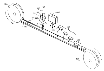
Fig. 12 illustrates one process which may be used to
form any of the TAB head assemblies described herein.
L:'.M11949\P1001. BDO
9'10305 (BDO:mm
HP 187337A
- a -
DETAILED DESCRIPTION OF THE PREFERRED EMBODIMENTS
Referring to Fig. 1, reference numeral 10 generally
indicates an inkjet print cartridge incorporating a
printhead according to one embodiment of the present
invention. The inkjet print cartridge 10 includes an ink
reservoir 12 and a printhead 14, where the printhead 14 is
formed using Tape Automated Bonding (TAB). The printhead
14 (hereinafter "TAB head assembly 14") includes a nozzle
member 16 comprising two parallel columns of offset holes
or orifices 17 formed in a flexible polymer tape 18 by,
for example, laser ablation. The tape 18 may be purchased
commercially as Rapton"' tape, available from 3M
Corporation. Other suitable tape may be formed of Upilex~'
or its equivalent.
A back surface of the tape 18 includes conductive
traces 36 (shown in Fig. 3) formed thereon using a
conventional photolithographic etching and/or plating
process. These conductive traces are terminated by large
contact pads 20 designed to interconnect with a printer.
The print cartridge 10 is designed to be installed in a
printer so that the contact pads 20, on the front surface
of the tape 18, contact printer electrodes providing
externally generated energization signals to the
printhead.
In the various embodiments shown, the traces are
formed on the back surface of the tape 18 (opposite the
surface which faces the recording medium). To access
these traces from the front surface of the tape 18, holes
(vias) must be formed through the front surface of the
tape 18 to expose the ends of the traces. The exposed
ends of the traces are then plated with, for example, gold
to form the contact pads 20 shown cn the front surface of
the tape 18.
Windows 22 and 24 extend through the tape 18 and are
used to facilitate bonding of the other ends of the
L: '.1N\ 1949\P\001. BDO
920305 fBDO:mW
?P 187337A
_ g _
conductive traces to electrodes on a silicon substrate
containing heater resistors. '='he windows 22 and 24 are
filled with an encapsulant to protect any underlying
portion of the traces and substrate.
In the print cartridge 10 of Fig. 1, the tape 18 is
bent over the back edge of the print cartridge "snout" and
extends approximately one half the length of the back wall
25 of the snout. This flap portion of the tape 18 is
needed for the routing of conductive traces which are
connected to the substrate electrodes through the far end
window 22.
Fig. 2 shows a front view of the TAB head assembly 14
of Fig. 1 removed from the print cartridge 10 and prior to
windows 22 and 24 in the TAB head assembly 14 being filled
with an encapsulant.
Affixed to the back of the TAB head assembly 14 is a
silicon substrate 28 (shown in Fig. 3) containing a
plurality of individually energizable thin film resistors.
Each resistor is located generally behind a single orifice
17 and acts as an ohmic heater when selectively energized
by one or more pulses applied sequentially or
simultaneously to one or more of the contact pads 20.
The orifices 17 and conductive traces may be of any
size, number, and pattern, and ~he various figures are
designed to simply and clearly show the features of the
invention. The relative dimensions of the various
features have been greatly adjusted for the sake of
clarity.
The orifice pattern on the tape 18 shown in Fict.
may be formed by a masking process in combination with a
laser or other etching means in a step-and-repeat process,
which would be readily understood by one of ordinary
skilled in the art after reading this disclosure.
Fig. 12, to be described in detail later, provides
additional detail of this process.
.~: '.'N\ I 949\ P.001. HDO
x'10305 BDO:mw~
' ~ 187337A
- 10 -
Fig. 3 shows a back surface of the TAB head assembly
14 of Fig. 2 showing the silicon die or substrate 28
mounted to the back of the tape 18 and also showing one
edge of a barrier layer 30 formed on the substrate 28
containing ink channels and vaporization chambers. Fig. 6
shows greater detail of this barrier layer 30 and will be
discussed later. Shown along the edge of the barrier
layer 30 are the entrances of the ink channels 32 which
receive ink from the ink reservoir 12 (Fig. 1).
The conductive traces 36 formed on the back of the
tape 18 are also shown in Fig. 3, where the traces 36
terminate in contact pads 20 (Fig. 2) on the opposite side
of the tape 18.
The windows 22 and 24 allow access to the ends of the
traces 36 and the substrate electrodes from the other side
of the tape 18 to facilitate bonding.
Fig. 4 shows a side view cross-section taken along
line A-A in Fig. 3 illustrating the connection of the ends
of the conductive traces 36 to the electrodes 4o formed on
the substrate 28. As seen in Fig. 4, a portion 42 of the
barrier layer 30 is used to insulate the ends of the
conductive traces 36 from the substrate 28.
Also shown in Fig. 4 is a side ~niew of the tape 18,
the barrier layer 30, the windows ~2 and 24, and the
entrances of the various ink channels ~2. Droplets 46 of _
ink are shown being ejected from orifice holes associated
with each of the ink channels 32.
The back surface of the TAB assembly 14 in Fig. 3 is
sealed, as shown in Fig. 5, with respect to an ink opening
in the ink reservoir 12 by an adhesive seal which
circumscribes the substrate 28 and for:~s an ink seal
between the back surface of the tape '~3 and the ink
reservoir 12.
Shown in Fig. 5 is a side elevational view in cross-
section taken along line B-B in Fig. ~ showing a portion
~: '.!H~ 1949\P 001. BDO
~?0305 lH DO: mm
hP 187337A
- 11 -
of the adhesive seal 50 surrounding the substrate 28 and
showing the substrate 28 being adhesively secured to a
central portion of the tape 18 by a thin adhesive layer 52
on the top surface of the barrier layer 30 containing the
ink channels and vaporization chambers 54 and 56. A
portion of the plastic body of the printhead cartridge 10
is also shown. Thin film resistors 58 and 60 are shown
within the vaporization chambers 54 and 56, respectively.
Fig. 5 also illustrates how ink 62 from the ink
reservoir 12 flows through the central slot 64 formed in
the print cartridge 10 and flows around the edges of the
substrate 28 into the vaporization chambers 54 and 56.
When the resistors 58 and 60 are energized, a portion of
the ink within the vaporization chambers 54 and 56 is
ejected, as illustrated by the emitted drops of ink 66
and 68.
Fig. 6 is a front top plan view, in perspective, of
the silicon substrate 28 which is affixed to the back of
the tape 18 in Fig. 2 to form the TAH head assembly 14.
Silicon substrate 28 has formed on it, using
conventional photolithographic techniques, two rows of
thin film resistors 70, shown in Fig. 6 exposed through
the vaporization chambers 72 formed in the barrier
layer 30.
In one embodiment, the substrate 23 is approximately
one-half inch long and contains 300 heater resistors 70,
thus enabling a resolution of 600 dots per inch.
Also formed on the substrate 28 are electrodes 74 for
connection to the conductive traces 36 (shown by dashed
lines) formed on the back of the tape 18 in Fig. 2.
A demultiplexer 78, shown by a dashed outline in
Fig. 6, is also formed on the substrate c8 for
demultiplexing the incoming multiplexed signals applied ~o
the electrodes 74 and distributing the signals to the
various thin film resistors 70. The demultiplexer 78
L:'.M\ 1949\ P\001. BDO
?0305 (BDO:my
i~ 187337A
- i2 -
enables the use of much fewer electrodes 74 than thin film
resistors 70. The demultiplexer 78 may be any decoder For
decoding encoded signals applied to the electrodes 74.
Also formed on the surface of the substrate 28 using
conventional photolithographic techniques is the barrier
layer 30, which may be a layer of photoresist or some
other polymer, in which is formed the vaporization
chambers 72 and ink channels 80.
A portion 42 of the barrier layer 30 insulates the
conductive traces 36 from the underlying substrate 28, as
previously discussed with respect to Fig. 4.
In order to adhesively affix the top surface of the
barrier layer 30 to the back surface of the tape 18 shown
in Fig. 3, a thin adhesive layer 84, such as an uncured
layer of photoresist, is applied to the top surface of the
barrier layer 30. A separate adhesive layer may not be
necessary if the top of the barrier layer 30 can be
otherwise made adhesive. The resulting substrate
structure is then positioned with respect to the back
surface of the tape 18 so as to align the resistors 70
with the orifices formed in the tape 18. This alignment
step also inherently aligns the electrodes 74 with the
ends of the conductive traces ~6. The traces 36 are then
bonded to the electrodes i4. This alignment and bonding
process is described in more detail later with respect to
Fig. 12. The aligned and bonded substrate/tape structure
is then heated while applying pressure to cure the
adhesive layer 84 and firmly affix the substrate structure
to the back surface of the tape 18.
Fig. 7 is an enlarged view of a single vaporization
chamber 72, thin film resistor ;0, and orifice 17 after
the substrate structure of Fig. 5 is secured to the back
of the tape 18 via the thin adhesive layer 84. A side
edge of the substrate 28 is shown as edge 86. ~n
operation, ink flows from the ink reservoir 12 in Fig. ?,
L:',IH~ 1949v Pv001. 8 DO
920305 lH DO: mw 1
- i3 -
:3P 187337A
around the side edge 86 of the substrate 28, and into the
ink channel 80 and associated vaporization chamber 72, as
shown by the arrow 88. Upon energization of the thin film
resistor 70, a thin layer of the adjacent ink is
superheated, causing explosive vaporization and,
consequently, causing a droplet of ink to be ejected
through the orifice 17. The vaporization chamber 72 is
then refilled by capillary action.
In a preferred embodiment, the barrier layer 30 is
approximately 1 mils thick, the substrate 28 is
approximately 20 mils thick, and the tape 18 is
approximately 2 mils thick.
Fig. 8 is a side elevational view in cross-section
taken along line C-C in Fig. 1 of one ink ejection chamber
in the TAB head assembly 14 in accordance with one
embodiment of the invention. The cross-section shows a
laser-ablated polymer nozzle member 90 laminated to a
barrier layer 30, which may be similar to that shown in
Fig. 6. When the thin film resistor 70 on the substrate
28 is energized, a portion of the ink within the
vaporization chamber 72 is vaporized, and an ink droplet
91 is expelled through the orifice 17.
Fig. 9 is a side elevational view in cross-section of
an alternative embodiment of an ink ejection chamber using
a polymer, laser-ablated nozzle member 92. As in the
above-described embodiments, a vaporization chamber 72 is
bounded by the nozzle member 92, the substrate 28, and the
barrier layer 30. In contrast to the above-described
embodiments, however, a heater resistor 94 is mounted on
the undersurface of the nozzle member 92, not on the
substrate 28. This enables a simpler construction of the
printhead.
Conductive traces (such as shown in Fig. 3) formed on
the bottom surface of the nozzle member 92 provide
electrical signals to the resistors 94.
..: '.M~ 1949~P.pp1 . BDO
X20305 fBDO:mW
~iP 187337A
- 1 ,~ -
The various vaporization chambers discussed herein
can also be formed by laser-ablation in a manner similar
to forming the nozzle member. More particularly,
vaporization chambers of selected configurations can be
formed by placing a lithographic mask over a layer of
polymer, such as a polymer tape, and then laser-ablating
the polymer layer with the laser light in areas that are
unprotected by the lithographic mask. In practice, the
polymer layer containing the vaporization chambers can be
bonded to, be formed adjacent to, or be a unitary part of
a nozzle member.
Fig. 10 is a side elevational view in cross-section
of a nozzle member 96 having orifices, ink channels, and
vaporization chambers 98 laser-ablated in a same polymer
layer. The formation of vaporization chambers by laser
ablation as a unitary part of a nozzle member, as shown in
Fig. 10, is greatly assisted by the property of laser
ablation of forming a recessed chamber with a
substantially flat bottom, provided the optical energy
density of the incident laser beam is constant across the
region being ablated. The depth of such chambers is
determined by the number of laser shots, and the energy
density of each.
If the resistor, such as the resistor 70 in Fig. 10,
is formed on the nozzle member 96 itself, the substrate 28
may be eliminated altogether.
Fig. 11 shows the back surface of the nozzle member
96 in Fig. 10 prior to a substrate being affixed thereon.
The vaporization chambers 98, ink channels 99, and ink
manifolds 100 are formed part :.gay through the thickness of
the nozzle member 96, while orifices, such as the orifices
17 shown in Fig. 2, are formed completely through the
thickness of the nozzle member 96. Ink from an ink
reservoir flows around the sides cf a substrate (not
shown) mounted on the back surface of the nozzle member
L:'.t~n1949vP\OOI .BDO
°?0305 ~BDO:mW
HP 18733'A
.r
96, then into the ink manifolds 100, and then into the ink
channels 99 and vaporization chambers 98. The windows 22
and 24, used for bonding as previously discussed, are also
shown.
Multiple lithographic masks may be used to form the
orifice and ink path patterns in the unitary nozzle
member 96.
Fig. 12 illustrates a method for forming either the
embodiment of the TAB head assembly 14 in Fig. 3 or the
TAB head assembly formed using the nozzle member 96 in
Fig . 11.
The starting material is a Kapton~' or Upilex'~-type
polymer tape 104, although the tape 104 can be any
suitable polymer film which is acceptable for use in the
below-described procedure. Some such films may comprise
teflon, polyimide, polymethylmethacrylate, polycarbonate,
polyester, polyamide, polyethylene-terephthalate or
mixtures thereof.
The tape 104 is typically produced in long strips on
a reel 105. Sprocket holes 106 along the sides of the
tape 104 are used to accurately and securely transport the
tape 104. Alternately, the sprocket holes 106 may be
omitted and the tape :gay 'a tr ansported with other ~-ypes
of fixtures.
In the preferred embodiment, the tape 104 is already
provided with conductive copper traces 36, such as shown
in Fig. 3, formed thereon using conventional photo-
lithographic and metal deposition processes. The
particular pattern of conductive traces depends on the
manner in which it is desired to distribute electrical
signals to the electrodes forzled on silicon dies, which
are subsequently mounted on the tape 104.
In the preferred process, the tape 104 is transported
to a laser processing chamber and laser-ablated in a
pattern defined by one or :yore :asks 108 using laser
~:.M\I949\p\OOI.BDO
920305 BDO:mW
m a i 337A
- '~ 5 -
radiation 110, such as that generated by an Excimer laser
112 of the Fz, ArF, KrCl, KrF, or XeCl type. The masked
laser radiation is designated by arrows 114.
In a preferred embodiment, such masks 108 define all
of the ablated features for an extended area of the tape
104, for example encompassing multiple orifices in the
case of an orifice pattern mask 108, and multiple
vaporization chambers in the case of a vaporization
chamber pattern mask 108. Alternatively, patterns such as
the orifice pattern, the vaporization chamber pattern, or
other patterns may be placed side by side on a common mask
substrate which is substantially larger than the laser
beam. Then such patterns may be moved sequentially into
the beam. The masking material used in such masks will
preferably be highly reflecting at the laser wavelength,
consisting of, for example, a multilayer dielectric or a
metal such as aluminum.
The orifice pattern defined by the one or more masks
108 may be that generally shown in Fig. 2. Multiple masks
108 may be used to form a stepped orifice taper as shown
in Figs. 8-l0.
In one embodiment, a separate mask 108 defines the
pattern of windows 22 and 24 shown in Figs. 2 and 3;
however, in the preferred embodiment, the windows 22 and
24 are formed using conventional photolithographic methods
prior to the tape 104 being subjected to the processes
shown in Fig. 12.
In the embodiment of Figs. 10 and 11, where the
nozzle member also includes vaporization chambers, one or
more masks 108 would be used to form the orifices and
another mask 108 and laser energy level (and/or number of
laser shots) would be used to define the vaporization
chambers, ink channels, and manifolds which are formed
through a portion of the thickness of the tape 104.
L: ~.IH~ 1949vP1001.BDO
?0305 BDO:mwl
- 17 -
iP 187337A
The laser system for this process generally includes
beam delivery optics, alignment optics, a high precision
and high speed mask shuttle system, and a processing
chamber including a mechanism for handling and positioning
the tape 104. In the preferred embodiment, the laser
system uses a projection mask configuration wherein a
precision lens 115 interposed between the mask 108 and the
tape 104 projects the Excimer laser light onto the tape
104 in the image of the pattern defined on the mask 108.
The masked laser radiation exiting from lens 115 is
represented by arrows 116.
Such a projection mask configuration is advantageous
for high precision orifice dimensions, because the mask is
physically remote from the nozzle member. Soot is
naturally formed and ejected in the ablation process,
traveling distances of about one centimeter from the
nozzle member being ablated. If the mask were in contact
with the nozzle member, or in proximity to it, soot
buildup on the mask would tend to distort ablated features
and reduce their dimensional accuracy. In the preferred
embodiment, the projection lens is more than two
centimeters from the nozzle member being ablated, thereby
avoiding the buildup of any soot on it or on the mask.
Ablation is well known to produce features with
tapered walls, tapered so that the diameter of an orifice
is larger at the surface onto which the laser is incident,
and smaller at the exit surface. The taper angle varies
significantly with variations in the optical energy
density incident on the nozzle member for energy densities
less than about two joules per square centimeter. If the
energy density were uncontrolled, the orifices produced
would vary significantly in taper angle, resulting in
substantial variations in exit orifice diameter. Such
variations would produce deleterious variations in ejected
ink drop volume and velocity, reducing print quality. in
~: '.!N\ 1949\P',001. BDO
°?0305 (HDO:mw1
iP 187337A
- 1
the preferred embodiment, the optical energy of the
ablating laser beam is precisely monitored and controlled
to achieve a consistent taper angle, and thereby a
reproducible exit diameter. In addition to the print
quality benefits resulting from the constant orifice exit
diameter, a taper is beneficial to the operation of the
orifices, since the taper acts to increase the discharge
speed and provide a more focused ejection of ink, as well
as provide other advantages. The taper may be in the
range of 5 to 15 degrees relative to the axis of the
orifice. The preferred embodiment process described
herein allows rapid and precise fabrication without a need
to rock the laser beam relative to the nozzle member. It
produces accurate exit diameters even though the laser
beam is incident on the entrance surface rather than the
exit surface of the nozzle member.
After the step of laser-ablation, the polymer tape
104 is stepped, and the process is repeated. This is
referred to as a step-and-repeat process. The total
2o processing time required for forming a single pattern on
the tape 104 may be on the order of a few seconds. hs
mentioned above, a single mask pattern may encompass an
extended group of ablated features to reduce the
processing time per nozzle member.
Laser ablation processes have distinct advantages
over other forms of laser drilling for the formation of
precision orifices, vaporization chambers, and ink
channels. In laser ablation, short pulses of intense
ultraviolet light are absorbed in a thin surface layer of
material within about 1 micrometer or less of the surface.
Preferred pulse energies are greater than about 100
millijoules per square centimeter and pulse durations are
shorter than about 1 microsecond. Under these conditions,
the intense ultraviolet light photodissociates the
chemical bonds in the material. Furthermore, the absorbed
~:'.hf~1949vP10p1.HD0
°20305 BDO:mw1
ar
CA 02084390 2002-12-05
- 19 -
ultraviolet energy is concentrated in such a small volume
of material that it rapidly heats the dissociated
fragments and ejects them away form the surface of the
material. Because these processes occur so quickly,
there is no time for heat to propagate to the surrounding
material. As a result, the surrounding region is not
melted or otherwise damaged, and the perimeter of ablated
features can replicate the shape of the incident optical
beam with precision on the scale of about one micrometer.
In addition, laser-ablation can also form chambers with
substantially flat bottom surfaces which form a plane
recessed into the layer, provided the optical energy
density is constant across the region being ablated. The
depth of such chambers is determined by the number of
laser shots, and the power density of each.
Laser-ablation processes also have numerous
advantages as compared to conventional lithographic
electroforming processes for forming nozzle members for
inkjet printheads. For example, laser-ablation processes
generally are less expensive and simpler than
conventional lithographic electroforming processes. In
addition, by using laser-ablations processes, polymer
nozzle members can be fabricated in substantially larger
sizes (i.e., having greater surface areas) and with
nozzle geometries that are not practical with
conventional electroforming processes. In particular,
unique nozzle shapes can be produced by controlling
exposure intensity or making multiple exposures with a
laser beam being reoriented between each exposure. Also,
precise nozzle geometries can be formed without
P 18733"A
- 20
process controls as strict as those required for
electroforming processes.
Another advantage of forming nozzle members by laser-
ablating a polymer material is that the orifices or
nozzles can be easily fabricated with ratios of nozzle
length (L) to nozzle diameter (D) greater than
conventional. In the preferred embodiment, the L/D ratio
exceeds unity. One advantage of extending a nozzle s
length relative to its diameter is that orifice-resistor
positioning in a vaporization chamber becomes less
critical.
In use, laser-ablated polymer nozzle members for
inkjet printers have characteristics that are superior to
conventional electroformed orifice plates. For example,
laser-ablated polymer nozzle members are highly resistant
to corrosion by water-based printing inks and are
generally hydrophobic. Further, laser-ablated polymer
nozzle members have a relatively low elastic modulus, so
built-in stress between the nozzle member and an
underlying substrate or barrier layer has less of a
tendency to cause nozzle member-to-barrier layer
delamination. Still further, laser-ablated polymer nozzle
members can be readily fixed to, or formed with, a polymer
substrate.
Although an Excimer laser is used in the preferred
embodiments, other ultraviolet light sources with
substantially the same optical wavelength and energy
density may be used to accomplish the ablation process.
Preferably, the wavelength of such an ultraviolet light
source will lie in the 150 nm to 400 nm range to allow
high absorption in the tape to be ablated. Furtherr~,cre,
the energy density should be greater than about 100
millijoules per square centimeter with a pulse length
shorter than about 1 microsecond to achieve rapid ejection
L:'.M\ 1949\ P\001. HDO
y20305 BDO:mwl
riP 187337A
- 21 -
of ablated material with essentially no heating of the
surrounding remaining material.
As will be understood by those of ordinary skill in
the art, numerous other processes for forming a pattern on
the tape 104 may also be used. Other such processes
include chemical etching, stamping, reactive ion etching,
ion beam milling, and molding or casting on a photodefined
pattern.
A next step in the process is a cleaning step wherein
the laser ablated portion of the tape 104 is positioned
under a cleaning station 117. At the cleaning station
117, debris from the laser ablation is removed according
to standard industry practice.
The tape 104 is then stepped to the next station,
which is an optical alignment station 118 incorporated in
a conventional automatic TAB bonder, such as an inner lead
bonder commercially available from Shinkawa Corporation,
model number IL-20. The bonder is preprogrammed with an
alignment (target) pattern on the nozzle member, created
in the same manner and/or step as used to created the
orifices, and a target pattern on the substrate, created
in the same manner and/or step used to create the
resistors. In the preferred embodiment, the nozzle member
material is semi-transparent so that the target pattern on
the substrate may be viewed through the nozzle member.
The bonder then automatically positions the silicon dies
120 with respect to the nozzle members so as to align the
two target patterns. Such an alignment feature exists in
the Shinkawa TAB bonder. This automatic alignment of the
nozzle member target pattern with the substrate target
pattern not only precisely aligns the orifices with the
resistors but also inherently aligns the electrodes cn the
dies 120 with the ends of the conductive traces formed in
the tape 104, since the traces and the orifices are
aligned in the tape 104, and the substrate electrodes and
L:'.Ivt\ 1449vPv001. BDO
920305 (BDO:my
208~~~
P 187337A
- 22 -
the heating resistors are aligned on the substrate.
Therefore, all patterns on the tape 104 and on the silicon
dies 120 will be aligned with respect to one another once
the two target patterns are aligned.
Thus, the alignment of the silicon dies 120 with
respect to the tape 104 is performed automatically using
only commercially available equipment. By integrating the
conductive traces with the nozzle member, such an
alignment feature is possible. Such integration not only
reduces the assembly cost of the printhead but reduces the
printhead material cost as well.
The automatic TAB bonder then uses a gang bonding
method to press the ends of the conductive traces down
onto the associated substrate electrodes through the
windows formed in the tape 104. The bonder then applies
heat, such as by using thermocompression bonding, to weld
the ends of the traces to the associated electrodes. A
side view of one embodiment of the resulting structure is
shown in Fig. 4. Other types of bonding can also be used,
2o such as ultrasonic bonding, conductive epoxy, solder
paste, or other well-known means.
The tape 104 is then stepped to a heat and pressure
station 122. As previously discussed with respect to
Figs. 6 and 7, an adhesive layer 84 exists on the top
surface of the barrier layer 30 formed on the silicon
substrate. After the above-described bonding step, the
silicon dies 120 are then pressed down against the tape
104, and heat is applied to cure the adhesive layer 84 and
physically bond the dies 120 to the tape 104.
Thereafter the tape 104 steps and is optionally taken
up on the take-up reel 124. The tape 104 may then later
be cut to separate the individual TAB head assemblies from
one another.
The resulting TAB head assembly is then positioned on
the print cartridge 10, and the previously described
L: .Iy(\ 1949\P\001. BDO
920305 BDO:mwl
~0~4~~~
iP 187337A
- 23 -
adhesive seal 50 in Fig. 5 is formed to firmly secure the
nozzle member to the print cartridge, provide an ink-proof
seal around the substrate between the nozzle member and
the ink reservoir, and encapsulate the traces extending
from the substrate so as to isolate the traces from the
ink.
Peripheral points on the flexible TAB head assembly
are then secured to the plastic print cartridge 10 by a
conventional melt-through type bonding process to cause
the polymer tape 18 to remain relatively flush with the
surface of the print cartridge 10, as shown in Fig. 1.
The foregoing has described the principles, preferred
embodiments and modes of operation of the present
invention. However, the invention should not be construed
as being limited to the particular embodiments discussed.
As an example, the above-described inventions can be used
in conjunction with inkjet printers that are not of the
thermal type, as well as inkjet printers that are of the
thermal type. Thus, the above-described embodiments
should be regarded as illustrative rather than
restrictive, and it should be appreciated that variations
may be made in those embodiments by workers skilled in the
art without departing from the scope of the present
invention as defined by the following claims.
L:'.IN~ 1949 P\001. HDO
920305 IHDO:mm