Note: Descriptions are shown in the official language in which they were submitted.
208~394
SPECIFICATION
Titlc of the Invention
SUPERCONDUCIlNG MULTILAYER
S INTERCONNECI ION FORMED OF OXIDE
SUPERCONDUCTOR MATERIAL AND METHOD FOR
MANUFACI'URING THE SAME
Background of the Invention
Field of the invention
The present invention relates to a multilayer interconnection and
method for manufacturing the multilayer interconnection. More
specifically to a multilayer interconnection formed of oxide
super~ d~lctQr material and method for manufacturing the same.
Description of related art
A superconducting current path is one of the electronic applications
of a superconductor. If all the current paths of a conventional electronic
circuit including semiconductor devices is replaced with superconducting
2 0 current paths, completely, the electronic circuit will operate rapidly with
low power consumption. Su~er~ol~d~1ctin~ signal paths are also expected
to reduce the wave form distortion so that the required number of
amplifiers and/or repeaters can be reduced. Particularly, by using an
o~cide superconductor material which has been recently advanced in study,
it is possible to produce a superconducting current path through which
su~o~ cting current flows at relatively high ~..Il.erature.
2Q84~9~
An oxide superconductor has the largest critical current density Jc
in direction perpendicular to c-axes of its crystal }attices. Therefore, it is
desirable that the superconducting current path through which
supcrconducting current flows horizontally is formed of a c-ax~s
S orient~te~ oxide superconductor thin film and the superconducting path~rough which superconducting cu~rent flows vertically is formed of
oxide superconductor thin films of which c-axes are orient~te~
horizontally. In this specification, this oxide superconductor thin film of
which c-axes are orientated horizontally wi31 be called an r'a-axis
ori~n~t~ oxide superconductor thin film".
In a prior art, a superconducting multilayer interconnection which
has layered superconducting current paths constituted of c-axis orientated
oxide s~perconductor thin films and a superconducting interconnect
current path constituted of an a-axis orientated oxide superconductor thin
1 S film is proposed. In the superconducting multilayer interconnection, the
superconducting interconnect current path is formed at a via hole
~n~t~ating through the layered superconducting current paths. The via
ho}e increases the occupied area of the superconducting multilayer
u~t4~col~n~ction.
2 0 In addition, grain boundaries are 8enerated at the interface between
the c-axis orientated oxide superconductor thin fflm and the a-axis
orient~te~ oxide superconductor thin film, which introduce difficulties of
supercond~lctin~ current flowing. The 8rain boundaries sometimes fonn
Josephson junctions which pass only tunnel current so that the current
capability is limited and the input and output characteristics become
nor~ e~r, Even if no Josephson junction is formed at the interface, ~oule
heat may be generated by the electrical resistance formed at the interface,
2n84394
-
which causes the "quench" phenomenon. Furthermore, the c-axis
orientated oxide superconductor thin filrn and the a-axis orientated oxide
superconductor thin film may interfere with each other so as to degrade
each other.
S In order to manufacture the above superconducting multilayer
interconnection, in a prior art, the via hole is formed through layered
superconducting current paths and insulating layers and an a-axis
orientated oxide superconductor thin film is formed in the via hole. The
diameter of the via hole is made small in order to decrease the occupied
area of the superconducting multilayer interconnection. Therefore, the
side surface of the via hole can not be cleaned enough, which generates an
unnecessary Josephson junction when the a-axis orientated oxide
superconductor thin film is formed.
Summary of the Invention
Accordingly, it is an object of the present invention to provide a
superconducting multilayer interconnection of an oxide superconductor,
which addresses the above mentioned defects of the conventional ones.
lf .i~3
,:
2084394
In accordance with the present invention there is
provided a superconducting multilayer intercormection
comprising a substrate having a principal surface, a first
superconducting current path of a c-axis orientated oxide superconductor
S thin film formed on the principal surface of the substrate, an insulating
layer on the first superconducting current path, a second superconducting
current path of a c-axis orientated oxide superconductor thin film formed
on the insulating layer so that the first and second superconducting
current paths are insulated by the insulating layer, and a superconducting
10 interconnect current path of an a-axis orientated oxide superconductor
thin film, through which the first and second superconducting current
paths are electrically connected each other in which at least one of the
first and second superconducting current paths has a step portion and the
superconducting interconnect current path is positioned at the step portion
15 so that the interface area between the superconducting current path and
the superconducting interconnect current path is enlarged.
In the superconducting multilayer interconnection, the interface
between the superconducting current path and the superconducting
interconnect current path is preferably inclined so as to enlarge the
2 0 contact area.
In one preferred embodiment, the substrate has a step on the
principal surface so that the first and second superconducting current path
have step portions on the step of the substrate, and the superconducting
interconnect current path is positioned on the step of the substrate.
25 Namely, the superconducting current paths and insulating layers are
stacked on the principal surface of the substrate having a step so that each
of them also has a step at the step of the substrate.
2084394
In another preferred embodiment, the superconducting interconnect
current path includes an insulating layer formed of an a-axis orientated
PrlBa2Cu307.f oxide thin film.
- In a preferred embodiment, the oxide superconductor is formed of
5 high-TC (high critical temperature) oxide superconductor, particularly,
formed of a high-TC copper-oxide type compound oxide superconductor
for example a Y-Ba-Cu-O compound oxide superconductor material and a
Bi-Sr-Ca-Cu-O compound oxide superconductor material.
In addition, the substrate can be formed of an insulating substrate,
10 preferably an oxide single crystalline substrate such as MgO, SrTiO3,
CdNdA104, etc. These substrate materials are very effective in forming
or growing a crystalline film having a high degree of crystalline
orientation.
A superconducting multilayer interconnection may comprise a
substrate having a principal surface, a first superconducting current path
of a c-axis orientated oxide superconductor thin film formed on the
principal surface of the substrate, an insulating layer on the first
superconducting current path, a second superconducting current path of a
2 0 c-axis orientated oxide superconductor thin film formed on the insulating
layer so that the first and second superconducting current paths are
insulated by the insulating layer, and an interconnect current path through
which the first and second superconducting current paths are electrically
connected each other, which is constituted of two noble metal layers and a
2 5 resistor layer inserted between the noble metal layers.
2084394
In this case, the occupied area of the superconducting multilayer
interconnection can be reduced so that it is desirable to apply it to an
integrated circuit.
A method for manufacturing a superconducting multilayer
interconnection may comprise the steps of forming a seed layer on which an
a-axis orientated oxide superconductor thin film grows under a condition
of growing c-axis orientated oxide superconductor thin film at a portion
of a principal surface of a substrate, on which superconducting
10 interconnect current path will be positioned, forming a first oxide
superconductor thin film under a condition of growing c-axis orientated
oxide superconductor thin film on the principal surface of the substrate so
that an a-axis orientated oxide superconductor thin filrn grows on the seed
layer, processing the first oxide superconductor thin film so as to form a
15 first superconducting current path, depositing an insulating layer on the
first superconducting current path, pattern-etching the insulating layer so
that the a-axis orientated oxide superconductor thin film is exposed and
the first superconducting current path is not exposed, forming a second
oxide superconductor thin film under a condition of growing c-axis
2 0 orientated oxide superconductor thin film on the insulating layer so that
an a-axis orientated oxide superconductor thin film grows on the exposed
a-axis orientated oxide superconductor thin film and processing the
second oxide superconductor thin film so as to form a second
superconducting current path which is electrically connected to the first
25 superconducting current path through a superconducting interconnect
current path formed of the a-axis orientated oxide superconductor thin
films on the seed layer.
- 2084394
The seed layer can be formed of an a-axis orientated oxide
superconductor thin film or an a-axis orientated PrlBa2Cu307 ~ oxide thin
film. An insulating layer can be formed in the superconducting
interconnect current path by using an a-axis orientated PrlBa2cu3o7-e
S oxide thin film.
The above and other objects, features and advantages of the present
invention will be apparent from the following description of preferred
embodiments of the invention with reference to the accompanying
drawings.
1 0
Brief Description of the Drawings
Figures lA to lF are diagrammatic sectional views for illustrating a
method for manufacturing a first embodiment of a superconducting
multilayer interconnection;
Figures 2A to 2I are diagrammatic sectional views for illustrating a
method for manufacturing a second embodiment of the superconducting
multilayer interconnection; and
Figure 3 is a diagrammatic sectional view of a third embodiment of
the superconducting multilayer interconnection.
Description of the Preferred embodiments
Embodiment 1
Referring to Figures lA to lF, a method for manufacturing an
25 embodiment of the the superconducting multilayer interconnection
will be described.
.~
2n8439~
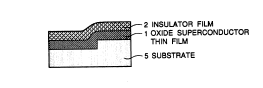
As shown in Figure 1~, an MgO substrate 5 having a step on a
principal surface is prepared. The step can be formed by an etching
process. A superconducting int~rc~nnect current path will be formed at
dle step portion.
As shown in Figure lB, a c-axis orientated YlBa2Cu3O7.~ oxide
supcrconductor thin film 1 is formed on the principal surf~ce of the
substrate S by a sputtering. The c-axis orientated YlBa2Cu307.~ oxide
superconductor thin film 1 is preferably formed by a sputtering,
particularly off-axis sputtering. The condition of fo~ning the c-axis
orientPtell YlBa2Cu3O7.~ oxide superconductor thin film 1 by off-axis
s~lueling is as follows:
Sputtering Gas Ar: 90%
2 1 0%
Total pressure S x 10-2 Torr
Tenl~erature of the substr~te 700DC
The c-axis orientated YIBa2Cu3(;~7 ~ oxide superconductor thin
film 1 will constitute a superconducting current path through which
superconducting current will flow in parallel to the substrate 5 when the
s.~pcrc~-~ducting nl~ltil~yer interconl.ection will be completed.
l~en, as shown in ~igure lC, an insulator film 2 of MgO, silicon
nitnde or SrTiO3.is formed on the the c-axis orientated YlBa2Cu3O7~
oxide superconductor thin film 1. The insulator film 2 is preferably
fomled by a sputtering or CVD.
Thereafter, as shown in Figure lD, a second c-axis orientated
YlBa2Cu307.~ oxide superconductor thin film 10 which will be an upper
laycr superconducting current path through which superconducting
current will flow horizontally is forrned by an off-axis sputtering. The
20~9394
condition of forming the c-axis orientated YlBa2Cu307 ~ oxide
~u~onductor thin film lO is the same as that of the c-axis oriellt~ted
YIBa2Cu307 ~ oxide superconductor ~in film 1.
Then, as shown in Figure lE, photoresist layers 4 is formed on the
S c-axis orientated YlBa2Cu307~ oxide superconductor thin film 10
excluding the step portion and the stacked structure including the c-axis
orient~ted YlBa2Cu307.~ oxide superconductor thin films 1 and 10 and the
in~llator film 2 are etched by ~Cl having a concentration of 0.1 % so that
a via hole 6 is formed and the subs~rate 5 is exposed at the step portion.
Since the crystalline structures of the c-axis orientated Y1Ba2Cu307
oxide superconductor thin films 1 and 10 are disordered and have thin
~hi~nçss at the step portions, their ste,~ portions are easily etched and ~e
etched surfaces become inclined.
The c-axis orientated YlBa2Cw307.~ oxide superconductor thin films
lS 1 and 10 and the insulator film 2 are separated into lower layer
supercondllcting current paths 11, 111 and upper layer superconducting
culr~nt paths 12, 121 and insulating layers 21, 22 by the via hole 6.
Then, the photoresist layers 4 are removed and the substrate 5 is
he~te~ to a bemperature of 350 to 400 DC under a high vacuum of on the
2 0 order of ~ x 10 10 Torr in order to clean the etched surfaces.
Finally, as shown in Figure IF, a superconducting interconnect
curr~nt path 3 of an a-axis orientated YIBa2Cu307 ~ oxide superconductor
thin ~llm is formed at the via hole 6 by an off-axis sputtering. The
condition of forming the a-axis orientated Y~Ba2Cu307 ~ oxide
2 5 s~pcrcr,~ ctor thin ~llm by off-axis sputtering is as follows:
Sputtenng Gas Ar: 90%
2: 1 %
~084394
.
Total pressure 5 x 10⁻² Torr
Temperature of the substrate 640C
Unnecessary a-axis orientated YlBa2Cu3O7 ~ oxide superconductor
thin film is removed if necessary. Then, the superconducting multilayer
interconnection is completed.
The above mentioned super~onducting multilayer
intercormection has inclined interfaces between
horizontal superconducting current paths of c-axis orientated oxide
superconductor thin films and a superconducting interconnect current
1 0 path of a a-axis orientated oxide superconductor thin film. Therefore, the
contact area is large and there is no grain boundary at the oxide
superconductor interfaces. By this, the current capability and
characteristics of the superconducting path can be improved. The
superconducting multilayer interconnection showed superconductivity at
the temperature of 85K and no abnormality was detected at the interfaces
between the horizontal superconducting current paths and the vertical
superconducting current path.
Embodiment 2
Referring to Figures 2A to 2I, a process for manufacturing an
embodiment of the superconducting multilayer interconnection
will be described.
As shown in Figure 2A, there is prepared an MgO substrate S
which has a substantially planar principal surface.
2 5 As shown in Figure 2B, an a-axis orientated YlBa2Cu3O7 ~ oxide
superconductor thin film 30 having a thickness of 50 to 100 nanometers is
formed on a principal surface of the substrate 5 by a sputtering. The
- 10 -
~3
2084394
a-axis onentated YlB~2Cu3O7.~ oxide superconductor thin film 30 is
preferably fo~ned by a sputtering, particularly off-axis sputtering. The
condition of forming the a-axis orien~ated Y~Ba2Cu3O7.~ oxide
s.~ co.~uctor thin film 30 by off-axis sputtering is as follows:
S Sputtering Gas Ar: 90%
2: 10%
Total pressure S x 10-2 Torr
Ten~ d~ure of the substrate 635-C
The a-axis orientated YlBa2Cu307.~ oxide superconductor dlin film
30 will be seeds of super~onducting interconnect current paths.
Then, as shown in Figure 2C, the ~-axis orientated YlBa2Cu307.~
oxide superconductor thin film 30 is removed completely so ~hat the
principal surface of the substrate 5 is exposed excluding portions on
which superconducting interconnect current paths will be positioned.
Then, ~e substrate S is heated to a temperature of ~50 to 400 CC under a
high vacuum of on the order of 1 x 10⁻¹ Torr in order to clean the
exposed surface of the substrate 5 This heat-treatment is not necessary, if
dle exposed surface of the substrate S tS clean enough.
Thereafter, as shown in Figure 2D, a YIBa2Cu3O~g oxide
2 0 supercondl~ctor ~in ~1lm 1 having a th~ckness of 200 to 300 nanon.eter~ is
deposited on the principal surface of the subs~rate S pre~erably by an
off-a~cis sputtering~ The condition of fonning the YIBa2Cu3O7.g oxide
supc~ uctor ~in film 1 by off-axis s~uttering is as follows:
Sputtering Gas Ar: 90%
2: 10%
Total pressure S x 10~2 Torr
Temperature of the substrate 700C
- 11 -
: 2~843g4
The above sputtering condition is suitable for forming a c-axis
orientated YlBa2Cu307 ~ oxide superconductor thin film. However, a-axis
orientated YIBa2Cu307 ~ oxide superconductor thin films 31 and 32 grow
on the remained a-axis orientated YlBa2Cu3O7 ~ oxide superconductor
thin films 30. The rest portion of the Y1Ba2Cu3O7 ~ oxide superconductor
thin ~llm 1 is c-axis orientated.
The c-axis orientated YlBa2Cu307 ~ oxide superconductor thin ~llm
1 will constitute a lower superconducting current path and the a-axis
orientated YIBa2Cu307 ~ oxide superconductor thin films 31 and 32 will
constitute superconducting interconnect current paths.
Then, the c-axis orientated YIBa2Cu3O7 ~ oxide superconductor thin
film 1 is selectively removed so that a lower superconducting current path
11 is formed on the substrate 5, as shown in Figure 2E. Thereafter, an
insulating layer 20 of SrTiO3, silicon nitride or MgO is formed over the
1 5 substrate 5, the superconducting current path 11 and the a-axis orientated
YlBa2Cu3O7 ~ oxide superconductor thin films 31 and 32, as shown in
Figure 2F.
The insulating layer 20 is pattern-etched so that the a-axis orientated
YlBa2Cu3O7 ~ oxide superconductor thin films 31 and 32 are exposed on
the surface and insulating layers 21 and 22 are formed, as shown Figure
2G.
Finally, as shown in Figure 2H, a YIBa2Cu3O7 ~ oxide
superconductor thin film which constitutes an upper superconducting
current path 12 is deposited over the insulating layers 21 and 22. The
YlBa2Cu3O7 ~ oxide superconductor thin film 12 is formed under the
same condition as that of the YIBa2Cu3O7 ~ oxide superconductor thin
film 1. Then, the superconducting multilayer interconnection
- 12 -
2n84394
is completed.
So as the YlBa2Cu307 ~ oxide superconductor thin film 1, a-axis
orientated YIBa2Cu3O7 ~ oxide superconductor thin films 301 and 302
S grow on the a-axis orientated YIBa2Cu307,~ oxide superconductor thin
films 31 and 32. The rest portion of the YlBa2Cu3O7 ~ oxide
superconductor thin film 12 is c-axis orientated.
The a-axis orientated YIBa2Cu307 ,~ oxide superconductor thin films
31 and 301 constitutes a first superconducting interconnect current path
1 0 which connects the lower superconducting current path 11 to the upper
superconducting current path 12 of the YlBa2Cu3O7 ~ oxide
superconductor thin film. The a-axis orientated YlBa2Cu3O7 ~ oxide
superconductor thin films 32 and 302 constitutes a second
superconducting interconnect current path.
The superconducting interconnect current paths of the above
superconducting multilayer interconnection extend to whole thickness of
the superconducting multilayer interconnection. In this connection, in
order to form a superconducting interconnect current path which does not
extend to whole thickness of the superconducting multilayer
2 0 interconnection, an a-axis orientated Prl Ba2Cu3O7 oxide thin film is
preferably used for an insulator. Namely, as shown in Figure 2I, an
unnecessary portion 33 of the superconducting interconnect current path
is constituted of an a-axis orientated PrlBa2Cu3O7 oxide thin film.
Pr1Ba2Cu3O7 is an oxide of high resistance and the crystalline structure
2 5 is similar to YlBa2Cu3O7 ~ oxide superconductor. In addition, an a-axis
orientated PrlBa2Cu307 oxide thin film can be formed by a sputtering
- 13 -
2084394
under a condition similar to that of an a-axis orientated YlBa2Cu30
oxide superconductor thin film.
Therefore, in order to form the superconducting multilayer
interconnection shown in Figure 2I, an a-axis orientated Pr1Ba2Cu307 E
5 oxide thin film is formed on a portion of the substrate 5 instead of the
a-axis orientated YlBa2Cu307 ~ oxide superconductor thin film 30 in the
process shown in Figure 2C.
The superconducting multilayer interconnection showed
superconductivity at the temperature of 85K and no abnormality was
10 detected at the interfaces between the horizontal superconducting current
paths and the vertical superconducting current path.
Embodiment 3
Figure 3 shows another preferred embodiment of the
15 superconducting multilayer interconnection, which is integrated with a
resistor and a superconducting active device.
The superconducting multilayer interconnection includes a ground
plane 4 formed on a substrate 5, a first insulating layer 21 formed on the
2 0 ground plane 4. On the first insulating layer 21, a lower superconducting
current path l l, a second insulating layer 22 and an upper
superconducting current path 12 are stacked in the named order. A
superconducting active device 7, for example a superconducting field
effect device, is arranged at an end of the superconducting current
2 5 path 1 1.
The superconducting current paths ll and 12 are electrically
connected through an interconnect current path which is constituted of
- 14 -
B
-- 2n8~39~
noble metal layers 61 and 63 and a resistor layer 62 between the noble
metal layers 61 and 63. The interconnect current path is combined with a
resistor.
The ground plane 4, the superconducting current paths 11 and 12
S and the superconducting active device 7 are composed of YlBa2Cu307~
oxide superconductor. The ins~llating layers 21 and 22 are composed of
MgO and the noble metal layers 61 and 63 are composed of Au. The
resistor layer 62 is composed of W. Thickness of the resistor layer 62
determines the value of resistivity of the interconnect current path.
10The above superconducting multilayer interconnection was
manufactured by a following process.
At first, the ground plane 4 was formed of YlBa2Cu307 ~ oxide
superconductor thin film on an MgO (100) substrate 5. Then, the first
15 insulating layer 21 of MgO was formed on the ground plane 4 by
sputtering. A YIBa2Cu307 ~ oxide superconductor thin film which would
be the lower superconducting current path 11 was formed of on the first
insulating layer 21 by an off-axis sputtering. The condition of the
off-axis sputtering was as follows:
2 0 Sputtering Gas Ar: 90 %
2 1 0 %
Total pressure 5 x l0-2 Torr
Temperature of the substrate 700 C
Thickness of the thin film 400 nanometers
2 5The YlBa2Cu307 ~ oxide superconductor thin film was processed by
a reactive ion etching so as to form the superconducting current path 11.
- 15 -
~. 3'
,_ , , _:`
2084394
Then, the superconducting active device was forrned at an end of the
superconducting current path 11.
The second insulating layer 22 of MgO was forrned on the
superconducting current path 11 and a YlBa2Cu3O7 ~ oxide
5 superconductor thin film which would be the upper superconducting
current path 12 was formed on the second insulating layer 22. The
YlBa2Cu307 ~ oxide superconductor thin film was formed by an off-axis
sputtering under the same condition as that of the superconducting current
path 1 1.
Then, the YlBa2Cu3O7 ~ oxide superconductor thin film was
processed by a reactive ion etching so as to form the superconducting
current path 12.
Thereafter, the superconducting current path 12 was masked by a
photoresist excluding a portion at which interconnect current path would
be formed. A via hole which penetrated through the superconducting
current path 12, the second insulating layer 22 and the superconducting
current path 11 was formed by an Ar ion etching. A first Au layer, a W
layer and a second Au layer were successively formed in the via hole by a
sputtering.
Finally, the photoresist on the superconducting current path 12 was
removed and the superconducting multilayer interconnection
was completed.
The superconducting multilayer interconnection showed
superconductivity at the temperature of 85K and the superconducting
active device 7 operated. No abnormality was detected at the interfaces
between the horizontal superconducting current paths and the
superconducting interconnect current path.
- 16 -
2n~394
Ln ~e abo~fe mentioned embodiments, the oxide supercond--ctor thin
film can be formed of not only the Y-Ba-Cu-O compound oxide
superconductor material, but also a h;gh-Tc (high critical temperature)
oxide superconductor material, particularly a high-TC copper-oxide type
S co,.~l ound oxide supercond~lctor material, for example a Bi-Sr-Ca-Cu-O
c~ ~und oxide sllpercol~h~c.tor materi~l.
l'he invention has thus been shown and described with refer~.lce to
~e specific embodiments. However, it should be noted that the present
invention is in no way limited to the details of the illustrated structures
10 but converts and modifications may be made within the scope of the
app~nde~ daims.
17-