Note: Descriptions are shown in the official language in which they were submitted.
CA 02084420 2001-09-17
79152-3
1
PROGRAMMABLE SIGNAL PROCESSOR ARCHITECTURE
BACKGROUND OF THE INVENTION
The present invention generally relates to
programmable circuit devices. More particularly, the
present invention relates to an architecture which permits
the instantaneous realization in silicon of a customized
signal processing device.
Digital signal processing has evolved from being
an expensive, esoteric science used primarily in military
applications such as radar systems, image recognition, and
the like, to a high growth technology which is used in
consumer products such as digital audio and the compact
disk. Single chip digital signal processors (SCDSPs) were
introduced in the early 1980's to specifically address these
markets. However, SCDSPs are complex to design and use, and
have significant performance limitations. In particular,
SCDSPs are limited to a frequency spectrum from DC to the
low tens of KHz. Moreover, most SCDSPs have other develop-
ment environment and hardware performance problems which
stem from their Von Neuman, microprocessor origins.
Generic signal processing based products can be
segmented as shown in Figure 1 and described as follows:
analog input/output (I/O), and A/D and/or D/A conversion;
signal conditioning and processing; sample rate decision
processing; and logic, decision, and control processing.
The analog interface (I/O) typically performs preampli-
fication and anti-alias filtering prior to A/D conversion in
the input direction, as well as D/A conversion, reconstitu-
tion filtering, and power amplification in the output
CA 02084420 2001-09-17
79152-3
1a
direction. The signal conditioning and processing circuitry
conducts precision signal processing functions such as
filtering, amplification, rectification, etc., as well as
fast Fourier transforms and the like. The sample rate
decision circuitry
WO 91118342 PCT/U591 /U3386
~J~~~~?~J _.
2
includes window comparators, quantizers, companders,
expanders, etc. which make simple logic decisions on each and
every sample forwarded to it. Finally, the logic, decision,
and control processing circuitry in the incoming direction
uses the signals emerging from the signal conditioning and
processing and the sample rate decision processing circuitry,
and makes decisions to control external equipment in same
useful manner. In order to control the external equipment, in
the outgoing direction, the logic, decision, and control
processing circuitry generates signals which require further
signal processing to drive or interact with some analog device
or equipment. In making decisions, the logic, decision, and
control processing circuitry typically utilizes highly data
dependent code which runs asyna~ronously from the signals it
utilizes. Examples of such circuitry include speech and image
recognition algorithms, disk drive controllers, speech
generation algorithms, numerically controlled machine tool
controllers, etc.
Based on the above break-down of tasks it can be seen
that SCDSPs are called upon to do both of what may be termed
"signal processing" and °',logic processing". Signal processing
is typically computationally intensive, requires low latency
and low parasitic overhead for real time I/o, must efficiently
execute multiple asynchronous processes, and be controllable.
An example of signal processing would be the processing
conducted by a biquad filter. A single biquad filter section
might typically require eight data memory words and eighteen
program memory wards. However, it may require many millions
of instructions per second of compute power; i.e. it is
computationally, but not memory intensive. The signal
processing function is better characterized as an "in line°'
processor rather than a "terminal°' processor; signals flow
through the biquad filter at high sample rates and provide
input to another section(s). As a result, very high I/0
bandwidths are commonly required For the signal processing
function. Also, where a multiple of biquad filters are
required for a signal processing system, the filters will be
asynchronous if they are to process signals having independent
:~ L? ,
"J
W~ 91 / 18342 PC i'/L1S91 /03386
3
sources. In other words, signal processors are often called
upon to conduct several processing functions in parallel.
In contrast to signal processing, logic processing is
usually memory intensive (as opposed to computationally
intensive), must efficiently handle multiple interrupts
(particularly in a multiprocessor,system), and acts as a
controller (as opposed to being controllable). A common type
of logic processor is the microprocessor which relies on
extensive decision oriented software to conduct its processes.
This software is typically written in a high level language
such. as "C°'. The code often contains numerous
"if...then...else" like constructs which can result in highly
variable execution times which axe readily dealt with in non-
real time applications, but present highly problematic
scheduling problems for efficient real time systems.
Comparing the signal and logic processing requirements.,
it is seen that they are far from similar. Nevertheless,
depending upon the circumstances, it is common for logic
processors to be palled upon to do signal processing, and vice
versa. Since .the microprocessor art is the-older and more
developed art, it is not surprising that the architectures of
many DSPs have
broadly borrowed from the architectures of the
microprocessors. Thus, DSPs are often constructed as
controllers having an interrupt structure. This type of
architecture, however, is not properly suited for the primary
functions of digital signal processing.
SUMMARY OF THE INVENTION
It is therefore the primary object of the invention to
provide an architecture far a signal processor which is
compatible with the requirements of signal processing and
which can serve in a capacity for signal processing in a
manner in which a microprocESSOr serves logic processing.
WO 91 /~ X342 .~ 1PC.'f/US91 /03386
_-
4
It is another object of the invention to provide a signal
processor architecture which is readily capable of
considerable computational expansion without significant
additional computational overhead.
It is a further object of the invention to provide an
architecture for a signal processor having multiple parallel
processing elements which do not rely on an interrupt
structure, and which may run asynchronously to one another.
Yet a further object of the invention is to provide a
signal processor which is efficiently designed to interface
with a compiler so as to effect a sketch and realize
__capability for creating complex signal processing systems-:
Another important object of the invention is to provide a
signal processor development system useful in the development,
evaluation, and debugging of functional. blocks of the
preferred signal processor system, as well as the preferred
signal processor system itself.
In conjunction with the signal processor development
system, it is a further object of the invention to provide
tools for permitting a designer to interact with the system
such that any "node" of the running system may be probed and
viewed in analog form, and such that any parameter of any
block of the running system may be changed and the effect of
that change may be immediately observed.
In accord with the objects of the invention, an
integrated signal processor (hereinafter referred to as a
"SPROC°' which is a trademark of the assignee hereof) with the
following architecture is preferably provided: a "multiported"
central memory unit; at least one program memory; at least
one, and preferably a plurality of digital processors coupled
to the multiported central memory unit and to the program
memory, each digital processor obtaining data from the
multiported central memory unit, processing the data according
to a program in the program memory, and forwarding processed
data to the multiported central memory unit; a data flow
manager which controls external data flowing into the SPROC
~O 91/1342 ~ (~ ~ ~~ ~ ~ ~~ PCf/US91/03386
and processed data flowing out of the SPROC by acting as an
interface of such data with the multiported central memory
unit; input and output ports coupled to the data flow manager
and acting as serial interfaces for the SPROC; and a host port
for permitting the programming of the SPROC and for acting as
a parallel interface to the SPROC. For purposes herein, it is
stressed that the term °'multiported" as used in conjunction
with a memory unit or memory means, RAM, or the like is
intended to be read broadly to include memory devices which
are truly multiported as well as memory devices which appear
to be multiported in that each device connected to the
mul~iported memory believes that it has uncontested access to
the multiported memory (i.e. each device having access to the
multiported memory is invisible to other such devices, except
that the data may be shared). One manner of creating such a
multiported central memory unit is to provide time division
multiplexed access to a sing__, ported memory unit.
In the preferred SPROC, the program memory is a
multiported program RAM which serves all of the processors,
and the central memory unit is a multiported data RAM. Also,
in the preferred embodiment, an integral boot ROM is provided
in conjunction with the integrated signal processor. When the
SPROC is in a master mode, the boot ROM stores code which,
upon power up, causes one of the processors of the integrated
signal processor to seize control of the host port. In master
mode, the host port acts as a parallel interface between the
SPROC and an EPROM or ROM. The EPROM stores the program code
for the program RAM, configuration information for the data
flow manager, the parallel hast port, the serial ports, and
.the data RAM, and also data for.the data RAM. In the slave
mode, the,boot ROM is not needed as the ST"~C is programmed by
a host microprocessor, e.g. an 8096. Howe ar, a break ROM
which shares memory space with the boot ROM is preferably
provided in either master or slave mode to run the SPROC when
a program break is effected.
Accordincr to other aspects of the invention, an access
port and a probe are provided. The access port is coupled to
the multiported data RAM and the program RAM and is provided
WO 91 /183x2 - PCT/ US91 /03386
6
as a means to read and write to data RAM and program RAM
memory locations. In this manner, the configuration of the
memory may be modified, parameters stored in memory may be
modified, and values in all registers which constitute memory
locations can be changed. The probe, on the other hand, is a
port provided as a means for monitoring the value of data
stored at a particular data RAM location. The probe comprises
a programmable address decoder which is coupled to, and which
monitors, the data RAM bus. The probe captures data written
to the programmed location of the multiported data RAM.
The architecture of the sPROC permits a plurality of such
integrated signal processors to be coupled together to create
a system.w-Each 'integrated signal processor is then capable of
communicating with another integrated signal processor via
serial busses connecting their serial ports, and/or via the
parallel host bus.
With the disclosed architecture, an integrated~signal
processor is provided which meets all of the requirements set
forth in the Background section above. First, the integrated
signal processor is computationally expandable as a plurality
of integrated signal processors may be linked into a system.
second, the integrated signal processor has low latency and
parasitic overhead for real time I/O, as the data flow manager
insures that the internal processors are free of the task of '
servicing signal I/o. As a result, the pr~cessing power
available for useful signal processing activity is
significantly larger than a similar system which must handle
interrupts for I/O, and higher sampling rates are therefore
attainable. Third, the integrated signal processor can
efficiently execute a multiple of asynchronous processes as
each of the internal processors may be allocated on an as
needed basis to various signal paths set up through the
apparatus. The physical separation between the multiple
internal processors overcomes the normal shared hardware
problems while the finer granularity of processing power makes
the programming solution efficient.. Moreover, for synchronous
processes, the multiple internal processors provides a
compiler with more partitioning schemes, thereby permitting
WO 91/18342 PCT/US91/03386
7
improved use of the available memory and processing power.
Finally, and importantly, the integrated signal processor is
controllable in that it can be easily interface to a logic
processor (i.e. microprocessor)
According to another aspect of the invention, the
provided integrated signal processor is provided with a
development system. The development system permits a "sketch
and realize" capability in conjunction with the SPROC. In
particular, a schematic entry system is provided along with a
cell library of parameterizable signal processing functions.
Among the functions provided are: multiplier, summing
junction, amplifier, integrator, phase locked loop, IIR
filter, FIR filter, FFT, rectifiers, comparators, limiters,
oscillators, waveform generators, etc. A programming language
is also provided to permit the user to define their own
functions. The user of the development system has a choice of
numerous icons (functional blocks), which through the use of,a
computer mouse, can be placed on a screen and coupled together
in a block,diagram format as desired. Each icon relates td a
signal processing function in the cell library, and the user
is be able to parameterize each block. When the user
.schematic is complete, the development system automatically
compiles the information in an optimized manner, and downloads
the program (which realizes,the sketched diagram) via an RS232
link coupled via interface circuitry to the host or access
ports of one or more SPROCs. The compiler not only produces
automatic code for the SPROC(s), but also a symbol table
listing all of the defined variables together with their
internal addresses in the data RAMS. Writing to those
addresses will then change the values of those parameters.
For example, if a write is made to the address corresponding
to "gain", the gain of the amplifier will change to the new
value.
Once the SPROC is programmed, the development system
permits the user to interactively debug the device. A probe
is positioned via a command line editor on the development
system. Typing in the name of a node on the schematic (block
diagram), "moves" the probe to that point. The output of this
CA 02084420 2001-10-19
79152-3
8
probe is monitorable by an oscilloscope attached to a fixed
pin of the SPROC. Similarly, the command line editor may be
used to modify parameters. Parameter modification can
either be typed in or down loaded from a file. This
facility allows the user, for example, to move pole and zero
locations in a feedba g: system and observe the effect i.n
real time.
When the designer has finished the optimization of
his system, the development system produces a file which may
be stored in an EPROM. Upon powering up of the SPROC, the
EPROM is coupled to the host port of the SPROC, and the file
contained in the EPROM is used to program the device.
The invention may be summarized according to a
first aspect as a progr-ammable, real time, signal processor
apparatus designed for semiconductor integration, which
receives regularly clocked data signals from means external
said signal processor apparatus, and processes said data
signals in a real time fashion, thereby generating processed
data signals which are available external to said processor
apparatus as regularly clocked output signals, comprising:
a) at least one data signal receiving means for receiving
said regularly clocked data signals from said means external
said signal processor apparatus; b) a multiported central
memory unit coupled to said data signal receiving means for
storing said received data signals, said data signal
receiving means including means for regularly forwarding
said received data signals to desired locations in said
multiported central memory unit; c) a plurality of digital
processor means coupled to said multiported central memory
unit, for obtaining said data signals from said multiported
CA 02084420 2001-10-19
79152-3
8a
central memory unit, for processing said data signals
thereby generating processed data signals, and for sending
said processed data signals for storage in said multiported
central memory unit; d) a program memory means coupled to
said plurality of digital processors for storing micro-
instructions for said ~>lurality of digital processors,
wherein said digital processors process said data signals
according to said microinstructions stored in said program
memory means; e) at least one output port coupled to said
multiported central memory unit for obtaining said processed
data signals from said multiported central memory unit and
providing said processed data signals as regularly clocked
output signals to means external to said processor
apparatus; and f) at least one data bus coupling said
plurality of digital pracessor means, said at least one
output port, and said at least one data signal receiving
means to said multiported central memory unit, wherein
substantially all data received by said data receiving means
is forwarded via said at least one data bus to said multi-
ported central memory unit, obtained from said multiported
central memory unit v.ia said at least one data bus and
processed by at least one of said plurality of digital
processor means to generate said processed data signals, and
said processed data signals are forwarded via said at least
2.5 one data bus to said multiported central memory unit for
either obtaining via said at least one data bus by at least
one of said plurality of digital processor means for
additional processing or for obtaining via said at least one
data bus and output by said at least one output port as a
regularly clocked output, signal at a rate related to the
rate of said received regularly clocked data signals.
CA 02084420 2001-10-19
79152-3
8b
According to a second aspect the invention
provides a system for implementing in substantially
integrated circuit format different circuits defined by
textual or graphical high level desc:ription, comprising: a)
a development system having 1) memory means storing a cell
library, said cell library including a plurality of
functional block elements useful in implementing said
different circuits, each functional block defined by a set
of instructions, 2) circuit definition entry means for
choosing said functional block elements of said cell library
and for defining interconnections between said functional
block elements, said circuit definition entry means
including means for entering parameters for a plurality of
functional block elements chosen as part of a desired
circuit, 3) processor means for compiling said set of
instructions and said parameters according to a desired
algorithm to create microcode for at least one signal
processor apparatus whereby said at least one signal
processor apparatus carp thereby implement said desired
circuit; b) said signal processor apparatus, for receiving
regularly clocked data signals generated external to said
signal processor apparatus, for processing said data signals
according to said mic.rocode thereby generating processed
data signals, and for making said processed data signals
available as regularly clocked output signals having a data
rate related to the data rate of said regularly clocked data
signals to means external to said processor apparatus, said
signal processor apparatus including 1) port means for
receiving said regularly clocked data signals and for
receiving said microcode from said development system, 2) a
program memory including a program bus, said program memory
coupled to said port means for receiving and storing said
CA 02084420 2001-10-19
79152-3
8c
microcode, 3) a multiported central memory unit including a
data bus, said multiported central memory unit coupled to
said port means, said port means including means for
forwarding said received data signals to desired locations
in said multiported central memory unit, and said multi-
ported central memory unit for storing said received data
signals; 4) a digital processor means coupled to said
multiported central memory unit and to said program memory,
for obtaining said data signals from said multiported
central memory unit, for processing said data signals
according to said micrc>code stored i_n said program memory,
and thereby generating processed data signals, and for
sending said processed data signals for storage in said.
multiported central memory unit, and 5) an output means
coupled to said multiported central memory unit, for
obtaining said processed data signals from said multiported
central memory unit, and for making said processed data
signals available to said means external said processor
apparatus as regularly clocked output signals having a data
rate related to the data rate of said regularly clocked data
signals.
According to a third aspect the invention provides
a method for processing information in a real time signal
processor apparatus designed for semiconductor integration,
25 said processor apparatus having a data signal receiving
means for receiving regularly clocked data signals from. a
means external to said processor apparatus, a multiported
central memory unit coupled to said data signal receiving
means, a digital processor means coupled to said multiported
central memory unit, and at least one output port coupled to
said multiported central memory unit, said method comprising
CA 02084420 2001-10-19
79152-3
8d
for an operating mode of said processor apparatus: a)
receiving said regularly clocked data signals at said data
signal receiving means; b) forwarding said received data
signals in a repeated sequential fashion to a plurality of
desired first locations in said multiported central memory
unit; c) causing said digital processor means to obtain said
data signals from said multiported central memory unit; d)
processing said data signals in said digital signal
processor to generate processed data signals; e) sending
18 said processed data signals from said digital processor
means to said multipo.rted central memory unit for storage in
desired second locations in said multiported central memory
unit; f) causing said output port to obtain said processed
data signals from said desired second locations in a
repeated sequential fashion and to make said processed data
signals available to means external to said processor
apparatus as regularly clocked output signals having a data
rate related to said regularly clocked data signals, wherein
substantially all signal. data received by said processor
2~~ apparatus flow directly from said at. least one said data
signal receiving means to said multiported central memory
unit and said digital processor means obtains data signals
for processing substantially only from said multiported
central memory unit and provides said processed data signals
2.5 substantially only to said multiported central memory unit.
Additional objects and advantages of the invention
will become evident upon reference t.o the detailed
description taken in conjunction with the provided figures.
CA 02084420 2001-10-19
79152-3
8e
BRTEF DESCRIPTION OF THE DRAWINGS
Figure 1 is a diagram illustrating the
segmentation of the tasks of a generic signal processing
based product;
Figure 2 is a high level block diagram of the
SPROC device of the invention, and its connection to an.
external host or memory;
Figure 3 is a timing diagram of the access of the
various components and ports of the SPROC to the data RAM of
the SPROC;
Figure 4 is a block diagram of the internal
processors of the SPROC; device of the invention;
Figure 5 is a block diagram of a digital biquad
filter;
Figures 6a and 6b are block diagrams of the input
and output sides of the data flow manager of the invention;
Figure 6c is a representation of a FIFO which is
implemented in the multiported data RAM, and which is
utilized by the data flow manager of the invention;
PC1'/ US91 /03386
Vs'~ 91/183A2
9
Figures 7a and 7b are block diagrams of the serial input
and serial output ports of the invention;
Figure 8 is a simplified block diagram of the host port
of the invention;
Figure 9 is a block diagram of the access port of the
invention;
Figure 10 is a black diagram of the probe of the
invention;
Figure 11 is a simplified diagram illustrating the
coupling of a plurality of SPROC devices of the invention into
a system acting as the front end to a logic processor;'
Figure 12 is a high level flow chart of the compiler
utilized in the development system of the invention; and
Figure 13 is a block diagram of a decoder utilized in a
flagging scheme of the invention.
DETAILED DESCRIPTION OF THE PREFERRED EMBODTMENTS
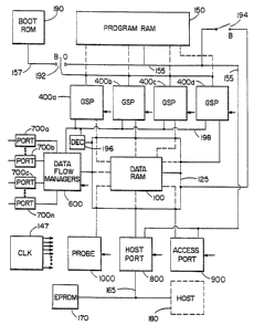
A high level block diagram of the preferred SPROC
subsystem 10 of the invention is seen in Figure 2. The
preferred SPROC 10 preferably includes: a central
"multiported" (as broai3ly understood) data RAM 100 accessed
via data RAM bus 125; a multiported program RAM 150 accessed
via program RAM bus 155; a plurality of internal processors
(G6P) 400 coupled to the data RAM bus 1.25 and the program RAM
bus 155 and which perform general processing functions; a data
flow manager (DFM) 600 which is coupled to the data RAM bus
125 and which generally controls the flow of data into and out
of the SPROC and relieves the GSPs from dealing with that data
flow; a plurality of serial data ports 70o coupled to the DFM
600; a host port 800 coupled to both the data RAM bus 125 and
the program RAM bus 155, the host port serving to couple the
SPROC via the host bus 165 to either an EPROM 170 in stand°
alone mode or to a host processor x80 in host mode; an access
port 900 coupled to both the data RAM bus 125 and the program
RAM bus 155; a probe 1000 coupled to the data RAM bus 125; and
WO 91t1~342 ~ ~~ ~ ;~ C'( ~ a~ pCT/1JS91/03386
an internal boot ROM 190 with boot ROM bus 157 coupled via
switch 192 to a GSP 400, the boot ROM 190 being used to
control a master SPROC 10 in start-up mode, as well as to
control the GSPs 400 of a SPROC 10 when the GSPs are in break
mode; and a flag generating decoder 196 coupled via flag bus
198 to the DFM 600 and the GSPs 400 for flagging the DFM and
GSPs when particular addresses of the data RAM 100 are being
addressed (as determined by values on the data RAM bus 125).
The SPROC 10 of the invention can function in several
different modes, some of which are determined by externally
set pins (not shown). In particular, the SPROC l0 has a boot
mode, an operational mode, and a development mode which
-w includes a "break" mode. In addition, the SPROC may be a
master SPROC or a slave SPROC which is either coupled to a
master SPROC (see Figure 11) or a host 180. In the boot mode
(powering up), Where the SPROC Z0 is a master, the SPROC l0 is
required to program both itself and any other slave SPROCs
which might be part of the system. To do that, upon power up,
sw~.tches 192 and 194 are toggled to connect to the B (boot)
nodes. With switches 192 and 194 so set, the boot ROM is
coupled to a GSP 400 such as GSP 400a, and the program RAM 150
is coupled to the data RAM bus 125. As boot ROM 190 is
coupled to the GSP 400a, the GSP 400a is able to read the boot
code in boot ROM 190. The code is arranged to cause the GSP
to seize control of the host port 800 and to load information
into the SPROC from EPROM 170 via the host port 800. The
information contained in EPROM 170 includes the program code
for the program RAM 150 (which is sent via data RAM bus 125),
configuration information for the DFM 600 and the serial,
host, and access ports 700, 800, 900, and parameter
information including initialization information for the data
RAM 100. This information, which was compiled by the
development system of the invention (as discussed in more
detail hereinafter) and stored in the EPROM, causes the SPROC
to perform the desired functions on data typically received
via serial ports 700.
L ? ~ PCT/US91/03386
WO 91 / 18342 ,~ . ,, i
11
In boot mode, after the master SPROC i.s programmed, the
remaining (slave) SPROCs of the system (see Figure 11) are
programmed by having the master SPROC 10 read the EPROM 170
and forward the information via the common host bus 165 to the
other SPROCs which reside in different address spaces. The
slave SPROCs do not require a boot ROM for boot mode purposes,
although the boot ROM 190 is also used to control the break
mode operation of the SPROC (as described with reference to
Figures 4).
After initialization is completed, boot mode is exited by
the writing of a predetermined value (fOH) to a predetermined
memory address (0401H) which causes switch 192 to toggle to
node O (operation), and switch 194 to-toggle to an open
position. Then the SPROC is ready to operate for its intended
signal processing purposes.
Although slave SPROCs may be programmed in boot mode by a
master SPROC, a slave SPROC may also be programmed~by a
microprocessor host such as host 180 of Figure 2. In slave
mode where a host such as host 180 is coupled to the host bus
165, the internal boot ROM 190 is not active. In fact,
switches 192 and 194 are set in the operating mode position.
In order to program the SPROC, the host 180 preferably
utilizes the host bus 165 and sends program data (possibly
obtained from EPROM 170) via host port 800, and program RAM
bus.155 to the program RAM, and data RAM data via host port
800 and the data RAM bus 125 to the data RAM. Configuration
information for the serial ports 700 and data flow manager
600, is sent by the host 180 via host port 80.0 and the data
RAM bus 125 as hereinafter described.
In operational mode, serial data flaw into and out of the
SPROC 10 is primarily through the serial ports 700, while
parallel data flows through the host port 800. Serial data
which is to be processed is sent into an input port 700 which
is coupled to the data flow manager 600, which in turn
forwards the data to appropriate locations (buffers) in the
data RAM 100. In certain circumstances, described below, the
DFM 600 will alsp write additional information to particular
data RAM locations which are monitored by flag generating
W~ 91/1342 c~ ~ ~.0~ ~~ ~~y ~ ~~ JPCf/U591/03385
12
decoder 196. Decoder 196, in turn, causes the flags to be
triggered over trigger or flag bus 198 as described below with
reference to Figures 13. Other flags are triggered by pulsing
hardware pins (not shown) via lines called "compute lines".
The hardware pins are particularly useful in providing
external timing information to the GSPs 400 and the DFM 600 of
the SPROC.
Once the data has been sent to the data RAM 100, and
typically after the GSPs 400 have been apprised via the flag
bus 198 of the arrival of the information, the GSPs 400 can
process the data. The processing of the data is conducted in
accord with one or more programs stored. in the multiported
program RAM 150 which in turn represents the functions,
topology, and parameters of a schematic diagram generated by
the user of the development system. In processing the data,
the GSPs 400 can read From and write to the data RAM 1.00.
Hawever, in order to shield the GSPs from T/O functions which
would interrupt and burden the GSPs, the GSPs do not address
each other directly, and do not read from or write to the DFM
600 or the input or output serial ports 700. Similarly, the
GSPs do not have direct access to the host port 800 or the
access,port 900. Thus, in order for the processed data to be
output from the SPROC 10, the processed data must be sent by
the GSP 400 to the data RAM 100. The data in the data RAM is
then either read by the DFM 600 and sent out serially via an
output port 700, or is sent out over the host bus 165 in a
parallel form via the host port 800.
The development mode of the SPROG device is used prior to
the final programming of the EPROM 170 and is basically
utilized in conjunction with a host 180. The development mode
permits a user to easily and advantageously develop an
integrated circuit signal processor by permitting the user
access to the internals of the SPROC device. For example, if
during a test operational mode it is desirable to obtain a
data "dump" of the registers of the GSPs, the GSPs 400 can be
put into break mode by causing a GSP to write to memory
address 406H. As a result of writing to that address, a
decoder (not shown) causes switch 192 to toggle, and
VSO 91/1$342 /", (~, ? jJ PCT/L'S91/03386
13
instructions from the break section of the boot ROM 190 are
used by the GSP 400 via bus 157. While boot ROM 190 is
coupled to the GSP 400 in this manner, the GSP runs a routine
which causes each register of the GSP to dump its contents to
predetermined 1~ dons in the data RAM 100. That data may
then be accessed. ~y the user and changed if desired via the
access port 900 or host port 800. Then, the break section of
boot ROM 190 reloads the data into the GSP, writes to memory
address 407H, and another decoder (not shown) causes switch
192 to toggle again such that the program RAM 150 is coupled
to GSP 400, and the program continues.
Other tools useful in the development mode of the SPROC
device are the access port 900 and the probe 1000: The access
port permits the user to make changes to the program held in
program RAM 150, ardor changes to parameters stored in the
program RAM 150 or the data RAM 100 while the SPROC is
operating. The probe 1000 pErmits the user to see.internal
signals generated by the SPROC in analog or digital form by
monitoring the values of data written to any particular data
RAM location. By using the access port 900 and the probe 1000
together, the effect of a change of a parameter value entered
via the access port 900 may be immediately monitored by probe
1000.
Before turning to the details of each of the blocks which
comprise Figure 2, it should be appreciated that central to
functioning of the SPROC is a multiported data RAM 100 and a
multiported program RAM 150. As aforementioned, the RAMS may
either be multip~rted by time division multiplexing a single
access to the RAMS (as seen by the solid lines of Figure 2) or
by providing true multiported RAMS (as suggested by the dashed
lines,of Figure 2). As indicated in Figure 3, in the
preferred embodiment hereof, access to the program RAM 150 by
the GSPs 400 and the host port 800 and access port 900 is via
time division anultiplexing of a single input. Similarly,
access to the data RAM 100 by the GSPs 400, the OFM 600, the
host port 800, the access port 900, and the .probe 1000 is also
via time division multiplexing of a single input.
VVO 91/18342 ~ 1~ ~ '~' «'' ~~ PCT/US91/03386
14
As seen in Figure 3, in the preferred embodiment of the
invention, there are five principle time slots of the basic
50MHz SPROC cloak 147 (shown in Fig. 2): one for each GSP; and
one shared by all of the other blocks of the SPROC. Each GSP
400 is able to read from the program RAM (p-rd) once over five
clock cycles, effectively providing each GSP with: a lOMHz
access to the program RAM 150. In the fifth clock cycle, the
host is given preferred access to either read from or write to
the program RAM. If the host does not need to read or write
to the program RAM, the access port is given access.
Alternatively; the host and access ports can be given 50/50
access to the fifth time slot by additional time division
multiplexing. ____
In the boot mode, only one GSP of the SPROC (e.g. GSP
400a) accesses the boat ROM 190. Because boot mode is used to
program the program RAM 150 with program data. from EPROM 170"
the program RAM bus 155 must be used by the GSP 400a for
writing to the pragram RAM 150 (via data RAM bus 12.5 and
switch 194). Thus, a program RAM write (p-wr) is provided as
shown in Figure 3 to allow for this situation (as previously
discussed with reference to Figure 2).
The data RAM 100 is similarly multiported via time
division multiplexing. As indicated in Figure 3, each GSP 400
is given a single time slot to either read or write from the
data R.AM 100. The fifth time slot (time slot 2) is subdivided
in time as follows: 50% for the host interface; and the
remaining fifty percent equally divided among the access port
900, each of eight sections of the DFM 600 relating to eight
serial ports 700, and the probe 1000.
The RAMS 100 and 150 of the invention are preferably
separate RAM devices and do not share memory space. For
example, the program RAM 150 is preferably a 1K by 24 bit RAM
which is assigned address locations 0000 to 03ff Hex. The
data RAM 100, on the other hand is preferably a 3K by 24 bit
data RAM with primary data RAM space of 2K assigned address
0800 to Offf Hex, and auxiliary register based space of 1K
assigned addresses 0400 to 07ff Hex. Of the primary data RAM
addresses, addresses 0800 through 0813 Hex relate to the
W~ 91/18342 ~ ~ ~ ~ L~ ~7 ~ PC.T/U591/03386
trigger bus flags as is discussed hereinafter, while addresses
0814 through Offf are used as data buffers, scratch pad
locations, etc. Of the auxiliary space, certain addresses are
used as follows:
0401H Exit boot mode (write fOH) (generate GSP hard
reset)
0405H Serial port reset (write)
0406H Global break entry (write) (generate GSP soft
reset)
0407H Global break exit (write) (generate GSP soft
reset)
0408H GSP1 break entry (write) (generate GSP soft reset)
0409H GSP2 break entry (write) (generate GSP soft reset)
040aH GSP3 break entry (write) (generate GSP soft reset)
040bH GSP4 break entry (write) (generate GSP soft reset)
040cF~ GSP1 break exit (write) (generate GSP~~soft reset)
040dH GSP2 break exit (write) (generate GSP soft reset)
040eH GSP3 break exit (write) (generate GSP soft reset)
040fH GSP4 break exit (write) (generate GSP soft reset)
0410H Serial Port 1 internal clock rate select
(write 00 = CK/2048) (write O1 = CK/1024)
(write 02 = CK/512) (write 03 = CK/256)
(write 04 = CK/128) (write 05 = CK/64)
(write 06 = CK/32) (write 07 = CK/16)
where CK is the SPROC clock (50 MHz)
0411H Serial Port 2 internal clock rate select
0412H Serial Port 3 internal clock rate select
0413H Serial Port 4 internal clock rate select
0414H Serial Port 5 internal clock rate select
0415H Serial Port 6 internal clock rate select
0416H Serial Port 7 internal clock rate select
0417H Serial Port 8 internal clock rate select
0440H to0447H Serial Port 1 (pradd = 0800H)
0448H to044fH Serial Port 2 (pradd = 0801H)
0450H to0457H Serial Part 3 (pradd = 0802H)
0458H to045fH Serial Port 4 (pradd = 0803H)
0460H to0467H Serial Port,S (pradd = 0804H)
0468H to046fH Serial Port 6 (pradd = 0805H)
0470H to0477H Serial Port 7 (pradd = 0806H)
0478H to047fH Serial Port 8 (pradd = 0807H)
0480H to0487H DAC (probe) input part (pradd = 0808H)
WO 91 / 18342 PC.'T/US91 /0338b
~i~~~.~~~)
16
0488H to 048fH DAC (probe) serial output port
04fcH to 04ffH Host interface registers
Memory locations 1000 to ffff Hex refers to external address
space (e. g. slave SPROCs, other devices, or memory).
of the auxiliary memory locations in the data RAM 100, it
should be noted that each GSP is given a break entry and break
exit data address. While the embodiment of Figure 2 causes
bus 155 to be connected to the boot/break ROM 190 when a break
is implemented such that all GSPs must break together,
different circuitry would allow for individual GSP breaks.
The eight twenty-four bit locations provided for each _
serial port are used to~configure the serial ports as well as
the DFM section associated with each serial port as
hereinafter described. Similarly, the eight words of memory
assigned the input and output ports of the probe are used to
configure the probe, while the eight words of memory assigned
the host port are used to configure the host port as described
hereinafter.
Further, with, regard to the memory locations, it is noted
that when information is~written to any of the serial part
locations indicated, another address (pradd), which turns out
to be a trigger flag address is generated by the DFM 600 (as
discussed' in more detail hereinafter) and written to the data
RAM bus 125. The writing of particular addresses to the data
RAM bus 125 is monitored by decoder 196. As seen in Figure.
13, the decoder 196 is logically comprised of an eleven input
AND gate 1210, sixteen six input AND gates 2020 - 2036, and
fifteen inverters 2050a - 20500. In essence, the first four
bits of the twenty-four bit data address written to data RAM
bus 125 are inverted by inverters 2050a - 2050d to select for
hexadecimal '°0". The fifth bit of the address is passed
directly to AND gate 1210, while the sixth through eighth bits
are inverted by inverters 2050e - 20508; the fifth through
eighth bits for selecting 'the hex address "8". The ninth
through eleventh bits are inverted by inverters 2050h - 2050j
to select in conjunction with a twelfth bit a hexadecimal "0"
or °'1", and the last five bits (the twelfth through sixteenth
I~VO 91/18342 fC1'/US91/03386
17
bits) are inverted by inverters 2050k - 20500, and the
uninverted and inverted states of the last five bits are
provided in different combinations, along with the output of
AND gate 2010, to the six input AND gates to provide an
appropriate positive output on trigger bus 198 should any of
addresses 0800 - 0813 be placed on the data bus 125 (i.e.
received by the decoder 196).
y Turning to Figure 4, a block diagram of the preferred
general signal processor (GSP) 400 of the.invention is seen.
The GSP is coupled to a program RAM 150 via program RAM bus
155. Because the program RAM 150 is preferably shared by a
plurality of GSPs 400, access to the program RAM bus is time
division multiplexed as indicated in Figure 3. The program
RAM bus 155 is comprised of a data bus of width twenty-four
bits, and an address bus of ten bit width where a 1K program
RAM is utilised. Of course, if a larger program RAM is
desired, additional bits are required to address the same, and
the program RAM bus would be wider. As indicated in Figure 4,
the GSP 400 writes to the address section of the program RAM
bus to indicate which instruction (RAM location) is desired.
However, under ordinary operating conditions the GSP 400 is
not capable of writing data to the program RAM 150. Under
ordinary operating conditions, data is written into the
program RAM 150 only via the host or access ports shown in
Figure 2 which are also coupled to the program RAM bus 155 in
a time division multiplexed manner.
The GSP 400 is also coupled to the multiported data RAM
100 via a data RAM bus 125. Because the data RAM 100. is
central to the processor architecture, and because non-
~ arbitrated access to the data RAM 100 is desired, the data RAM
100 must either be a true multiported data RAM, or access to
the data RAM 100 via the data RAM bus 125 must be time
division multiplexed so as to effectively create a multiported
RAM. The data RAM bus preferably comprises a data RAM address
bus of sixteen bit width, an a data RAM data bus of twenty-
four bit width. As indicated in Figures 3 and 4, the GSP may
write to the address section of the program RAM 100. Also,
'~~~~~i~~~
~'O 91 /18342 "' PC,"T/US91 /03386
18
the GSP may both read and write to the data section of the
data RAM bus.
The GSP is substantially described by the details and
functioning of six sections: a block controller 410; a program
control logic block 420; a multiplier block 430; an ALU block
450; a flag block 460; and a data IdAM address generator block
470. Coupling all six sections, as well as a break register
492, a data access register 494, and a temporary register 496
is an internal twenty-four bit bus 490. A11 access from any
of the sections or from the registers 492, 494, or 496 onto
the internal bus 490 is wia tristate drivers 429, 449x, 449b,
459, 469, 489, and 499.
Block controller 410 is comprised of instruction decoder
412, and sequencer 414. The instruction decoder 412, when
enabled, takes fourteen bits (nine bits of opcode, and five
bits of operand) off of the data portion of the program RA14
bus. Six of the nine opcode bits are used to indicate the
operation (instruction) which the GSP is to perform (e. g. add,
shift, jump, etc.), with up to sixty-four instructions being
accommodated. In the preferred embodiment an additional three
bits of opcode are utilized to specify the addressing mode the
GSP is to use. In particular, in the "absolute" mode (code
000), the fifteen bits in the O register 472 of the address
generator black 470 are used to select an address in the data
RAM 100,-and the data in that address of data RAM is used for
the operation. In the "register" made (code 001), the five
operand bits obtained by the instruction decoder 412 are used
to specify which register of the numerous registers of the GSP
is to place its contents onto the internal bus 490. In the
"immediate left" mode (code 010), the fifteen bits of data in
the O register are to be put into the fifteen msb slots of the
internal bus 490, while in the "immediate right" mode (code
011), the fifteen bits are put into the fifteen lsb slots of
the internal bus. Tn the remaining four modes, "BL index2d'°
(Code 100), °°B indexed°' (Code 101), °'FL
indexed" (COde 110),
and !'F indexed" (code 111), 'as described in more detail
hereinafter, values in base registers B or F are added to the
value of the fifteen bit operand stored in the O register and,
130 91/18342 ~ ~ ~ ~ ~ fCT/US91/U3386
19
where appropriate, to the value in the L (loop) register, and
are output onto the data RAM bus 125.
Instruction decoder 412 is not only coupled to the
program RAM bus, but to the numerous multiplexers, tristate
drivers, registers, etc. of the GSP via lines 416. Hased on
the instruction which is decoded by instruction decoder 412,
various of those lines 416 are enabled in a sequence as
determined by the sequencer 414. Tn effect, instruction
decoder 412, and sequencer 414 are simply look-up charts,
with instruction decoder 412 looking up which lines 416 must
bs enabled based on the code found in the nine bits of opcode,
and sequencer 414 looking up the sequence to which the enabled
lines must subscribe.
While instruction decode._ 412 decodes whatever
instruction is on the program RAM bus 155 when the GSP 400 is
granted~access to that bus, the instruction which is on the
bus is generated and dictated by the program logic~block 420.
Program control logic block 420 is comprised of a tristate
driver 422, a program address value register 424 (also called
the "P" register), an incrementer 425, an increment (I)
register 426,. a jump (J) register 428, a multiplexer 430, and
a branch logic block 432. The P register 424 contains the
location of the program RAM 150 which contains the
microinstructions which are to be used by the GSP 400. P
register 424 writes that address onto the program RAM bus 155
by sending it to tristate driver 422 which acts as the bus
interface.
Updating of the P register 424 is accomplished via muxP
430 which chooses one of the twe:..ve bit addresses stored in
the I register 426 or the J register 428 based on information
from branch logic block 432. the address stored in the I
register is simply the next numerical address after the
address stared in the P register, as a value of one is added
at incrementer 425 to the value stored in P register 424. In
most situations, muxP 430 will permit the P register 424 to be
updated by the T register, and the sequential addressing of
the program RAM will continue. However, in some situations,
such as where a jump in the routine is desired, the
WO 91/i8342 ~ ~~ ~ ~ ~ . PCT/US91/0338b
~~ ~7i,~j
multiplexer 430 will permit the address in the J register 428
to be loaded into the P register 424. ' The decision to jump is
made by the branch logic block 432 which reads the status of a
plurality of status flags as is hereinafter discussed. The
address to which the jump is made is obtained by the J reg 428
from the internal bus 490, which may obtain the address from
any of the sections of the GSP 400 (or from the data RAM 100).
Coupled to the program control logic block 420 is a break
register 492 in which upon the execution of a break
instruction is loaded status flag information as well as the
value of the P register plus one. The status flag arid P
register inf~rmation is stored in the break register 492 which
-~is coupled to internal bus 490 via tristate driver,429 because
it is otherwise not available for placement on to the internal
bus 490. A program break is typically executed when an
information dump is desired by the system user, and is
accomplished by putting an instruction in the program RAM 150
which causes the GSP 400 to write to a certain address (e. g.
0406H) of the data RAM 100. A decoder (not shown) on the data
RAM bus 125 is used to determine that the program break is to
be executed (based on the location to be written to), arid a
control signal is provided by the decoder to the break
register 492. The program break instruction in the program
RAM 150 causes instructions in a boot/break ROM 190 (shown in
Fig. 2) which is coupled to the program RAM bus 155 to be
accessed by the program control logic block 420. The
instruction code in the boot/break ROM 190 in turn causes the
values of each of the registers in the GSP 400 to be written
into desired locations in the data RAM 100. Then the GSP 400
. is kept waiting until the wait flag stored in its wait flag
register (discussed below) is cleared. During the wait
period, if desired, the user can change the values of data in
the data RAM as described in more detail below with reference
to the access port 900. Then, when the wait cycle is
terminated, the instructions in the boot/break ROM 190 causes
the values in~the data RAM, including any new values, to be
written back to their appropriate registers in the GSP. The
location of the next desired microinstruction contained in a
9~'O 91/18342 PCT/U~91/03386
21
program RAM 150 location is loaded into the P register, so
that the GSP can continue in its normal fashion.
The multiplier block 430 and the ALU block 450 of the GSP
perform the numerical computations for the GSP. The
multiplier block 430 is comprised of two input registers Xreg
432 and Yreg 434, a multiplexer 436 which is coupled to the
internal bus 490 via tristate driver 449a, a multiplier 438
with a post Xreg 439, and a multiplier control 441, a summer
442, an output register Mreg 444, and a second multiplexer 446
which selects which of six words is to be output onto internal
bus 490 via tristate driver 449b. Typically, the
multiplicand is loaded into Xreg 432. Then the multiplier is
~lor~ded into Yreg 434 while the multiplicand is loaded into
post Xreg 439. The multiplier control 441 permits the
multiplier 438.to function over several machine clock cycles
(e. g. three clock cycles totalling 300 nanoseconds = fifteen
internal GSP cycles). If in multiplying, the multiplier
overflows, a status flag M is set, and this information is
conveyed to the branch logic block 432 of the program logic
section 420. Regardless, the product of the multiplier and
multiplicand is forwarded to summer 442 which, in a multiply
with accumulate mode, adds the new product to the sum of
previous products and forwards the sum to the multiply
register M 444. In a pure multiply mode, the contents of the
summer are cleared so that the product is forwarded through
the summer which adds zera and send the product to the M
register.
The contents of the M register 444 are available to the
internal bus 490. However, because the M register can
accommodate a fifty-six bit word, and the internal bus 490 is
a twenty-four bit bus, only a portion of the M register word
may be placed on the bus at one time. Thus, multiplexer 446
is provided to either select the twenty-four least significant
bits (lab's) in the M register, the twenty-four next lab's in
the M register, or the eight most significant bits (msb's) in
the M register. If the eight msb's are chosen, the eight
msb's are placed in the eight lab slots of the internal bus
490, and the msb of the eight bits is extended through to the
WO 9Y/~834z ~ ~ ~ ~ ~~ ~ ~~ PCT/US91/03386
22
msb slot on the bus (e. g. if the msb is a "1°', the first
seventeen msb's on the bus will be "1"). The multiplexes 446
is also capable of selecting a left shifted by two (zero
filling the right) twenty-four or eight bit word. Thus, in
all, multiplexes 446 can provide six different outputs based
on the product in the M register 444.
The ALU block 450 of the processor is basically a
standard ALU, having an arithmetic-logic unit 452 with input
register 454, and an output accumulator register 456. The
arithmetic-logic unit 452 is capable of the standard functions
of similar units, such as adding, subtracting, etc., and
produces values for Areg 456, as well as status flags
including carry (C), overflow (O), sign bit (S), and zero (Z).
The status flags are used by the branch logic block 432 of the
program logic block 420 to determine whether a conditional
jump in the microcode program should be executed. The Areg
contents are output onto internal bus 490 via tristate driver
459.
Wait flag block 460 is comprised of two wait flag
registers WFreg 462 and DFreg 464, a multiplexes 466, and OR
gate 468. The bits of the wait flag registers may be set
(i.e. written to) by data sent over the internal bus 490.
Also', .registers WFreg 462 and DFreg 464 are coupled to a flag
bus 198 which is written to each time predetermined locations
in the data RAM 125 are addressed as hereinbefore described
with reference to Figures 2 and 13. In this manner, each bit
of the wait flag registers 462 and 464 may be selectively
cleared. When all of the bits in register WFreg 462 have been
cleared due to the occurrences of specified events (e.g. the
data RAM has received all the information which is required
for another computation), OR gate 468 is used to provide a
status flag W which indicates the same. Status flag W is read
by the .branch logic block 432. In this manner, "jump on wait
flag" commands may be executed.
The DFreg 464 of the wait flag block 460 functions
similarly to the the WFreg 462, except that no signals
indicating the presence of all zeros (or ones) are output by
the DFreg. In order to check the contents of the DFreg (or
WO 91/1342 PCT/USh1/03386
a~ 1J '
l~ ~ t'~J '~' '~ ~~ ~ 1.~
23
the WFreg, if all values in the WFreg are not zero), the
register must be selected to put its contents on the internal
bus 490. The selection of one of the registers is made by the
instruction decode 412 and sequences 414, and the contents are
forwarded via multiplexes 466 and the tristate driver 469. An
easy manner of determining whether the DFreg 464 has all zeros
is to forward the contents of the DFreg 464 to the ALU 452,
which will provide a status flag Z if the contents are zero.
The final large block of the general signal processor is
the data RAM address generator block 470 which includes bus
wide OR gate 471, registers Oreg 472, Dreg 473, Lreg 474, Breg
476, Freg 477, adders 481, 482, and 483, multiplexers muxBFL
484, ~muxL 485, muxA 486, muxBF 487, mux0 488, and'an address
access block 489. As previously indicated, the Oreg 472
obtains the fifteen least significant bits of the instruction
on the program RAM bus. If °°absolute" addressing is desired,
i.e. the address to be written onto the data RAM bus is
included in the program RAM microinstruction itself, the
address is written into the Oreg 472, and then forwarded to
the data RAM bus (a sixteenth bit having been added by a zero
extender, not shown) via muxA 486 and the address access block
489. The sixteen bit address is then placed on the data RAM
bus at the appropriate time. All other situations constitute
''indexed°' addressing, where the address to be put out on the
data RAM bus is generated internally by the data RAM address
generator block 470.
Addresses are generated by adding the values in the
various registers. In particular, and as indicated in Fig. 4,
the Oreg 472 is the offset register, the Dreg 473 is a
decrement register, the Lreg 474 is a loop register which sets
the length of a loop, the Breg 476 is a base address register,
and the Freg 477 is a frame address register which acts as a
second base address register. The 0 register obtains its data
off of the program RAM bus, while registers D, L, B arid F
obtain their data from the internal bus 490. If it is desired
to add some offset value to the value in the base or frame
register (i.e. the "B indexed mode" or "F indexed mode") in
order to generate an address, muxBF 487 selects appropriately
W091/183a2 ~ ~ ~ ~ y?~ ~~ P~1'/U~91/03386
24
the Breg 475 or the Freg 477, muxBFL 484 selects the value
coming from muxBF 487, and the Breg or Freg value is added to
the offset value of the Oreg by the adder 483. That value is
then selected by muxA 486 for output over the data RAM bus via
the address access block 489. Similarly, if it is desired to
add some offset value and some loop value to the value in the
base or frame register (i.e. the "BL indexed mode" or the "FL
indexed mode"), the value in the L register is added to the
value in the B or F registers at adder 482, and the sum is
passed via muxBFL 484 to adder 483 which adds the value to the
value in the O register.
By providing adder 481, and by coupling.the decrement
register Dreg and the loop register Lreg to the adder 481,
registers an address loop is effectuated. In particular, the
Lreg sets the length of the loop, while the Dreg sets the
value by which the loop is decremented. Each time the Dreg is
subtracted from the Lreg 475 at adder 481, the new value is
fed back into the Lreg 475 via muxL 485. Thus, each time a
DJNE instruction is executed (as discussed below), the
resulting value in the Lreg is decreased by the value of the
Dreg. If added to the Breg or Freg, by adder 482, the address
generated is a sequentially decrementing address where the
value in the Dreg is positive, and a sequentially incrementing
address where the value in the Dreg is negative.
The ability to loop is utilized not only to provide a
decrementing (or incrementing) address for the data RAM bus,
but is also utilized to effect changes in the program RAM
address generation by providing a °°decrement and jump on not
equal" (DJNE) ability. The output from the adder 481 is read
by oR gate 471 which provides a status flag L (loop) to branch
logic block 432. The status flag L maintains its value until
the L register has looped around enough times to be
decremented to the value zero. Before that point, when the
Lreg is not zero, the next instruction of the G~SR is dictated
by the instruction indicated by the Jreg 428. In other words,
the program jumps to the location of the Jreg instruction
instead of continuing with the next instruction located in the
I register. F3owever, when the Lreg does decrement to the
W~ X1/18342 PC'I'/US91/033F36
I~~~~~~~~
value zero, the OR gate 471 goes low a d toggles flag L. on
the next DJNE instruction, since the not equal'° state does
not exist (i.e. the Lreg is zero), branch logic 43z causes
muxP 430 of the program logic block 420 to return to obtaining
values from the Ireg 426 instead of from the Jreg 428, and the
program continues.
The values of any of the O, D, L, B, or F registers may
be placed on the internal bus 490, by having mux0 488 (and
where appropriate mux BF 487) select the appropriate register
and forward its contents via tristate driver 489 to the
internal bus.
Coupled to.the.internal bus. 490, and interfacing the _.._
internal bus 490 with the data slots on the data RAM bus is
the data access port 494. The data access port 494 is capable
of reading data from and writing data to the data RAM and is
given access to the data RAM in a time division multiplexed
manner as previously described. In writing to the~data RAM,
the data access part 494 and the address access port 489 are
activated simultaneously. In reading data from the RAM, the
address access port 489 first places on the data RAM bus the
data RAM address in which the desired data is stored. The
data is then placed on the data RAM bus by the data RAM, and
the data access port 494 which is essentially a dual tri-state
driver, receives the data and passes it onto the internal bus
490 for storage in the desired GSP register.
If desired, additional registers such as~ Z register 496
may also be coupled to the internal bus 490, and may be used
as temporary storage. The contents of Zreg 496 are output
onto the internal bus 490 via tristate driver 499.
The functioning of the GSP is well described by the
following microcode example which is provided for purposes of
description onlyo
INST # HEXCODE LABEL ASSEMBLY CODE COMMENTS
$START
0000 498008 LDWS #8 initialize wait reg.
0001 (98001 $WAIT JWF $WAIT wait until RAM address
803H is written to
WO 91/8342 ~ ~~ ~ i fCT/US91/43386
~: ~ ~'',j
26
0002 348001 LDD #1 set Dreg (decrement)
to
1
0003 458007 LDL #7 set Lreg (loop) to
7
0004 358824 LDB #824H set Breg (base) to
HEX
824
0005 318000 LDA #0 initialize ALU
accumulator
$LOOP
000 6 120000 ADD (B+L] add the 8 numbers in RAM
0007 f48006 DJNE SLOOP locations HEX 82b...824
0008 f1800b JGE $POS test accumulator and
jump
if positive
0009 240000 NOT else take 1's complement
of accumulator
000a 118001 ADD #1 add 1 to 1's complement
$POS
OOOb 4c800e LDX A load accum. into Xreg
OOOc 542666 MPY #1.2 multiply Xreg by 1.2
OOOd 740000 NOp no operation permits
OOOe 740000 NOP multiplier to complete
000f 498012 JMF $ERRORtest overflow flag
M
and jump if error
0010 a40823 STMH 823H store result in RAM
location 823H
0011 c58000 JMp $ START return to $START
0012 318000 $ERROR LDA #0 On error, Store 0 in
.
0013 900823 STA g23H location 823H
0014 c58000 JMP $STARTreturn to $START
END
The first instruction (0000) causes the wait register to
be loaded with the value eight. Instruction 0001 causes the
GSP to wait until. the trigger flag address of 803H is written
to by another GSP or by other circuitry of the system.
Instruction 0001 accomplishes the wait by telling the GSP to
jump to instruction 0001 (i.e. repeat itself) until the wait
flag (i.e. controlled by writing to address 803H) is toggled.
Once the wait flag is toggled, instructions 0002 - 0004 set
the D, L and B registers of the data RAM address generator
9~V~ 91 /18342 r ~C f/U591 /U338b
~1~('~~ ~ ~~
27
block 470. By setting the loop register to a value 7, and the
D register to value 1, the loop will executed eight times.
Instructions 0006 and 0007 comprise the loop.
Instruction 0006 requires that the value in the base and loop
registers be added together by adder 482, added to a zero
value contained in the Oreg 472, and placed onto the data RAM
bus. The value at data RAM location B+L is then placed onto
the data RAM bus, forwarded through data access block 494 into
the ALU 452, and accumulated in the A register 456. The DJNE
assembly code command of instruction 0007 looks to see whether
the L flag has been toggled. If not, the L register is
decremented by the value in the D register, and the program
jumps back to SLOOP; i.e. instruction 0006 which adds the new
value of L to the value in the B register and places that onto
the data RAM bus. The value at that data RAM location is then
placed onto the data RAM bus, forwarded through the data
access block 494, added in the ALU with the value in the A
register 456, and stored as an accumulated value in the A
register 456. This procedure conwinues until L is equal to
zero and the L flag is toggled. Then upon reaching
instruction 0007, no decrement or jump is executed. Rather,
the program continues to instruction 0008.
At instruction 0008 the value in the Areg 456 is tested
by looking at the status flags of the ALU 452. If the value
is positive, the program jumps to instruction 000b (whose
address was placed in the Jreg 428). If not, instructions
0009 and 000a are carried out. At 0009, the one°s complement
of the accumulator is taken by the ALU 452, and at step 000a,
the value one is added. In this manner a two's complement of
the value in the accumulator is provided.
At instruction OOOb, the positive value of the
accumulator, or the two's complement generated is loaded from
the Areg 456 into the Xreg 432 of the multiplier block 430.
Instruction OoOc causes the value in the Xreg 432 to be
multiplied by the value 1.2. Because a multiplication
function requires numerous steps and several cycles,
instructions OOOd and OOOe are NOP (no operation)
instructions, which permits the multiplier of the GSP to
WO 93!18342 PCT/US91/03386
~~ 9~~~~~'~
28
complete the calculation before continuing the program.
However, if it was desired to conduct an arithmetic or logic
calculation in the ALU section 450, or to write a value to or
fetch a value from the data RAM, the GSP could conduct
concurrent operations, provided the multiplier section 4~0 was
not involved.
Instruction OOOf tests the multiplier overflow flag M.
If the multiplier overflowed due to the multiplication, an
error is flagged and the program jumps to instruction 0012.
If there is an error, instruction 0012 loads the value zero
into the A register 456 of the ALU block 450. Then, at
instruction 0013, the value of the A register is written to
location"823H of-the data RAM. The entire program is
restarted by instruction 0014 which jumps back to instruction
0000 which places the GSP into the wait state. If there is no
error indicated by flag M, instead of jumping to instruction
0012, the program continues with instruction 0010..
Instruction 0010 causes the value in the Mreg 444 to be stored
at RAM location 823H by having the value written to the
internal bus 490 and then out onto the data RAM bus via data
access port 494. Instruction 0011 then causes a jump back to
the start of the program (instruction 0000) which places the
GSP in the wait state.
Additional understanding of the GSP may be had by
reviewing the assembly code and operands of a sample function
accomplished by the GSP. In particular, the following
eighteen cycle instruction set comprises a listing for biquad
filter having the structure seen in Fig. 5. In Fig. 5, an
input value x is multiplied by multiplier 504 by parameter
value ib0 stored in block 506. The previous x value delayed
by delay block 512 is shown as x1 and is multiplied at
multiplier 514 by parameter value ibl taken from block 516.
The x value previous to the x! value which was further delayed
by delay block 522 is shown as x2 and is multiplied at
multiplier 524 by parameter value !b2 taken from block 526.
The products of ib0 times x, ibl times x!, and ib2 times x2
are summed by summation block 530 along with additional values
generated from the output of summation block 530. Thus, the
WO 91/18342 PCf/US91 /03386
29
previous output y delayed by delay block 532 and is shown as
y1. The y1 value is multiplied at multiplier 534 by parameter
value ial from block 536 and added by summation block 53o to
the other products. Similarly, the output previous to y1
which was further delayed by delay block 542 is shown as y2.
The y2 value is multiplied at multiplier 544 by parameter
value ia2 taken from block 546 and is further added to the
other products.
The blockdiagram the biquad which includes parameter
of
values and ia2, and changing variables
ib0, x1,
ibl,
ib2,
iai
x2, y1, may be
and implemented
y2 by the
GSP as
the following:
LINE ASSEMBLY COMMENTS
# CODE
1 LDX x2 Load X reg with sample x2
2 MPY ib2 Multiply x2 times ib2
3 NOP No operation
4 LDX x1 Load X reg with sample x1 while
multiply continues
MAC ibl Multiply x1 times ibl and accumulate
with x2 times ib2
6 STX x2 Store the value in the X reg (x1)
into
location x2 for next computation
7 LDX [in] Load the X reg with data at addr.
[in]
while previous multiply. continues
8 ' MAC ib0 Multiply [in] value times ibo and
accumulate with other values
9 STX x1 Store the value in the X reg ([in])
in location x1 for next computation
LDX y2 Load X reg with sample y2
11 MAC ia2 Multiply y2 times ia2 and accumulate
with other values
12 NOP No operation while waiting for
multiply
13 LDX y1 Load X reg with y1 while multiply
continues
14 MAC ial Multiply y1 times iai and accumulate
with other values
STX y2 Store the value in the X reg (y1)
in
WO 91/18342 ~ ~ U ;.s ~~ ~a ~~ PCT/U591/03386
location y2 for next computation
16 NOP No operation while waiting for
multiply
17 STIR y1 Store the high section of the Mreg
accumulated value~at lacation y1
for
next computation
18 STMH Cout] Store the high section of the Mreg
accumulated value at the output
locale
Lines 1-3 of the code cause the multiplier of the GSP to
multiply the x2 value (i.e. the value stored in location x2)
by parameter value ib2.Lines 4.and 5 of the code cause the
multiplier to multiply the x1 value (i.e. the value stored in
location x2) by parameter value ibl and to add the product to
the product of x2 and ib2. Line 6.of the code moves the x1
value into the x2 location so that the next time the code is
executed (e. g. when a new x value is received) the.~C1 sample
will become the x2 sample (i.e: delayed by one total cycle).
Lines 7 and 8 of the node cause the multiplier to multiply the
new x value (xin) by ib0 and to add the product to the
previously accumulated~products. Line 9 of the code parallels
line 6 of the cads by moving the present input value (xin)
into the x1 location so that the next time the code is
executed the new x value becomes the delayed x1 value.
Lines IO-l2 of the bic~uad code cause the multiplier of
the GSP to multiply the twice delayed output value y2 by
parameter value ia2 and to add that product to the previously
accumulated products, while lines 13 and 14 cause the
multiplier to multiply the one delayed output value y1 by
parameter value ia1 and add that to the previously accumulated
products. Line 15 causes the GSP to~store the y1 parameter
value into location y2 for the next time the code is executed,
while lane I6 conducts no operation, thereby permitting the
multiplication of y1 and ial and the adding of its product to
the accumulated products to complete. Line 17 causes the sum
in the accumulator,(ib0 times x, plus ibl times x1, plus ib2
times x2, plus ia1 times y1, plus ia2 times y2),to be stored
W~ 91/18342 PCT/US91/03386
31
in the y1 location for the next execution of tine code, while
line 18 takes the same sum and puts it i.n an output location
as the output of the biquad.
Turning to Figures 6a, 6b, and 6c, block diagrams of the
input and output circuitry of the data flow manager (DFM) 600
of the invention, and an example FIFO related to the DFM are
seen. As previously described, the DFP4 serves the important
function of handling the flow of data into and out of the
processor apparatus so that GSPs of the processor apparatus
need not be interrupted in their processing tasks. In
accomplishing this function, the DFM takes data received by
the serial port from the "world" outside of the particular
-processor apparatus and organizes.it inside a FIFO such as~the
FIFO of Fig. 6c Which is implemented in desired locations of
the data RAM 100 of the SPROC apparatus 10. Also, the DFM 600
takes data in a FIFO, and organizes it for output to a serial
output port of the SPROC apparatus. The DFM is also capable
of directing data i:~to a FIFO and drawing data from a FIFO at
desired speeds_so,as to accommodate a decimation operation
performed by the SPROC. 'Further, the DFM causes decoder 196
to write glags to the flag bus 198 (and hence to the GSPs 400)
of the SPROC apparatus ZO regarding the status of the buffers.
The DFM 600 of the SPROC apparatus may either be central
to the apparatus, or distributed among the serial input and
output ports 700 of the apparatus, with a single DFM serving
each port 700. Where distributed, the circuitry seen in block
diagram form in Figures 6a and 6b is duplicated for each
serial input and output port 700 of the SPROC apparatus,
,although certain circuitry could be common if desired.
The circuitry for receiving data from a serial port and
organizing it for storage in a FIFO of the data RAM 100 is
seen in Figure 6a. The data flow itself is simple, with the
data being sent from the serial port 700, via multiplexer 611
and tri-state driver 613 to the data slots of the data RAM bus
125. Multiplexer 611 permits either data coming from serial
port 700a or data generated as hereinafter described to be
forwarded to driver 613. Driver 613 is controlled as
indicated such that data is only output on the data RAM bus
~0 9aias3az ~, ~ ~ ~=~. e~ ~' ~~ pcricrsnaio~~sb
32
125 when the DFM 600 is enabled by the system-wide multiplexer
clock scheme. The organization of the data for output onto
the data RAM bus as a twenty-four bit word is conducted by the
serial port 700, as hereinafter described.
Besides the data flow circuitry, each DFM is arranged
with buffers, counters, gates, etc. to generate data 32AM FIFO
addresses for the incoming data. As shown in Figure 6a, the
DFM 600 has three registers 620, 622, 624, three counters
630, 632, and 634 associated with the three registers, an
adder 636, a divide by two block 637, a multiplexer 638, seven
logic gates 641, 642, 643, 644, 645, 646, and 647 (gates 642,
643, 645, and 647 being bus wide gates), and two delay blocks
648 and 649. The three registers are respectively: the start
of FTFO register 620 which stores the start location in the
data RAM for the FIFO to be addressed by the particular serial
port coupled to the particular part of the DFM~ the index
length register 622 which stores the number of buffers which
comprise the FIFO (for the FIFO of Fig. 6c, the index length
register would be set at four), and the buffer length register
624 which stores the length of each buffer, i.e. the number of
words that may be stored in each buffer (for the FIFO of Fig.
6c, the buffer length register would be set at eight). When a
data word (twenty-four bits) is ready for sending to the data
RAM for storage in a FIFO, the serial port 700a provides a
ready signal which is used as a first input to AND gate 541.
The second input to AND gate 641 is a data enable signal which
is the time division multiplexed signal which permits the DFM
to place a word an the data RAM bus. With the data enable and
ready signals high, a high signal is output from the AND gate
.which causes driver 613 to output the data on the data RAM bus
along with an address. The address is that which is computed
by the twelve bit adder 636, or a prewired address, as will be
described hereinafter.
When AND gate 641 provides a high output, the high output
is delayed by delay blocks 648 and 649 before being input into
clock counters 630 and 634. As a result, counters 630 and 634
increase their counts after an address has been output on the
data RAM bus. When counter 630 increases its count, its count
h '
1%V0 91/183x2 ~ ~ ~ l ~ ~ 3~ PCf/U591/03386
33
is added by the twelve bit adder 636 to the FIFO start
location stored in register 620. If selected by multiplexes
638, the generated address will be the next address output in
the address slots of the data RAM bus in conjunction with the
data provided by.driver 613. Thus, as data words continue to
be sent by the serial port for storing in the data RAM FIFO,
they are sent to incremental addresses of the data RAM, as the
counter 630 increasingly sends a higher value which is being
added to the FIFO start location. As is hereinafter
discussed, the counter 630 continues to increase its count
until a clear counter signal is received from circuitry
associated with the index length register 622. When the clear
counter signal is received, the counter starts counting again
fr~ .m zero.
As aforementioned, each time the AND gate 641 provides a
high output, the counter 634 associated with the buffer length
register 624 is also incremented (after delay). The outputs
of the buffer length register 624 and its associated counter
634 are provided to bus wide XNOR gate 643 which compares the
values. When the counter 634 reaches the value stored in the
bu..~er length register 624, a buffer in the data RAM FIFO has
been filled. As a result, the output of XNOR gate 643 goes
high, causing three input OR gate 644 to pass a high signal to
the reset of counter 634. The high signal from bus wide XNOR
gate 643 is also fed to the counter 632 associated with the
index length register 622, to the multiplexes 638, and to the
multiplexes 611. As a result of the buffer being filled,
multiplexes 638 enables the prewired address to be placed in
the address slots of the data RAM bus 125, along with one of
.two predetermined (or generated) data words which are
generated as discussed below. The placement of the prewired
address and a data word on the bus at the end of buffer signal
occurs upon the next data enable signal received by the DFM,
which is before another word is assembled by the serial port
TOOa for sending to the data RAM 100. Also, the placement of
the prewired address and data word is used for signalling
purposes, as a decoder 196 (seen in Figure 2) monitors the
data RAM bus 125 for the particular prewired addresses of the
l7FMs; the triggering of these addresses occurring because of
WO 91/18342 1~CT/US91/03386
34
conditions in the DFM, i.e. the filling of buffers. The
decoder 196 in turn, can set a flag (the setting of the flag
can be dependent on the value of the data accompanying the
prewired address) on the trigger bus 198 which signals the
GSPs 400 of the SPROC of the occurrence. In this manner, the
GSPs 400 can determine that the data required to conduct an
operation is available to the GSP, thereby causing the GSP to
exit a wait loop.
The predetermined or generated data word placed on the
bus after a FIFO buffer has been filled preferably uses a "1"
as the msb of the data word if the FIFO buffer that has been
filled causes the FIFO to be half filled (as described
hereinafter), or a "0'° as the msb otherwise. The remainder of
the data word may be null information. Or, if desired, the
data word may include the next location to which the DFM will
write (i.e. the location computed by the twelve bit adder 636)
which is inserted in appropriate locations of the data word.
This predetermined or generated data word is then passed via
multiples 611 to driver 613 which places the data word on the
bus at the same time the prewired address is placed on the
data RAM bus 125.
As aforementioned, when an indication of a full buffer is
output by bus wide XNOR gate 643,. counter 632 is incremented.
Counter 632 therefore tracks the number of the buffer in the
FIFO that is being filled. When the number of the FIFO buffer
being addressed (as determined by counter 632) is half of the
FIFO length (as determined by the length stored in register
622, divided by divide by two block 637), a flag is raised by
.the DFbI via the bus wide XNOR gate 647. The "mid buffer" flag
indicates that the buffer in the FIFO being written to is
halfway through the FIFO. Hence, if all previous buffers in
the FIFO are still full with data, the FIFO is half full. In
addition, the mid buffer flag causes the generated data input
to multiplexes 611 to be changed, such that the msb of the
data is a °'1" instead of a zero. Thus, upon filling the
buffer which causes the FIFO to be half filled, a slightly
differently coded data word is placed in the data slots of the
data RAM bus.
'WO 91118342 ~ ~ ~ ~ ~ '~'~ PCf/L'S91/033~6
When the v~a~.ue of counter 632 is incremented to the value
stored in the index length register 622, the last location in
the FIFO has been addressed. Accordingly, it is desirable to
recirculate; i.e. to continue by addressing the first location
in the FIFO. With the value of counter 632 equal to the value
of register 622, bus wide XNOR gate 645 provides a high signal
which is passed through three input OR gate 646. As a result,
counters 630, 632, and 634 are reset. As indicated in Fig.
6a, a "clear counter" signal may also be generated by a power
up reset (PUR) signal which is generated by applying a signal
to a predetermined pin (not shown) of the SPROC, and by a SYNC
signal which is generated by writing to address 0405H of the
_. . data RAM 100. The SYNC signal permits different DFMs to- be
synchronized to each other.
If desired, the input section of one DFM can be
synchronized to the output section of the same or another DFM.
This synchronization is accomplished via a pin (not shown) on
the SPROC which generates the "en buf'° input into OR gate 644.
In turn, OR gate 644 provides a high signal which resets
counter 634 in synchronization with the resetting of a similar
counter in a DFM output section such as described with
reference to Fig. 6b.
Turning to Fig. 6b, the serial output section of the DFM
600 is seen. The function of the output section of the DFM is
to take data in the FTFO, and organize it for output to a
serial output port 700b of the SPROC apparatus.
The output section of the DFM is preferably comprised of
several registers and counters, logic elements including AND
gates, comparators, and inverters, divide and add blocks,
flip-flops, a buffer and a parallel to serial converter.
Basically, the data flow through the serial output section of
the DFM is simple. An address generated by the the start
address register 652 is added by adder 654 to the value in the
offset counter 656, and that address is output onto the
address section of the data RAM bus. The data RAM receives
the address information and then places the data located at
that data RAM address an the data R1~M bus. That data is
WO 91!18342 , n ,~ ~~ ~ ~ f'C'T/US9i/03386
~~~~s~.v~
36
received by the DFM and latched and stored in buffer 694 prior
to being forwarded to the serial output port 700b.
The remaining circuitry of Fig. 6b serves the functions
of not permitting the data to be forwarded to the serial
output port 700b unless certain conditions (i.e. triggers) are
met, as well as generating synch pulses and error flags
depending on internal logic and received signals. In
particular, each DFM has a wait register 660 which holds flag
information which must be cleared in the wait flag register
662 before a signal will be generated. The bits in the wait
flag register are only cleared upon receipt~of appropriate
trigger bits received from the trigger bus 198. When the
appropriate flags are-cleared, bus wide NOR gate 664 resets
the wait flag register 662 by permitting it to be reloaded
from wait register 660. The NOR gate 664 also passes the
signal on to divide by N (N = 0, 1, ..., n) block. Upon the
divide by N block 666 receiving N pulses from NOR gate 664, it
outputs a pulse to AND gate 668. If N is one, no clock
decimation occurs. however, if N is greater than one,
decimation is effected; i.e. the clock is reduced to match the
decimation of data which occurred in the GSP. If the other
input to AND gate 668, is also high (which occurs when the DFM'
is running as hereinafter described), a pulse is sent to
offset counter 656 which increases its count. In this manner
the address output by adder 654 is changed to the next
address. Likewise, when the output of AND gate 668 is high, a
pulse is sent to the serial output port 700b which outputs a
data signal from the DFM, and to the sample counter 684 which
increases its count.
The DFM also includes a IE (initiation/error) register
661 which supplies the flag data which must be cleared by the
trigger bits to the LF flag register 663. The outputs from IE
flag register 663 are fed to bus wide NOR gate 665 which is
used in a feedback manner to reset the IE flag register 663 so
that it can be reloaded by IE register 661. The output from
bis wide NOR gate 665 is also sent as the clock input into a D
type flip-flop 667. The data (D) input into the D type flip-
flop 667 should be the msb (bit twenty-three) of the data word
W~ 91/18342 PCT/US91/0338b
~~~r:~~~~~~
37
being input into the DFM's data RAM buffer by the input side
of the DFM, which is arranged to be a value "1" only when the
word is being taken from the half-full location of the data
RAM buffer. The value of the msb input to the D input, is
then clocked over to the Q output of the flip-flop which is
forwarded as the first of two inputs to each, of two AND gates
670 and 672. As will be discussed hereinafter, AND gate 670
is used to set an error flag. AND gate 672, on the other
hand, is used to set block 675 which is used to indicate the
state of the DFM (i.e. is it presently running). Tf the DFM
is presently causing data to be read from the data RAM and
output via the DFM to a serial port, the DFM is in the running
_" mode, and the output from block 675 is already high. As a
result, inverter 676 provides a low signal to AND gate 672
which is not affected by the output from flip-flop 667. On
the other hand, if the DFM is not running, the output from
block 675 is low, and inverter 676 provides a high value to
AND gate 672. Thus, if flip-flop 667 provides a low signal
(which will happen until the buffer in the data RAM for the
DFM has received enough data to be half full), the DFM will
not start running. On the other hand, if flip-flop 667
p~c.vides a high signal indicating that the data RAM has now
been filled halfway, block 675 changes its output and the DFM
starts running.
It should be noted that when the DFM is not running, the
high output from inverter 676 is forwarded via OR gate 677 to
the clearing input of offset counter 656, thereby causing the
address count to be generated by adder 654 to be initialized
upon start-up of the DFM.
As aforementioned, AND gate 670 is used to set an error
flag. Thus, if D type flip-flop 667 provides a high output
while the DFM is running (as indicated by the output from
block 675), AND gate 670 passes a high value to AND gate 698,
which in turn will generate an error flag if other criteria
are met, as hereinafter described.
The remaining blocks of the DFM output section include a
FIFO length register 680, a buffer length register 682, a
sample counter 684, a divide by two block 685, comparators 686
WO 91/18342 ~ : .-. ') .~~ PCT/tJS91/03386
~a ~~j~.l~~~ .,
38
and 687, a bus wide OR gate 689, and a set/reset block 690.
The FzFO length register 682 stores the full length of the
FIFO. when the value of the offset counter 656 is equal to
the FIFO length stored in buffer 680, a sync pulse is
generated by bus wide XNOR gate 686 which is used to
synchronize the incoming data signal into an input section of
a DFM with the outgoing data signal from the described output
DFM. The sync pulse generated is received by the input
section of the DFM (seen in Fig. 6a) as the signal enbufl,
previously described. In addition the sync pulse may be used
to reinitialize the DFM by clearing the offset counter 656 and
reloading the registers. When the value in the offset counter
656 is equal to one-half the value of the FIFO length register
680 (as determined by divide by two block 685), comparator 687
provides a pulse to set/reset block 690 which is indicative of
the fact, that the address placed on the data RAM bus is the
address half-way through the data RAM buffer associated with
the particular DFM. When the data RAM address is the half-
full address, the data being written into the data RAM buffer
should not be written into the half-full address (i.e. there
should never exist a situation where the address is being
written to. and read from at the same time). Thus, if D type
flip-flop 667 provides a high signal to AND gate 6.70 while the
DFM is running, and the output from set/reset block 690 is
also, high, AND gate 698 provides a high output which sets an
error flag fox the DFM.
Finally, with respect to the output side of the DFM, the
buffer length register 682 stores a value equal to the length
of each buffer in the data RAM FIFO associated with the DFM.
The sample counter 684 is a down counter which is preloaded
with the buffer length stored in register 682. When a high
pulse is received from XNOR gate 687 (i.e: the offset counter
is half of the FIFO length), RS flip-flop 690 is set and the
down counter of sample counter 684 is enabled. Each time
sample counter 684 receives a pulse from AND gate 668, the
count is decremented. When the sample count goes to zero, the
RS flip-flop 690 is reset. However, while the RS flip-flop
690 is set and outputs a high pulse to AND gate 698, the DFM
is looking for an error. If before being reset a high msb
WO 91/1832 P4:T/US91/03386
39
value is seen by flip-flop 667, the DFM is apparently
attempting to read and write to the same buffer location at
the same time. As a result, AND gate 698 provides a high
signal which sets an error flag for the DFM.
Turning to Fig. 6c, an example of a FIFO associated with
the DFM is seen. The FTFOs associated with DFMs are contained
in a preferably predetermined portion of the data RAM of the
processor apparatus. The FIFO of Fig. 6c, as shown contains
four buffers. Also as shown, each buffer contains storage for
eight data samples. Thus, as shown, the FIFO of Fig. 6c has
storage for thirty-two data samples. Of course, a FIFO can
contain a different number of buffers, and the buffers can
store cliff~rent numbers of data samples. The size of the each
FTFO associated with a DFM and the size of its buffers is
either set automatically by intelligent software which
calculates the requirements of the particular DFM, or by the
user of the processor system during initial programming of the
processor system.
Turning to Figure 7a, a block diagram of the serial input
port 700a of the invention is seen. The basic function of the
serial input port is to receive any of many forms of serial
data and to convert the received serial data into parallel
data synchronous with the inte::nals of the SPROC and suitable
for receipt by the DFM 600 and for transfer onto the data RAM
bus I25. To accomplish the basic function, the serial input
port has a logic block 710, a data accumulation register 720,
and a latched buffer 730. The logic block 710 and the data
register 720 are governed by seven bits of information
programmed into the serial input port 700a upon configuration
during boot-up of the SPROC 10. The seven bits are defined as
follows
dw1 dw0
0 dw0 0 0 24 bits data width
1 dwl 0 1 16 bits data width
1 0 12 bits data width
1 1 8 bits data width
2 High: msb first Low: lsb first
3 High: short strobe Low: long strobe
,~ ~ ~ ~~ j
.:C ...
WO 91/18342 PC'I'/US9i/033~6
4 High: gated GlQCk LOW: continuous clock
5 High: internal clock Low: external clock
6 High: output port Low: input port
Bits 0, 1, and 2 are used to govern the logic block 710. If
the incoming data is a twenty-four bit word, the logic block
takes the bits in a bit by bit fashion and forwards them to
the data accumulation register 720. If the incoming data is
a sixteen bit, twelve bit, or eight bit word, the logic block
takes the bits of the word in a bit by bit fashion and zero
fills them to extend them into a twenty-four bit word. Which
bit of the received serial data is forwarded into the msb slot
of the register 720 is governed by control bit 2.
Once the data is propexly accumulated in register 720, it
is latched into buffer 730 where it is held until it can be
forwarded through the input section of the DFM 600 for storage
in the multiported RAM 100. The holding of the data in the
buffer 730 until the appropriate signal is received
effectively causes data which is asynchronous with the SPROC
10 to become synchronized within the SPROC system.
Bits 3, 4; and 5 governing logic block 710 are
respectively used to control the type of strobe, the type of
clock, and the location of clock control for the input port
700, all of which axe necessary for the proper communication
between the SPROC and an external device. Because port 700
preferably includes the circuitry of both an input port 700a
and an output port 700b (described in more detail
hereinafter), an extra bit (bit 6) is used to control the
functioning of port 700 as one or the other.
The serial data output port 700b seen in Fig. 7b is
similar to the data input port 700a in many ways, except that
its function is the converse. The serial output port 700b
includes a buffer 740, an parallel load shift register 750,
and controlled multiplexers 760 and 770. The data to be
written from the SPROC via the output port 700b is received by
the buffer 740 from buffer 694 of the DFM 600. The twenty-
four bits received are then loaded i.n parallel into the
parallel load shift register 750 which functions as a parallel
WO 91/18342 ~ ~)J ~ u~ ~ ;~ ~~ PCT/US91/03386
41
to serial converter. The twenty-four bits are then forwarded
in a bit serial fashion via multiplexes 760 which receives the
contxol signals dw0 and dwl, and via multiplexes 770 which
receives the msb control signal to the transmit data line.
Multiplexers 760 and 770 effectively transform the twenty-four
bit word received by the parallel load shift register into the
desired format for communication with a desired device
external the SPROC. The twenty-four bits may be transformed
into an eight bit word (e.g. the eight msb's), a twelve bit
word, or a sixteen bit word (the eight lsb's being truncated),
with either the lsb or the msb being transmitted first. A
twenty-four bit word may similarly be sent lsb or msb first.
Where the SPROC'is communicating with another SPROC (i.e.
output port 700b of one SPROC is communicating with the input
port 700a of.another SPROC), multiplexers 760 and 770 are
preferably controlled to send a twenty-four bit word, msb
f first .
Turning to Figure 8, details of the host port 800 are
seen. Under most circumstances the host port 800 serves to
interface the SPROC 10 with a host 180 ,(see Fig. 2), although
where the SPROC 10 is a muster SPROC which is in boot mode,
host port 800 serves to interface the SPROC 10 with an EPROM
and with any slave SPROCs which are part of the system. As
indicatedin Figure 8, the host port 800 is coupled to the
data RAM bus 125 as well as to the program RAM bus 15S on the
SPROC side, while on the host side, the host port 800 is
coupled to the host bus. The host bus includes three data
sections DO-D7, D8-D15, and Dl6-D23, and three address
sections AO-All, SO-S3, and EAO-EA1. The remaining interfaces
shown on the host side are pins (e. g. master/slave, reset,
mode) which control the functioning of the SPROC l0 and the
host port 800, and the read/write strobes for the host bus
165.
In slave mode (master/slave pin 801 set to slave mode),
the SPROC 10 appears to other apparatus, .including host
microprocessors or DSPs as a RAM. Because it is desirable
that the SPROC interface with as many different types
processors as possible, the host port 800 is a bit parallel
~.~~~.L~~r.~
WO 9/18342 PCT/'tlS~1/03386
42
port and is arranged to interface with eight, sixteen,
twenty-four, and thirty-two bit micropi.~ocessors and DSPs. The
mode pins 802, 804, and 806 are used to inform the host port
800 as to whether the host processor is an eight, sixteen,
twenty-four bit, or thirty-two bit processor, and whether the
word being sent first is the most or least significant word.
For sending data from the host processor to the SPROC in
slave mode, a data multiplexer 810, a data input register 812,
arid two drivers 815 and 817 are provided. The data
multiplexer 810 receives three eight bit data inputs (DO-D7,
D8-D15, and D16-D23) from the data bus section of host bus 165
and causes the data to be properly arranged in the data input
register 812 -according to the control of mode pins 802, 804,
and 806. If the host processor is a thirty-two bit processor,
the host port 800 of the SPROC takes two sixteen bit words and
processes them in a manner described below with reference to a
sixteen bit processor. Where the host processor is a twenty-
four bit processor as indicated by mode pins 802 and 804, data
is passed directly to the data input register 812 without
adding bits or dividing bytes into segments. Where the host
processor is a sixteen bit processor as indicated by mode pins
802 and 804, the host port takes sequentially takes two
sixteen bits from two of the three eight bit data input lines
(DO-D7, D8-D15, D16-D23), discards the eight lsb's of the
least significant word, and uses the remaining bits to provide
a twenty-four bit word to the data RAM bus 125 or the program
RAM bus 155 of the SPROC. Where the host processor is an
eight bit processor as indicated by mode pins 802 and 804,
three eight bit bytes are received over the DO-D7 data input
line and are concatenated in the data input register 812 in
order to provide the SPROC with a twenty-four bit signal.
Regardless of how the data input register 812 is filled,
after the data is assembled, the host port 800 awaits an
enabling signal from the SPROC timing so that it can write its
twenty-four bit word to the data RAM bus 125 via driver 817 or
the program RAM bus 155 via driver 815. In this manner, the
host port 800 synchronizes data to the SPROC 10 which was
received in a manner asynchronous to the SPROC 10. The
W~ 91/18342 ~ ~ '~ ~ ~ PC1'/US91/03386
43
address to which the ~~ata is written is obtained from the
twelve bit address section AO-A11 of the host bus 165. The
twelve bit address is forwarded from host bus 165 to the
address input register 820. When the host port 800 is
enabled, if the address contained in the address input
register 820 is indicative of a data RAM location, the address
is placed via driver 822 on the sixteen bit address section of
the data RAM bus 125. Because the address bus is a sixteen
bit bus, while the address in address input register 820 is a
twelve bit address, four zeros are added as the msbs of the
address via driver 824 when the address and data are put on
the data RAM bus. If the address contained in the address
input register 820 is indicative of a,._program_RAM location
(address location 1K and below), the address is placed via
driver 826 on the twelve bit address section of the program
RAM bus 155.
In the slave mode, when the host processor wishes to read
information from the SPROC, the host processor causes the read
strobe to go low. The address received by the host. port over
address lines AO-All is read by the host port 800 and latched
into the address input register 820. When the host port 800
is allowed access to the data or program RAM buses, the
address is placed on the appropriate bus, and the. twenty-four
bit data word located at the data or program RAM address which
was pieced on the appropriate bus is read and latched either
into the program data output register 832 or the output data
register 834. That information is then forwarded via
multiplexes 836 to data demultiplexer 840 arranges the
twenty-four bits of information onto locations DO-D23 of the
host bus 165. Demultiplexer 840 serves the opposite function
of multiplexes 810. When sending data to the twenty-four bit
host processor, the demultiplexer 840 simply takes its
twenty-four bits and passes them unchanged. When sending data
to a sixteen bit host processor, the SPROC 10 divides its
twenty-four bit word into two sixteen bit words (with zero
filling as appropriate). Similarly, when sending data to an
eight bit host processor, the SPROC 10 divides its twenty-four
bit word into three eight bit bytes.
WO 91/18342 ~ ~ J ,~, ~ ~ ~~ PCT/US91/03386
44
=n the master mode, on the "host°° side of the host port
800 is located either an EPROM or one or more slave SPROCs.
zn the boot mode of master mode, data from the internal boot
ROM 190 of the SPROC is written into the sixteen bit mode
register 850 which is used to configure the internals of the
host port 800. Then the GSP of the SPROC, which executes the
program in the internal boot ROM, writes the sixteen bit
addresses of the EPROM it wants to read in order to initialize
the SPROC. Each address is received. by the address output
register 855 of the host port. The host port then sends a
read strobe onto the host bus 165 and places via drivers 856
and 858 the address of the EPROM address it wishes to read.
If the EPROM is an eight bit_EPROM, the desired address is __ _
extended by extended~~address generator 860, and three read
strobes are generated by the strobe generator 865 so that
three eight bit bytes of the EPROM can be accessed. When the
EPROM.places its data onto the data locations of the host bus
165, that data is forwarded through data multiplexer 810, and
is placed in a master mode receive register 867. The
assembled twenty-four bit data word may then be read by the
controlling GSP of the SPROC. After the word is read, the
entire sequence repeats until all of the desired information
stored in the EPROM is read into the SPROC.
Where the master SPROC is acting to boot up slave SPROCs
as well as itself, the master SPROC follows the same boot-up
procedure just described. However, upon the host port 800
receiving information in the master mode receive register 867
which is bound for a slave SPROC as determined from
information previously obtained from the EPROM, the master
SPROC causes that data to be written to the host bus 165 (via
bus 125, GSP 400, bus 125 again, register 834... as previously
described) along with a sixteen bit address generated by the .
GSP 400 and sent to address output register 855 and then onto
lines. AO-A11, and SO-S3. In this manner, the data is
forwarded to the appropriate SPROC so that it may be booted in
a slave mode. It will be appreciated by those skilled in the
art, that if the EPROM is wide enough to contain data and
address information, that information can be written to hast
WO 91/18342 ~ ~ PC'T/US91/03386
bus 165 and read directly by a slave SPROC or other device
outside the memory space of the master SPROC.
Because external memories vary in speed, the host port
800 is provided with a wait state generator 870 which can
lengthen the read or write strobe generated by strobe
generatar 865. The host port 800 is also provided with a host
interface controller 880 which is essentially distributed
circuitry which controls the internal timing of the host port
800.
While the SPROC 10 aforedescribed with a data RAM 100, a
program RAM 150, a boot ROM 190, GSPs 400, DFMs 600, serial
.... parts 700,.and.a host port 800, is a powerful programmable
sa.gnal processor in its own right, it is preferable that the
SPROC be able to be programmed in a "user friendly°' manner.
Toward that end, a compiler system which permits a sketch and
realize function is provided, as described more particularly
with reference to Figure 12. In addition, an access port 900
and a probe 1000 are provided as tools useful in the
development mode of the SPROC device.
As aforementioned, the access port 900 permits the user
to make changes to the program data stored in RAM 150, and/or
changes to other data stored in data RAM 100 while the SPROC
is operating. In other words, the access port 90o permits
memory contents to be modified while the SPROC is running. In
its preferred form, and as seen in Figure 9, the access port
900 is comprised of a shift register 910, a buffer 920, a
decoder 925, and a switch 930 on its input side, and a
multiplexer 940 and a parallel load shift register 950 on its
output side. On its input side, the access port 900 receives
serial data as well as a clock and strobe signal from the
development host computer. The data is arranged by the shift
register 910 and stored in buffer 920 until the access port is
granted time division access to the data RAM bus 125 or the
program RAM bus 155. . A determination as to which bus the data
is to be written is made by decode block 925 which decodes the
msbs of the address data stored in buffer 920. The decode
block 925 in. turn controls switch 930 which connects the
buffer 920 to the appropriate bus. The msbs of the address
'WO 9x/18342 ~ ~ 3 ~ i~ ,'~~ 3~ PCT/US91/03386
46
data in the buffer 920 are indicative of which RAM for which
the data is destined, as the data RAM and program RAM are
given distinct address spaces, as previously described.
On the output side, data received via the program RAM bus
155 or the data RAM bus 125 is forwarded via demultiplexer 940
to a shift register 950. The shift register 950 effects a
parallel to serial conversion of the data so that serial data
may be output together with an appropriate strobe and
according to an external clock to a development host computer
or the like.
By providing the ability to write and read data to the
program and data RAMs, the access port 900 has several uses.
First, by writing to a particular location (e.g. 406, or
408-40b Hex) in the data RAM, a program break can be
initiated. The contents of the various registers of the GSPs
which,are written into data RAM as a result of the break can
than be read. This infarmation is particularly important in
the debugging process. Second, if desired, the contents of
the registers of the GSPs (as stored in the data RAM) can be
modified prior to exiting the break mode by writing data to
desired data RAM locations, thus, providing an additional tool
in the debugging process. ~'hird, if desired, the program
(including microinstructions and/or parameters stored as part
of microinstructions) stored in the program RAM itself can be
altered "on the fly", and can provide the developer with the
ability to monitor (in conjunction with the probe 1000
hereinafter described) how a change in a parameters) or a
change in the program could effect the functioning of the
SPROC.
The probe 1000 seen in Figure 10 permits the user to see
internal signals generated by the SFROC by monitoring the data
RAM bus 125 and capturing the values of data written to one or
more data RAM locations. The probe 1000 is generally
comprised of a comparator 1010, a DFM 1060 with an input
section 1060a and an output section 1060b, and a digital to
analog converter 1070. The comparator 1010 is programmable
such that any data RAM address may be monitored. The data RAM
address is monitored by coupling the comparator 1010 to the
iy~ 91118342 P~'f/US91 /03386
~~l~~~l~l ~~
47
data RAM bus 125 and comparing via XNOR gates (not shown) the
programmed address to the addresses placed on the bus. When
the addresses match, and it is determined that data is being
written to the data RAM as opposed to being read from the data
RAM, the data is read into the input DFM section 1060a which
stores the data until the probe is granted access for writing
data to the data RAM 100. At that time, the probe 1000 writes
the data to its own buffer in the data RAM. When the probe
1000 is granted access for reading data from the data RAM 100,
the output DFM section 1060b of the data probe 1000 pulls the
data from its data RAM buffer at the speed set by the output
DFM section's divide by N block. The data is then forwarded
to the D/A_converter 1070. where it is, converted into analog _..__
format so that it can be viewed on an oscilloscope. In this
manner, signals which are being written to any data RAM
location may be monitored in real time as desired. By using
the access port 900 and the probe 1000 together, the affect of
a change of a parameter value entered via the access port 900
may be immediately viewed as an analog signal via probe 1000:
As seen in Figure 11, a plurality of SPROC devices 10a,
10b, 10c,... may be coupled to together as desired to provide
a system of increased signal processing capabilities.
Typically, the SPROC devices are coupled and communicate with
each other via their serial ports 700, although it is possible
for the SPROCs to communicate via their parallel host ports
800. The system of SPROCs can act as a powerful signal
processing front end to a logic processor 1120, or if desired,
can interface directly with electro-mechanical or electronic
components.
The format of the discl:. i SPROC devices l0 and systems
readily lend themselves to a etch and realize function where
a user may utilize a cell library of parameterizable signal
processing functions in conjunction with a programming
language in order to realize in silicon a desired signal
processor or processing system. Among the signal processing
functions provided are a multiplier, a summing junction, an
amplifier, an integrator, a phase locked loop, an IIR filter,
a FIR filter, an FFT, rectifiers, comparators, limiters,
WO 91/18342 PCT/U591/03386
~s
oscillators,, waveform generators, etc. A programming language
is also pravided to permit the user to define his own
functions. The user of the development system has a choice of
numerous icons which represent functional blocks. Through the
use of a computer mouse, the symbols can be placed on a'screen
and coupled together in a block diagram format as desired.
The user is be able to parameterize each block. When the user
schematic is~complete, the development system automatically
compiles the information in an ~ptimized manner, and downloads
the program (which realizes the sketched diagram) via an RS232
link and interface circuitry (not shown) coupled to the host
or access ports of one or more integrated signal processors.
The compiler not only produces automatic code for the
integrated signal.processor(s), but also a symbol table
listing all of the defined variables together with their
internal addresses in the data RAMS. Writing to those
addresses will then change the values of those parameters.
For example, if a write is made to the address corresponding
to "volume°°, the gain of the amplifier will change to a new
value.
A high level flow diagram of the compiler preferably used
in conjunction with the SPROC 10 of the invention is seen in
Figure 12. When the user of the development system wishes to
compile a design, the user runs the compiler with an input
file containing the design. The compiler first determines at
1210 which of its various library blocks are needed. Secause
some of the library blocks will need sub-blocks, the compiler
determines at 1212 which sub-blocks (also called child blocks)
are required and whether. all the necessary library block files
can be read in. If they can, at 1220 the compiler creates
individual instances of each block required, since the same
block may be used more than once in a design. Such a block
may be called with different parameters which would thereby
create a different version of that block. The instances
generated at step 1220 are represented within the compiler
data structures as a tree, with the top level block of the
user's design at the root of the tree. At 1230, the compiler
evaluates the contents of each instance, and establishes
logical connects between the inputs and outputs of child
W~ 91/18342 PCT/US9i/03386
~~) i~~~~ 1,~
49
instances and storage locations in higher level instances. In
evaluating an ~.nstance, the compiler determines code and data
storage requirements of that instance, and assembles the
assembly language instructions which comprise the lowest level
child instances. At 1240, the compiler sequences the
instances by re-ordering the list of child instances contained
in each parent instance. This is the order in which the set
of program instructions, associated with each lowest level
child instance will be placed in the program memory 150 of the
SPROC 10. To do this, the compiler traces forward from the
inputs of the top level instance at the root of the tree,
descending through child blocks as they are encountered. When
all 'inputs of an instance have been reached, the instance is
set as the next child instance in the sequence of its parent
instance. Feedback loops are detected and noted. At 1250,
the compiler partitions the design over multiple GSPs 400.
Successive child instances are assigned to a GSP until adding
v one more instance would require the GSP to take more than its
allowed processing time; i.e. one sample period. Succeeding
child instances are assigned to a new GSP, and the process
continues until all the instances are assigned to respective
GSPs. As part of the partitioning step 1250, the compiler
inserts instances of phantom blocks at the correct points in a
child sequence. Phantom blocks are blocks which are not
designated by the user, but which are necessary for the
correct functioning of the system; e.g. blocks to implement
software FIFOs which pass signals farm one GSP to the next GSP
in the signal flow. At step 1260, the compiler reevaluates
the instances so that the phantom block instances added at
step 1250 will be fully integrated into the instance tree data
structure of the compiler. Then, at 1270, the compiler
generates code by traversine~ -he instance tree in the sequence
determined at step 1240, and when each lowest level child
instance is reached, by outputting to a file the sequence of
SPRQC instructions assembled for that instance. It also
outputs to a second file desired initialization values for the
data storage required at each instance. It further outputs to
a third file the program and data locatians referenced by
various symbolic names which were either given by the user or
WO 91/18342 ~, ~j ~ '~ '~~ ~a ~~ i'CT/1JS91/03386
generated automatically by the compiler to refer to particular
aspects of the design.
Once the SPROC is programmed, the development system
permits the user to interactively debug the device. Thus, the
aforedescribed probe 1000 is effectuated by a command line
editor on the development system host. Typing in the name of
a node on the schematic (block diagram), "moves'° the probe to
that point. The output of this probe is monitorable by an
oscilloscope attached to a fixed pin of the integrated signal
processor. Similarly, the command line editor may be used to
modify parameters. Parameter modification can either be typed
in or down loaded from a file. This facility allows the user,
fog--eXample, to move pole and zero locations in a feedback
system and observe the effect-in real time.
When the designer has finished the optimization of his
system, the development system produces a file which may be
stored in an EPROM 170. Upon powering up of the SPROC 10, the
EPROM x.70 is coupled to the host port 800 of the SPROC, and
the file contained in the EPROM 170 is used to program the
device.
There have been described and illustrated herein a signal
processor and signal processor system which permit
instantaneous realization in silicon of a customized signal
processing device. While particular embodiments have been
described, it is not intended that the invention be limited
thereto as it is intended that the invention be as broad in
scope as the art will allow. Thus, while a SPROC utilizing
multiple GSPs was,described, it will be appreciated that by
using an expanded, more powerful, single GSP in conjunction
with the multiported data RAM, the program RAM, the DFM, etc.,
many of the advantages of the architecture will still be
realized. Further, while particular RAM sizes, bus sizes,
FIFO lengths, etc. were described, it will be appreciated that
these are design choices and could vary depending upon the
.requirements of the designer. Also, while particular
circuitry was disclosed for the GSP, the DFM, and the RAM bus
decoder for the trigger bus system, and while particular
blocks were shown for the serial ports, the host port, the
WO 91/18342 ~ ~ ~ ~ ~ PC~'/US91/03386
51
access port, and the probe, it will be appreciated that the
functions encompassed by the circuitry and blocks can be
implemented in different manners to achieve the same or
similar results. Therefore, it will be appreciated by those
skilled in the art that yet other modifications could be made
to the provided invention without deviating from its spirit
and scope as so claimed.