Note: Descriptions are shown in the official language in which they were submitted.
2 ~ 3 0
MODE INSENSITIVE WAVEG~IDE DEVICE
TECHNICAL FIELD
The present invention relates generally to
integrated optics, and, more particularly, relates to
coupling light into slab waveguides of a multimode
design.
The use of multimode slab waveguides where
overlay devices are used to perform geometrical optics
on the propagating light is restricted because device
operation is mode dependent. When multiple modes are
~xcited within a waveguide, beam steering or focusing
properties can vary significantly. This is a major
concern where there is an optical axis along which
there are additional devices having dimensions about
the size of the beam, which typically occurs.
There are, however, several advantages of
using waveguides supporting multiple modes. Often a
thin-film preparation technique, required for some
materials and their associated characteristics, will
limit the thinness of resulting films and so result in
the appearance of multiple propagation modes. These
methods might include; flame hydrolysis of silicon
dioxide doped films, dip-coating from sol-gel solutions
or indiffusion of dopants into existing waveguides or
substrates. It is desirable to have a waveguide
structure that can operate with a thicker thin-film and
take advantage of the benefits of thicker waveguide
layers. Two of the benefits of using thicker waveguide
layers are lower propagation losses and more efficient
end-fire coupling of light from a fiber, laser diode,
or microscope objective.
S~MMARY OF THE INVENTION
The present invention is directed to
overcoming one or more of the problems set forth above.
Briefly summarized, according to one aspect of the
present invention, a waveguide structure includes a
substrate, a waveguide film formed on the substrate,
and an overlay material positioned on the waveguide
film. The refractive index of the substrate, ns~ is
less than the refractive index of the waveguide film,
nw, and the refractive index of the waveguide film, nw,
is less than the refractive index of the overlay
material, nOl. The overlay material is positioned on
the waveguide film and has a higher refractive index
than the waveguide so that the ratio of the effective
refractive indices of the element region, Ne, to that
of the waveguide region, Nw, is substantially constant
for all propagation modes supported by the waveguide.
According to another aspect of the invention,
a method for fabricating a waveguide structure having a
substrate with a refractive index, ns, and a waveguide
film formed on the substrate with a refractive index,
nw~ comprises selecting a substrate having a refractive
index, ns; forming a waveguide film having a refractive
index, nw with nw being larger than ns; and forming
overlay material having a refractive index, nOl, on the
waveguide film with nOl being larger than nw.
These and other aspects, objects, features
and advantages of the present invention will be more
clearly understood and appreciated from a review of the
following detailed description of the preferred
embodiments and appended claims, and by reference to
the accompanying drawings.
BRIEF DESCRIPTION OF T~ DRAWIN~
3S FIG. I is a diagrammatic sectional view of an
embodiment of a conventional waveguide consisting of
2~a3~
--3--
three layers.
FIG. 2 is a diagrammatic sectional view of a
preferred embodiment of a waveguide having four layers
according to the present invention.
FIG. 3 iS a diagram of the layered waveguides
of FIGS. 1 and 2 illustrating geometric optics within
the waveguide, a ray trace for waveguide mode
propagation, and the reflection and refraction of light
in the plane of the waveguide for regions of different
N.
FIG. 4 graphically illustrates the thickness
dispersion for Nw for the three layer thin-film
waveguide assembly of FIG. 1.
FIG. 5 graphically illustrates the first
seven modes of thickness dispersion fsr Ne for the
assembly of FIG. 2.
FIG. 6 graphically illustrates normalized N
values at the optimum overlay thickness for each mode
for a first exemplary device.
FIG. 7 graphically illustrates the thickness
dispersion for Nw for the assembly in FIG. 1 for a
second exemplary device.
FIG. 8 graphically illustrates the thickness
dispersion for Ne for the first six modes for the
waveguide assembly in FIG. 2 for the second exemplary
device.
FIG. 9 graphically illustrates normalized N
values at the optimum overlay thickness for each mode
for the second example device.
DETAILED DESCRIPTION OF T~E PREFERRED EMBODIMENTS
Referring to FIG. 1, a three layer waveguide
structure 10 includes a substrate 12, a waveguide film
14 formed on the substrate 12, and a cladding material
16 positioned on the waveguide film 14. The refractive
index of the substrate 12 is less than the refractive
2~4~3~
index of the waveguide film 14, the refractive index of
the cladding material 16 is less than the refractive
index of the waveguide film 14, and the refractive
index of the cladding material 16 is less than or equal
to the refractive index of the substrate material 12.
The cladding material 16 positioned on the waveguide
film 14 can be substantially thicker than the film 14.
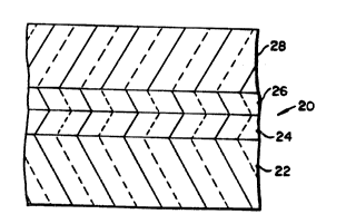
Referring to FIG. 2, a four layer waveguide
structure 20 includes a substrate 22, a waveguide film
24 formed on the substrate 22, an overlay material 26
positioned on the waveguide film 24, and a cladding
material 28 positioned on the overlay ma~erial 26. The
refractive index of the substrate 22 is less than the
refractive index of the waveguide film 24, and the
refractive index of the waveguide film 24 is less than
the refractive index of the overlay material 26. The
refractive index of the cladding material 28 is less
than the refractive index of the overlay material 26,
and the refractive index of the cladding material 28 is
less than or equal to the refractive index of the
substrate 24. The cladding material 28 is positioned
on the overlay material 26 and waveguide film 24 and
has a lower refractive index than the waveguide film 24
and overlay 26.
Referring to FIG 3, a drawing of light guided
in a slab waveguide, such as devices 10 or 20, is
shown. The ray trace represents the propagation of a
wavefront totally internally reflected at the film
boundaries. The propagation of electromagnetic energy
is characterized by a projected wave vector, ~, on the
z-axis and is def~ned
~m = (2~/~)*(nwsin~m) (1)
where ~, is the wavelength of light, nw is the
waveguide refractive index, and ~ is the propagation
20~ ~30
angle. For a waveguide system, defined by the
refractive indices and the thicknesses of the layers
and the wavelength and polarization of light, discrete
values of ~ are allowed and termed the propagation
modes indicated by m. These values are derived by the
phase effects of boundary conditions at the film
interfaces and the round-trip propagation distance of a
reflection cycle within a waveguide having a refractive
index nw.
The effective refractive index, Nw, of a
waveguide assembly is the ratio of the velocity of
light in vacuo to that in the waveguide. Creating
patterned regions of differing N is the basis of
constructing devices to perform geometrical optics.
NWm is defined by the propagation angle ~ specific to a
mode m and waveguide refractive index nw where
NWm = nwsin~m (2)
The Nwm value impacts the propagation of light in the
two dimensions within the plane of a slab waveguide
just as the real refractive index affects the
propagation of light in the three dimensions of bulk
material.
When multiple modes are excited within a
waveguide, beam steering or focusing properties can
vary significantly if the film assembly is not designed
properly. This is a major concern if there is an
optical axis along which there are additional devices
having dimensions about the size of the beam.
In the examples that follow, devices were
designed to refract light at the device boundaries
while eliminating modal dispersion by having the angle
of refraction the same for all modes of propagation.
The devices 20 were created by the addition of an
overlay material 26, having a higher index, to form a
208~ ~Q
device pattern on a waveguide 24 of lower index. The
device design is optimized for a specific waveguide
thickness and the existing modes therein by selecting a
corresponding overlay thickness where the ratio of the
waveguide N, NWm~ and the overlay N, Ndm, is nearly
equivalent for all modes existing within the waveguide
Nd0/Nw0 = Nd1/Nwl = Nd2/Nw2 = . . . Ndm/Nwm (3)
This ratio is termed the normalized N in the discussion
and figures below and is useful for considering the
refracting power of any single device.
In the first example, initially, the three
layer model 10 was used to calculate the Nw that
results for the light contained within the waveguide
14. The wavelength used was 830 nm, and the thin film
assembly is shown in FIG. 1. The waveguide 14,
nw=1.482, was prepared on a substrate 12 of silicon
dioxide, ns=l.453. These materials could represent the
assembly formed by flame hydrolysis. The thickness
dispersion of Nw was calculated for the seven modes ~nd
is presented in FIG. 4 where nw=l.544. Next, Nd was
calculated for the four layer assembly 20 of FIG. 2
where nO1=1.544. Setting the waveguide thickness to 10
~m and calculating the thickness dispersion of Nd
produces the results of FIG. 5. Only the first seven
modes are shown although additional modes could exist.
Finally, a search for the condition of E~. 3 over the
range of thickness values of the overlay 26 was
completed and an 11.05 ~m thick overlay film was found
to provide the least modal dispersion. The normalized
N values, having a standard deviation of 1.9 x 10⁻⁴
from the mean value, are plotted in FIG. 6.
As the refractive index of the waveguide 24
approaches that of the overlay film 26, the functions
describing the thickness dispersion for each mode of
2 0 ~
the three layer and four layer assemblies become more
similar. Finally, they reach the limit of being
identical and the four layer system would be analyzed
as a three layer system. Realistically however, a
difference in indices is required to simultaneously
meet the condition of Eq. 3 and maintain the basis of
device operation; that is, Ndm is not equal to Nwm-
With these principles in mind, the assembly 20 with the
least variation of the normalized N should be an
assembly 20 where the waveguide index has about the
same difference in value to the index of the overlay 26
as to the index of the substrate 22.
In the second example, this concept is
demonstrated again using the film assembly of FIGS. 1
and 2. The N dispersion of the three and four layer
assemblies are shown in FIGS. 7 and 8, respectively. A
waveguide where nw=1.544 and having a selected
thickness of 5 ~m supported six modes of propagation.
The overlay where nOl=1.6 had a thickness of 4.71 ~m
for the least modal dispersion.
For both examples, the deviation from the
mean values is a demonstration of the design of a
system having reduced modal dispersion. The second
example demonstrates an improved situation over that of
the first example in that the refractive index of the
waveguide is more near the average of ns and nOl. When
fewer modes are considered, the deviation of normalized
N values will also be smaller and the thickness of the
overlay will differ to reduce the deviation, especially
for the cases of the first example.
It will now be appreciated that the present
invention is a waveguide assembly fabricated in
accordance with design rules herein described that
control the sensitivity of waveguide device performance
to the presence of multiple modes of propagation. With
the present invention, it is possible to dramatically
2 ~ 3 ~
reduce the modal dispersion for all the modes supported
by the waveguide or to create the specific dispersion
desired for separation of light based on its mode of
propagation.
The construction of the four layer waveguide
assembly 20 has assumed the addition of the overlay 26
to an existing waveguide 24. It should be understood
that it is possible to also invert the order of the
waveguide layer 24 and overlay layer 26 in the
fabrication process and still create a mode insensitive
device.
While the invention has been described with
particular reference to the preferred embodiments, it
will be understood by those skilled in the art that
various changes may be made and equivalents may be
substituted for elements of the preferred embodiment
without departing from the invention. In addition,
many modifications may be made to adapt a particular
situation and material to a teaching of the invention
without departing from the essential teachings of the
present invention.
It can be appreciated that a method has also
been presented for fabricating a waveguide structure
having a substrate with a refractive index, ns~ and a
waveguide film with a refractive index, nw, formed on
the substrate. The method comprises the steps of
selecting a substrate having a refractive index, ns;
forming on the base a waveguide film having a
refractive index, nw, with nw being larger than nS; and
forming on the waveguide film overlay material having a
refractive index, nOl, with nOl being larger than nw.
As is evident from the foregoing description,
certain aspects of the invention are not limited to the
particular details of the examples illustrated, and it
is therefore contemplated that other modifications and
applications will occur to those skilled in the art.
2~g~
It is accordingly intended that the claims shall cover
all such modifications and applications as do not
depart from the true spirit and scope of the invention.