Note: Descriptions are shown in the official language in which they were submitted.
2~7~
MULTI-MODE INPUT/OUTPUT CIRCUIT AND MODULE. AND
PROCESS CONTROL SYSTEM USING SAME
FIELD OF THE INVENTION
This invention relates to input/output (I/O) circuits for
receiving signals from process-variable sensors and processing
them for delivery to a computer, and for receiving control
signals ~rom the computer for transmission to remote
controlled devices.
BACKGROUND OF T~IE INVENTION
Process control systems are known in which a plurality of
sensors sense one or more process variables to produce signals
which are transmitted to one or more controller computers; the
one or more controller computers normally control one or more
remote controlled devices which determine the value of the
process variable in accordance with the sensed value of the
variable, for example to hold it constant or to change it to
some new desired value.
As examples, the sensed process variable may be a fluid
flow rate, a temperature, a differential pressure, etc. and is
sensed by a sensor transducer which converts the value of the
process variable into an electrical signal which is supplied
to a transmitter for transmission to the one or more
controller computers. The controlled devices may be such
things as valves for controlling fluid flow, h~aters for
controlling temperature, devices for starting or controlling
the speeds of motors, etc.
It is common in such systems to provide I/O circuits
which are supplied with analog signals from the sensing
devices and which convert them to the desired digital form for
use by the one or more controller computers; it is also known
to provide I/O circuits which are supplied with digital
signals from the one or more controller computers and convert
, - :.
,
2~847~
them into analo~ signals for transmission to the controlled
devices.
Typically, each I/O circuit is connected to a pair of
terminals from which a two-wire line extends to a remote
transmitter or controlled devices, and contains appropriate
analog-to-digital and digital-to-analog circuits for producing
the desired interfacing between the transmitters and
controlled devices on one hand and the one or more controller
computers on the other hand. Thus each such pair of terminals
is normally associated with an I/O channel which receives
analog signals from the sensors to produce digital signals for
supply to the one or more controller computers, or which
receives digital data signals from a central controller
computer and supplies corresponding analog control signals to
the controlled devices. The first of this class of signals,
received from the sensors, may be described as input currents
or input voltages, depending on the nature of the sensor and
transmitter, and the second class of signals, which are
supplied to the controlled devices, may be described as output
currents or voltages.
The format of the signals from the transmitters may also
be differen~ in different situations; in the most common form
of system, the signals may be simple analog current levels or
voltages, but in some cases may comprise pulses the frequency
or sequence of which conveys the sensed information.
In general, the types of I/O circuits required to provide
these various functions in response to the several types of
signals are mutually exclusive in form, and a specific form of
I/O circuit must be used for each function. For example, a
current-input I/O circuit is different from a current-output
I10 circuit, and voltage-input and voltage-output I/O circuits
also differ each from the others.
- .
"` 2~8~76~
In this connection it is noted that "current input" and
"current output" do not necsssarily mean that the source of
the current is on one side or the other of the I/O terminal.
In general, both "2-wire" current input and "2-wire" current
output modes utilize a volta~e source in the I/O circuit to
provide the operating current; a current input mode is one in
which the current varies in accordance with the sensed process
variable, while the current output mode is one in which the
current sent out to a controlled device is determined by the
I/O circuit. In so-called "4-wire" current input, the
operating supply power is provided external to the I/O
circuit.
Several significant practical difficulties arise when
each of the I/O circuits is suited for only one particular
mode of operation, for example either current input, current
output, voltage input, voltage output or other. This is
primarily because the I/O circuits or channels are typically
bought and sold in groups or modulPs; that is, a unitary
module will typically have eight or sixteen pairs of
terminals, with the same type of I/O circuit associated with
each pair of terminals. Accordingly, each I/O module
comprises either a set of current input channels, or a set of
current output channels, or a set of some other type of
channel.
This presents a number of practical drawbacks. First,
unless thP number of I/O circuits of a given class needed by
the user happens to be just the number which is provided by
one or more modules, there will be at least some I/O circuits
which are unused, representing wasted space and money.
Further, each module typically handles only one type of signal
to or from a number of different remote points, so that the
different signals to and from any given plant area, for
example, will be distributed among several different modules;
this is often an inconvenience in servicing.
~:
2~7~
Large control systems are frequently assembled in the
manufacturer's factory, to the specifications of the customer,
then shipped to the customer's plant for installation. This
installation involves connections to a power source and
connections to field wiring. To protect delicate internal
circuitry and wiring, only the terminals for connection to the
field devices are accessible in the area in which the
installation connections are made.
All the signals to and from a given area of the plant are
frequently run in multi-conductor cables, trays, or conduits.
To facilitate wiring connections to the cables, trays, or
conduits, it is important that all the I/0 circuit connections
for a given cable or conduit be in close proximity. In the
past, this has led to the regrouping of connections to and
from I/O modules into new groups of terminals for installation
connections, located in additional cabinets, added for the
purpose. This practice is called "marshalling". An added
benefit of adjacency of connections for given areas of the
plant is easier maintenance, diagnosis, and repair.
U.S. Patent No. 4,593,380 of Mark J. Kocher et al, issued
June 3, 1986 describes a system employing I/0 circuits each of
which is selectively operable in different modes, either as an
input I/O circuit or as an output I/O circuit for exchanging
signals between a central processing unit of a controller and
a process being controlled. Such an I/O circuit, when
installed in plural form in a module along with other similar
circuits, enables the user to provide, in effect, any desired
combination of input and/or output I/0 circuits in that module
by appropriate programmed control of the individual I/O
circuits, as desired for purposes such as those mentioned
above.
The I/0 circuit of the '380 patent requires three I/O
terminals, a first of which is a common in/out terminal used
to connect to a lead extending to one side of a load device or
':
2a~
of an input device, whichever is to be used. In operating a
load device, the other side of the load is connected to a
second of the I/O terminals, which is supplied from one pole
of the operating power supply; when used to receive input
signals, the other side of the input device is connected to
the third I/O terminal, which is supplied from the other pole
of the operating power supply.
The circuit disclosed in the above-identified '380 patent
utilizes an IGT (Insulated Gate Transistor) connected between
the common in/out terminal and one side of the supply source,
and a preload resistor connected between the common in/out
terminal and the opposite power supply terminal. The IGT is
gated off when the circuit is operated as an input point, and
is switched on and off when the circuit is used as an output
point. The programmed controller is programmed to switch the
mode in which each I/O circuit operates in accord with whether
it is being used as an input or an output circuit. In this
way the same physical I/O circuit can be used for all of the
I/O circuits; one need only connect the external input device
or load device to the appropriate terminals and switch the
circuit to the appropriate mode by means of the programmed
computer.
It is an object of the present invention to provide a new
and useful I/0 circuit and module for use in a process control
system.
Another object is to provide such circuit and system
which does not require marshalling of leads.
Still another object is to provide such a new and useful
I/O circuit which can accommodate and handle analog current
and voltage inputs or outputs, as well as pulse signals or
other types of process control signals.
, . . .
.. : . ,,
,
,
2a8~7~
A further object is to provide such a circuit, and a
module employing same, which is inexpensive in the components
which it uses, and which lends itself especially well to
embodiment in an integrated circuit, at least in part.
Still another object is to provide such a circuit which
has provision for redundant operation of two identical
circuits, by paralleling I/O terminals of two "redundant
mates", one online, the other off-line, in a stand-by
~ondition.
A further object is to provide such a circuit which can
easily be modified to provide extremely reliable limltation of
voltages and currents applied to field wiring so as to avoid
causing explosions by sparks between the field wiring, or by
thermal heating of devices connected to the field wiring.
An additional object is to provide such a circuit in
which voltage signals representing the I/O current and the
input voltage, as well as voltage signals used to regulate the
output, are all referenced to the same power supply terminal.
It is also an object to provide such a circuit and system
in which each I/O channel is galvanically isolated from all
others, has excellent stability and reliability, and is
inexpensive and easy to service.
SUMMARY OF_THE INVENTION
These and other objects and features of the invention are
achieved by the provision o~ a new and useful I/O circuit
which is adapted to be electrically switched into any one of a
plurality of different modes in which it provides
corresponding different functions and operations, for example
so that the same I/O circuit may be electrically controlled to
handle analog input currents, analog output currents, analog
input voltages, analog output voltages, pulse current or
--6--
:: ~
, : . .,
~: , . - .~ .,
,
,, .
2~8~7~
voltage inputs or pulse current or voltage outputs, as
examples, as determined by electrical commands supplied
thereto.
The present invention provides a new and useful form of
multi-mode I/0 circuit, dif~ering from that o~ the '380 patent
in significant ways and having certain advantages in various
applications thereo~. In the I/0 circuit o~ the present
invention, there are employed a pair of I/0 terminals in
series combination with a load means and with an eleatrically
variable resistance device, across which series combination a
DC supply voltage is supplied. When a two-wire analog
current-input remote device is used, it is connected between
the above-mentioned two terminals, the variable resistance
device is automatically placed in its low resistance condition
by a programmed computer, and output is taken across the load
means serving as a current sensing element. When analog
current output signals are to be provided, the output leads of
the I/0 circuit extending to the remote controlled device are
connected to the pair of I/O terminals, and the variable
resistance device is modulated in resistance so as to vary the
output current in a predetermined manner, again upon
electronic command from an associated microprocessor. The
variable resistance device is preferably controlled by a
feedback circuit which minimizes the error between the actual
output current, as sensed by the voltage across the load
means, and the desired current commanded by the programmed
computer, via a digital-to-analog converter. This use of
feedback provides greater stability and reduced sensitivity to
changes in the value of the field load. Two-wire current
pulse inputs are handled in the same general way as the above-
described analog current inputs.
To provide output voltages to a high-impedance remote
load from the I/O circuit, an additional low resistance is
preferably connected between the two terminals, in parallel
with the remote load. In the voltage output mode, the circuit
, ., : :, : -~ ,
: -, : :
" ,1 , '
' ' . ,, :
7 ~ ~
functions just as in the current output mode. The output
current through the additional low resistance produces a
voltage proportional to the current. Provided that the value
of the additional low resistance is much less than the remote
load impedance, the ratio between output voltage and output
current is determined by the value of the additional low
resistance.
Designating the I/O terminal connected to the power
supply as the power terminal and the I/O terminal connected to
the variable resistance device as the common terminal, when
receiving a voltage input from a remote device the variable
resistance device is put into a low resistance condition and
the voltage signal source is connected between the common
terminal and a third voltage-input terminal, here designated
as the V-IN terminal. The V-IN terminal is in this case
utilized directly as the input to the I/O circuitry.
Connection is made through the variable resistance device and
load means, rather than a direct connection to the 0.0 volt
point of the I/O ¢ircuit, to reduce the number of terminals,
to permit disabling the circuit in the event of a malfunction
in a redundant system, and to minimize potential damage due to
miswiring the I/O terminals. The circuit which senses and
converts the voltage input draws very little current from the
voltage signal source; therefore, the series connection of the
voltage signal source with the variable resistance device and
the load means causes no significant change in the voltage
sensed and converted. This preferred circuit arrangement
provides a voltage signal, current sense signal, and variable
resistance device control signal, all referenced to the same
supply voltage terminal. This simplifies the design of the
integrated circuit or other related circuitry used in the I/O
circuit.
Voltage pulse inputs are handled in the same general way
as analog voltage inputs.
--8--
. .
, .
....
:, ,
, :
7 ~ 0
The mode in which each I/O circuit operates is preferably
controlled electrically from the one or more controller
computers by way of a microprocessor in each module, and can
be changed at any time, independently of the mode in which
other I/O circuits of the same module are operated.
Preferably each I/O circuit is galvanically isolated from
all others, that is, their DC supply voltage levels are
aompletely independent of each other and from system ground~
This channel-to-channel isolation permits the I/O channels to
be operated completely independently of each other, and
simplifies wiring considerations when connecting I/O circuits
to various devices. It also permits interconnection of
multiple I/O circuits in various ways, described below, to
accommodate even more signal types.
Other devices may be used in the I/O circuits for
auxiliary functions, or to provide safety features, and other
modes of operation including operation with bipolar input and
output signals are possible. Some of th~se modes involve a
combination of multiple interconnected I/O circuits for one
input or output signal.
There has therefore been provided a new and useful I/O
circuit and module in which each I/O circuit is independently
controllable electronically to change the mode in which it
operates to accommodate a variety of different input and
output conditions, with the various features and advantages
described above.
BRIEF DESCRIPTION OF FIGURES
These and other objects and features of the invention
will be more readily understood from a consideration of the
following detailed description, taken with the accompanying
drawings, in which:
. ,
2~7~
Figure 1 is a block diagram illustrating an over-all
system in which the invention is useful;
Figure 2 is a block diagram showing a preferred
embodiment of an I/O module according to the invention;
Figure 3 is a schematic diagram, largely in block form,
showing a preferred embodiment of the integrated circuit
(ASIC) used in the module of Fig. 2;
Figure 3A shows the status of the ASIC of Fig. 3 when
used to respond to analog current inputs;
Figure 3B shows the status of the ASIC of Fig. 3 when
used to produce analog current outputs;
Figure 3C shows the status o~ the ASIC of Fig. 3 when
used to respond to analog voltage inputs;
Figure 3D shows the status of the ASIC of Fig. 3 when
used to produce analog voltage outputs;
Figure 3E shows the status of the ASIC of Fig. 3 when
used to respond to pulse current inputs;
Figure 3F shows the status of the ASIC of Fig.3 when used
to respond to pulse voltage inputs;
Figure 3G shows the status of the ASIC of Fig. 3 when
used to respond to four-wire analog current inputs;
Figure 3H shows the status of the ASIC of Fig. 3 when
used to respond to four-wire pulse current inputs;
Figure 3I shows the status of the ASIC of Fig. 3 when
used to provide discrete DC output signals;
--10--
.; . . . . .
.. . - : : ~ ::.: :
,, :::,. :.: :
' ,"'", : : : ' :'
7 ~ ~
Figure 3J shows the status of the ASIC of Fig. 3 when
used to respond to discrete (on-off) DC swit~hed input
signals, for fast response;
Figure 4 is a block diagram illustrating how two I/O
channels of the invention may be combined to accommodate a
bipolar voltage input;
Figure 5 is a block diagram illustrating how two I/O
channels of the invention may he combined to produce a bipolar
output signal.
Figure 6 is a block diagram illustrating how two I/O
channels of the invention may be used to accommodate a bipolar
current input;
Figure 7 is a block diagram illustrating how two I/O
channels of the invention may be combined to produce a bipolar
output voltage.
Figure 8 is a schematic diagram, largely in block form,
of another embodiment of the invention, preferred when a
simpler system capable of fewer but important functions is
desired; and
Figures ~-11 are electrical schematic diagrams
illustrating certain ancillary features which preferably, but
optionally, are included in the system of Fig. 3.
DETAIL~D DESCRIPTION OF PREFERRED EMBODIMENTS
Referring now to the embodiments of the inv~ntion shown
in the drawings by way of example only, and without thereby in
any way limiting the scope of the invention, Figure 1 shows a
central control computer 10 which is to receive information
from, and transmit control signals to, various remote sensors
and controlled devices of a plant sub-system. In this example
, ~
. .;
- . ; ~ , . : .
.
2~7~
the sub-system consists of a temperature sensor 11 and a two-
wire analog current transmitter 12; a remotely-controlled
device 14 such as a valve positioner for controlling a valve
15; an analog voltage transmitter 16 responsive to a pH sensor
17 for sensing the pH of a liquid; a high input impedance
motor drive 18 controlled by an analog voltage supplied
thereto to operate a motor 19; a four-wire current transmitter
20 responsive to a fluid flow sensor 21; and, typically, other
sensors, transmitters, actuators and controlled devices (not
shown) all associated with a common su~-system, in one plant
area.
Also shown in Fig. 1 is a terminal strip 26 containing a
plurality of pairs of terminals such as 28a, 28c. Preferably,
in this example, each such pair of terminals is associated
with a third terminal such as 28b, to form triads of such
terminals. For convenience, only five such triads are shown;
a more typical number in practice, for this embodiment is
eight or sixteen. The remote devices, as shown, are connected
either to the upper and lower terminals of each triad or to
the center terminal and the lower terminal thereof.
In accordance with the invention a special multi-mode
plug-in I/O module 30 is electrically positioned between the
central control computer lO and the terminal strip 26. It
will be understood that in Figure 1 the various electrical
connecting lines shown may in fact each comprise many
conductors, line 32 for example constituting a system serial
data bus interconnecting the I/O module 30 and the central
computer 10, and line 34 representing a pair of leads
supplying an operating supply voltage of 24 volts DC, in this
example, from the central computer to the I/O module.
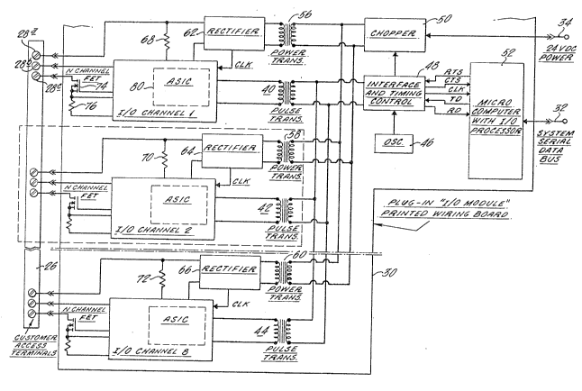
Turning now to Figure 2 depicting a single I/O module in
detail, for simplicity there are shown only three of the eight
triads of terminals on terminal strip 2~ of Fig. 1; the line
32 again represents the serial data bus to and from the
, -; ~, ~ . : ~
7 ~ ~
central station computer 10, and the line 34 applies 24 volt
D~ power to the I/O module 30. Also shown is a module
oscillator 46, an interface and timing control unit 48 and a
chopper 50 all for use in common by all the channels of the
module. A module microcomputer 52 containing a programmed I/o
processor is provided which controls operations in the I/O
module and communicates with the central station over bus 32.
Oscillator 46 provides the basic clock for the module. Pulse
transformers such as 40,42 and 44 supply signals between their
respective I/O channels and the interface and timing control
48. The details of how these elements cooperate in the module
will be described more fully below; suffice it here to note
that the chopper 50 chops the 24-volt DC power so that it can
pass through the isolating power transformers such as 56, 5
and 60 in Fig. 2 to the respective I/O channels. The power
transformers deliver the chopped supply voltage to
corresponding rectifiers such as 62, 64 and 66 respectively,
for each channel, which rectifiers in turn supply their output
DC through respective dropping resistors 68, 70 and 72 to the
circuits identified as I/O channel 1, I/O channel 2 and I/O
channel 8 in Fig. 2. Alternatively, a tap on the power
transformer can supply 12 volts DC directly to the I/O
channels.
It will be understood that the circuitry in the I/O
channels 1 through 8 ma~ be identical, and in this embodiment
are identical, with each other, hence only one channel
(channel 1) need be described in detail.
As shown in Figure 2, the positive voltage from rectifier
62 is supplied to terminal 28a of the terminal strip 26, and
the lower terminal 28c of the triad is connected through a
variable resistance device 74 and a load means 76 to local
ground, i.e. to the other, more negative side of the output of
the rectifier 62. The variable resistance device 74 is in
this example an N-channel field effect transistor (FET), and
the load device 76 is a low-valued fixed resistor.
-13-
:, .~ ,. . i . :
, ;': :
.
2~8~7~
Accordingly, it will be seen that the top and bottom I/O
terminals 28a and 28c are connected in series with the
variable resistance device 74 and with the load resistor 76,
across which series combination the isolated DC power supply
voltage is applied. As discussed previously, a two-wire
process-control transmitter or actuator may be connected
between terminals 28a and 28c, or a process-control voltage
transmitter may be connected between terminals 28b and
terminal 28c. For convenience and conciseness in
nomenclature, terminal 28a may be termed the "power" terminal
(to which the DC supply voltage is applied), terminal 28c the
"common" terminal since it is used for all input and output
signals, and terminal 28b the V-IN terminal. Under the
control of an application specific integrated circuit (ASIC)
~0 in each channel, the FET 74 is operated in its highly
conductive, low-resistance state or in a varying resistance
state, to produce the operations mentioned above and described
in detail hereinafter. In a preferred embodiment, the FET may
be a Motorola type MTD3055EL.
Referring to the more detailed diagram of Figure 3,
channel 1 of the module of Fig~ 2 is shown in detail,
corresponding parts being indicated by corresponding numerals
and the ASIC 80 being shown within the broken-line outline.
Here again are shown the power transformer 56, the
rectifier 62, the clock pick-off 86, the dropping resistor 68
which drops the 24 volts to 12 volts for use in the ASIC
circuitry, the application of the 24 volts to the power
terminal 28a of the I/O channel, and the connection of the
common terminal 28c through the MOSFET device 74 and the low-
valued resistor 76 (250 ohms typical) to local ground (0.0
v . ) .
The ASIC is designed to operate from a supply voltage of
approximately 12 volts; as mentioned above, this voltage may
be generated from an external supply, such as a center-tap on
-14-
. ~ ~ '
2~7~
the 24 volt power transformer secondary, or as shown it may be
derived from the 24 volt DC supply by means of the dropping
resistor 68 and shunt voltage regulator 100. In either case,
the 12 volts is applied to a voltage divider 90, with taps at
0.5 volts, 1.4 volts, 2.5 volts, 6.0 volts, and 12.0 volts.
The 12.0 Volt and 0.0 Volt taps supply power to the various
amplifying and sw.itching circuits within the ASIC. The 0.5
Volt tap is used to set a switching threshold for a comparator
140. The 1.4 volts and 2.5 volts, via switch S5, set a
switching threshold for comparator 120. The 6.0 volts is a
convenient bias voltage for proper operation of amplifier 9~.
If the internal shunt regulator is not used, the supply
voltage of 12 volts is applied only to the voltage divider
terminal, and no connection is made to the shunt regulator.
A filter capacitor 104 is connected across the 2~ Volt
supply, and another external filter capacitor 105 is connected
across the voltage divider within the ASIC. These capacitors
minimize the effects of rapid supply voltage fluctuations upon
the functioning of the ItO circuit.
The digital address of the channel is determined by the
jumpering of three address inputs designated A0, A1 and A2;
each may be jumpered to a DC supply point at 0 volts or to a
DC supply point at 12 volts, thus providing combinations of
jumper settings corresponding to binary numbers from 0 to 7.
These numbers are utilized to identify channels one to eight -~`
in the module (assuming an 8-channel module) for addressing by
the module microcomputer 52. Other than the setting of the
address jumpers, the same circuitry is used in all of the
ASIC's for all of the channels. The operating mode of each
channel is controlled by the states of five solid state
switches S1 through S5, which are controlled by the message
sent to that channel by the module computer 52.
More particularly, the data from the module computer 52
which passes through pulse transformer 40 is then passed
-15-
" . , ~
'' ,
2 ~
through a circuit comprising a differential line driver 72 and
a differential line receiver 73. Signals from the
differential line receiver are supplie~ to synchronous data
receiver/transmitter 78, to which the local address of the
channel is also supplied from the jumper address inputs A0, Al
and A2. In this connection it is noted that while most of the
lines in Fig. 3 are again shown in single-line form, each may
comprise many individual lines, as shown by a cylindrical
section about the line and a numeral adjacent the line, in
parenthesis, indicating the actual number of wires in that
line.
The specifi¢ ASIC shown in Fig. 3 is designed to operate
with currents at the I/O terminals 28a, 28c of 0-20 mA or 4-20
mA, and typically with input voltages at V-IN of 0-5 volts.
Output volta~e ranges can be controlled by the value of
external resistance. Typically, this range is 0-5 volts, but
it can be as large as 0-19 volts. The basic elements of this
ASIC are as follows.
The lines between the synchronous data
receiver/transmitter 78 and the differential line driver 72
and differential line receiver 73 are labelled "td" for
"transmit data", "rd" for "receive data" and "t/r" for
transmit/receive selection. Data are transmitted to the
computer 52 on td, and received from the computer on rd, while
the line t/r controls whether the line driver or the line
receiver is operative at any time. Switch S4 is labeled as a
"MUX" (multiplexer), and is in effect a 24-pole double-throw
solid-state switch.
The junction of resistor 76 with MOSFET 74 is connectable
through switch S3 to the analog-to-digital converter 85 (ADC),
the output of which is applicable to switching MUX S4 to the
synchronous data receiver/transmitter 78, and thence by way of
the td line through differential line driver 72 and pulse
transformer 40 to the module computer 52. In this way the
-16-
2~7~
analog current through resistor 76 is measured and converted
to an analog voltage, which is in turn converted to a
combination o~ digital binary signals, sometimes called a
code, and supplied as serial binary pulses to the module
computer 52 as desired. This path is shown by the hatched
lines in Figure 3A; note that in this mode of handling analog
current inputs, input switch S1 is connected to the 12 volt DC
supply to maintain the MOSFET in its highly conductive
condition, so it presents only a few tenths o~ an ohm of
resistance. Although the signal also follows other paths,
such as to "open" comparator 140 and to ~'pulse" comparator
120, the signals at the ends of these paths are not ultimately
used in the mode shown.
The switch conditions for the analog current output mode
are shown in Figure 3B for supplying an analog control current
to a remote controlled device, wherein the differential line
receiver 73 supplies digital data representing the current to
be transmitted, which is passed through the digital-to-analog
~DAC) converter 92 for conversion to an analog signal; the
latter analog signal, as shown in Figure 3B, is compared in
unity gain amplifier 94 with the actual current which is ~;`
sensed by resistor 76 and fed back via switches S3 and S2.
The resultant error is amplified by op amp 98 or, if capacitor
102 is used, integrated by ths combination of op amp 98 and
capacitor 102. The 6.0 volts supplied to 98 and 94 provides a
convenient bias voltage for proper operation of amplifier 98.
The output of amplifier 98 controls MOS FET 74 through switch
S1, so that the error between the desired current from DAC 92
and the actual current from 76 is brought essentially to zero.
Capacitor 102 is used to make amplifier 98 behave like an
integrator when it is necessary to filter out of the output
current noise which is present in the DAC output. Use of the
integrator can also improve stability of the output circuit.
In this example capacitor 102 is connected to terminals
available at the exterior of the ASIC due to the difficulty in
-17-
., ; , ,,
,
,,
.
.
:. ~ .
.
2~7~
fabricating within the ASIC a capacitor of the value required.
The capacitor value can be changed to vary the response speed
of the output circuit.
In the case of an analog voltage input supplied between
the V~IN and common terminals of the I/O circuit from a remote
voltage transmitter as shown in Figure 3C, the power terminal
28a is no longer connected to the external two-wire line. The
V-IN terminal 28B is connected through switch S3 to the ADC
85, the output of which is again supplied through the MUX
switch S4 to the s~nchronous data receiver/transmitter 78; the
digital data representing the voltage is thereby supplied to
the output line td for passage through the differential line
driver 72 to the module computer 52. Because the input to ADC
85 is a high impedance, almost no current flows through the
input circuit. Therefore, the "CO~" connection through FET 74
and resistor 76 causes almost no voltage drop, and thus, has
no detrimental effect on the converted signal.
These three modes of operation, namely current input,
current output and voltage input are the more commonly used of
the various modes of which the circuit is capable, the
current-input and current-output modes being by far the most
common. Thus, if desired, the V-IN terminal can be eliminated
and only the power and common terminals utilized while still
providing all of the modes of operation which do not require
use of the V-IN terminal.
Figure 3D shows the arrangement of the switches S1-S5,
and the addition of a low-valued resistor 110 between the
power and common terminals, as used in the analog voltage
output mode to supply a controlled analog voltage to a remote
high-impedance load indicated as 112. As in the case of the
analog current output mode, the command signal from the module
computer arrives over line rd, and the circuit switches are
set as for the current output mode. The principal difference
is that the low-valued shunt resistor 110 between the power
-18-
: . , -
,,
,,
: :
: :: : ::
: ~ .
2~7~
and common terminals produces a voltage drop, dependent upon
the output current. This voltage drop is supplied to the
remote high-impedance load. Because the shunt rasistance of
resistor llo is much lower in value than the remote high-
impedance load, the desired varying voltage will be supplied
to the remote load device despite variations in its impedance.
Also, if resistor 110 were not used, then the output current
required for reasonable output voltages would be too small for
adequate resolution of the signal.
Ths pulse current input mode is shown in Figure 3E, which
is the same as the analog current input mode of Figure 3A
except that multiplexer S4 now sends to thie synchronous data
receiver/ transmitter the data passing over a path extending
through S3, comparator 120, pulse counter and timer 122 and
line 124, in place of the data from the ADC 85. In this case,
each excursion of input current above 10 mA, corresponding to
the 2.5 volt threshold selected by S5, is counted and timed as
a pulse. This permits the computer to count pulses and
determine the pulse frequency and period.
Similarly, the pulse voltage input mode shown in Figure
3F is like that for the analog voltage input as shown in
Figure 3C, except that multiplexer S4 now sends to the
computer the data from the path extending through V-IN, S3,
comparator 120, pulse counter and timer 122 and line 124, in
place of the data from the ADC. In this case, each excursion
of input voltage above the threshold selected by S5, either
1.4 volts or 2.5 volts, is treated as a pulse. The threshold
is selected by the programmed computer to correspond with the
circuitry generating the pulses. Both thresholds are useful.
The computer uses the data from the pulse counter and timer to
count pulses and determine the pulse frequency and period.
The mode suitable for a four-wire analog current
input is shown in Figure 3G, and is the same as that for the
analog voltage input of Figure 3C, except that a low-valued
--19--
,. .
' ,
2~8~7~
resistor 123, for example of 250 ohms, is connected between
the V-IN and common terminals as shown. Resistor 123 converts
the externally-powered current signal into a voltage.
Fi~ure 3H shows the mode utilized for four-wire pulse
current input, which is like the pulse voltage input mode of
Figure 3F, except for the addition of the low-valued resistor
123 between the V-IN and common terminals.
Figure 3I shows a discrete, or on/off, DC output mode,
the switch S1 being shown in the "on" position. This mode can
be used, for example, to energize and deengergize a remote DC
relay. In this mode of operation, the received digital data
on line rd is supplied through the synchronous data
receiver/transmitter 78 to the mode control 81, signaling it
to switch Sl from its uppermost and downwardmost positions,
i.e. between the position in which the switch arm is supplied
with 12 volts to the position in which it is supplied with 0
volts; when connected to 12 volts, the MOSFET is "on" with
maximum current (lowest resistance), and when connected to 0
volts, it is off. This permits the MOSFET to be turned
completely on and off in accordance with commands from the
module computer to provide the desired output s.ignals to the
remote controlled devices.
There are a variety of other discrete, on/off, DC I/O
modes which can be provided b~ the circuits shown. For
example, Figure 3J shows the mode for a discrete on/off DC
switch input designed for fast response, the leads from the
remote on/off switch 130 being connected between the power and
common terminals and switch Sl being placed in its "full-on"
condition in which its arm is connected to the 12 volt supply.
Voltage from resistor 76 is applied to comparator 140 and
thence to synchronous data receiver/transmitter 78, to produce
on/off signals on the td line which are transmitted to the
module computer. As implemented in the preferred embodiment,
the signal from comparator 140 is always sent in all reply
-20-
- : - ,~ ,
.
, ~ ''.. :, . ,' ~ '
- , i ,, ,: ''- ~' :
~8~7~
messages from the I/O channel to the microcomputer, although
the microcomputer does not always use this information. In
the mode shown in Figure 3J, the data from the ADC are also
sent to the computer. However, the signal from comparator 140
will sometimes be preferred to the data from the ADC because
the comparator 140 can respond faster than the ~DC to changes
in switch state.
Some remote control devices and transmitters respond to
and/or generate serial digital data in the form of sequences
of pulses. Such sequences of pulses can be generated in the
I/O circuit, under control of the microprocessor, by changing
the position of Sl between the uppermost and downwardmost
positions, when the ASIC is configured as shown in Figure 3I.
These sequences can also be generated by changing the values
sent to the DAC, when the ASIC is configured as shown in
Figure 3B; in such case, capacitor 102 is preferably omitted.
Such sequences of pulses can be received and decoded by the
microprocessor, using the pattern of the ON/OFF signal from
the "open" comparator 140 when the ASIC iS configured as shown
in Figure 3J.
Process control equipment typically uses unipolar
signals, that is, signals which are always of the same
polarity or zero. These signals usually represent a process
variable which can change from 0 percent to 100 percent of
some full-scale value. The signal is usually scaled so that
the desired normal operating condition is near 50 percent of
the full-scale value. However some control systems,
particularly position or motion control systems, use bipolar
signals, that is, signals which may vary between positive and
negative polarities. Typically these signals are scaled so
that the desired normal operating condition is near the zero
value signal. To adapt a process control system which uses
the 0 to 100 percent representation of signals to handle
bipolar inputs and outputs, it is necessary to make t~e 50
percent representation correspond with the zero value input or
~ -21-
~% ~
output signal. This requires a shift in the zero value of
inputs and outputs.
Figures 4-7 show arrangements by which a bipolar voltage
input, varying for example ~rom -2.5 volts to +2.5 volts, or a
bipolar current, varying for example from -20 mA to +20 mA,
can be handled. In each case two channels of I/O are
utilized. Interconnectin~ channels to accommodate bipolar I/O
is possible because of the galvanic isolation between
channels.
In Fig. 4, channel 1 provides a constant 10 m~ output
current, which causes a voltage drop of 2.5 volts across the
250 ohm sense resistor 276 in channel 2. The connection of
pwr-to-com and com-to-pwr effectively produces a 48 volt
supply in series with the output of channel 1. The excess
voltage appears across channel l's output transistor, which is
rated to handle such voltage. Channel l's output transistor
is regulated by the channel 1 circuitry, to maintain an output
current of 10 mA, regardless of the output terminal voltage.
Channel 2's output transistor, on the other hand, is turned on
hard, and thus has a very low resistance. The 2.5 volt drop
across resistor 276 adds to the signal voltage from the
bipolar voltage source 200 twhich may be a tachometer) being
applied to the V-IN terminal of channel 2, so that an external
voltage signal of -2.5 volts appears to be 0.0 volts with
respect to channel 2's isolated 0.0 volt reference.
Therefore, an external voltage of -2.5 volts is converted by
channel 2 into a code which normally represents a voltage of 0
volts; an external voltage of 0 volts is converted by channel
2 into the code which normally represents 2.5 volts; and an
external voltage of ~2.5 volts is converted by channel 2 into
the code which normally represents 5.0 volts. Thus, the
current from channel 1 provides a bias which shifts the range
of input voltages converted by channel 2. The output signals
to the computer are supplied from channel 2 through pulse
transformer 235.
~22-
: . -:
.~ .
In Fig. 5, both channels are configured to produce output
current. However, channel 1 outputs current which is
proportional to the desired signal, and channel 2 output
current which is proportional to the full-scale output current
(20 mA) less the desired signal. Thus, when the desired
signal is at exactly mid-range, channel 1 outputs a current of
lO mA through the load 210 from top to bottom, and channel 2
outputs a current o~ 10 mA through the load from bottom to
top. The net sum of current is zero. This is equivalent to a
balanced, class--A, push-pull output circuit. If the desired
output signal is decreased to a value below mid-scale, channel
1 outputs less than 10 mA of current through the load from top
to bottom, and channel 2 outputs more than 10 mA through the
load from bottom to top. Thus, there is a net, non-zero
current through the load from bottom to top. For the maximum
desired signal, channel l outputs 20 mA, and channel 2 outputs
0.0 mA. Thus, the net current is 20 mA through the load from
top to bottom. For the minimum desired signal, channel 1
outputs o.0 mA, and channel 2 outputs 20 mA. Thus the net
current is 20 mA through the load from bottom to top.
In Fig. 6, an externally powered bipolar current source
220 produces a bipolar voltage across the external resistor
222 connected between the V-IN and Com terminals of channel 2.
The pair of interconnected channels then measures the voltage
as described for Figure 4. The external resistor's value is
selected so that full range of current from the bipolar
current source is converted to a voltage between -2.5 volts
and +2.5 volts. Output to the computer is then provided from
channel 2 by way of pulse transformer 237.
In Fig. 7, the two interconnected channels produce a
bipolar current output in load 225 just as in Figure 5.
Essentially all of this current flows through the external
resistor 226, and is thus converted to a bipolar voltage. The
resistor must be selected to convert a current between -20 mA
and +20 mA into the desired bipolar voltage range. The
-23-
.
2~8~6~
impedance of the "Hi-Z Load" must be significantly larger than
the external resistor's value, to retain accuracy.
The various circuit configurations of Figs. 4-7 are
readily provided by merely jumpering together certain of the
two triads of terminalsl and in some cases adding an external
resistor as shown.
Further with respect to preferred details of the I/O
module described above, the heart of the device is the
microcomputer 52, which may be a typ~ Motorola MC68302.
Besides a CPU memory and various computer I/O ports, this
device in this example contains an I/O communications
processor which is used to communicate with the rest of the
control system over the system serial data bus line 32 of Fig.
l, and to communicate with the I/0 channels through the
interface and timing control 48. Each I/0 channel receives
its power and timing information from the chopped 24 volts via
the power transformers. With such transformer coupliny of
supply power, and clock and data signals, each I/O channel is
galvanically isolated from every other channel.
To communicate with the I/O channels, the program in the
68302 directs the computer to send a message to a selected one
of the channels, which message contains the correct address
for the desired channel. Whenever an I/0 channel receives a
message addressed to it by the 6~302, that I/0 channel replies
with a message back to the 68302; as shown in Fig. 3, the five
lines shown between the 68302 and the interface and timing
control 48 are used to control the precise time a message is
sent, to time each bit of the message, and to convey the
transmitted and received data. In this connection, RTS means
request to send, CTS means clear to send, CLK means clock, TD
means ~ransmit data, and RD means receive data. Messages are
sent to each channel, and replies are received from each
channel, 180 times per second. Thus within 1 second, 1440
-24-
: - . ::, . ~.~. :. .
. ,- ~ . ,, , .,........ "
: ,. . :, ~ !
,: ' , : : , , ~ : :
2~7~
messages leave the 68302 and 1440 reply messages enter the
683 n~ .
With regard to the preferred message format, each message --
from the 68302 starts with a special pattern called a
"preamble". This is followed by the address of the channel to
be contacted, the desired mode of operation for the specified
channel, data for the D-to-A converter, and a "postamble"
which inaludes a CRC (cyclic redundancy check) error check and
a special end of message pattern. Each reply message follows
a similar format: preamble, channel address, status (which can
include various diagnostic signals as well as the output of
"open" comparator 140), either the A-to-D value or the pulse
count and timing values, and a postamble which includes a CRC
error check and a special end of message pattern.
For easy replacement, the I/O module plugs into a card
cage that contains the terminals for the field wiring.
Connectors in the I/O module connect to the power source and
system serial data bus, in addition to the field terminals.
The field wiring terminals are the only connections with the
I/O channel accessible to the customer.
The "open" signal from the comparator 140 near the top of
the ASIC unit is always sent in reply messages, as part of the
status indicating whether the I/O circuitry is functioning or
not. With 2-wire 4-20 mA signals, the "open" signal provides
a diagnostic signal when the current falls below 2 mA. This
is most likely caused by an open connection in field wiring.
This signal can also be used to monitor the state of a
discrete input. The status portion of the message can also be
used for various signals which permit the microcomputer to
verify that the circuit is working properly. For almost all
the configurations of the I/O circuit, portions of the
circuitry which are not essential for the given configuration
can be used to verify proper circuit operation. For example,
during the current output mode, the actual output current can
-25-
..:, , ~ ' ' ~ :" ',, ' `
:'
2~7~
be monitored by the ADC, and verified by the 68302 after each
reply message.
The N-channel enhancement mode output transistor, (an
inexpensive form of power metal-oxide semiconductor field
effect transistor) is arranged in a common-source
configuration with respect to the output, thus producing a
high-impedance current output which is ideal for 0-20 mA
outputs. The gate signal used to modulate the output
transistor 74 i5 also a relatively low voltage (e.g. 0 to
approximately 8 volts DC), referenced to the negative supply
output, the same reference as used for "current sense" and
"voltage sense" signals. The output transistor "looks like" a
common-drain circuit (a source follower which has close to
unity gain at lower fre~uencies) to the current regulating
feedback loop. This facilitates predictable stabilization of
the current regulating feedback loop and minimizes the effect
of the field load upon operation of the circuit. The use of a
MOSFET insures that the control signal to the output
transistor will not affect the D~ accuracy of the sensed
output current as would be the case with a conventional
bipolar junction transistor used in the same configuration.
When measuring voltage inputs in the embodiment described
above, a separate V-IN terminal is used so that the voltage
input circuit does not affect the accuracy of the current
sensing circuit, and to insure that, in case of malfunction or
improper configuration, power cannot be supplied into a low
impedance voltage transmitter output by the current output
circuit. The return connection for voltage inputs is made
through the common terminal. This does not introduce
significant error ~ecause the V-IN circuit is of very high
impedance (typically over one megohm) and draws almost no
current through the MOSFET and 250 ohm current sensing
resistor 76. The 250 ohm resistance in combination with the
isolation impedance, mostly capacitance, will limit the
maximum common mode rejection for voltage inputs. However,
-26-
-: :
: ~, . .
: .
.. - .
2~7~
the circuit performance is more than adequate with the 250 ohm
resistor in series with the return connection.
The current sensing, voltage sensing, and output FET
control signals are all referenced to the same terminal of the
power supply voltage. This permits the use of less expensive
and simpler single-ended (unbalanced) circuits in place of
balanced differential circuits. It is possible to arrange the
circuit this way because of the isolated power source.
The signal ranges for current sensing, voltage sensing
and output current control permit all of the circuitry to
operate on a supply voltage of 12 volts or less, even though
the field devices sometimes require higher voltages. Although
the voltage at terminal 28c can be expected to ~ary at times
throughout the range of 0.0 volts to 2~.0 volts, the signals
at 28 b, at point 84, and at the output of S1 to the gate 100
of output FET 74 all remain at lower voltages, usually 8 volts
or less, with most of the excess I/O terminal voltage being
dropped across the output FET 74. This lower supply voltage
requirement permits incorporation of almost all of the
circuitry into an inexpensive CMOS integrated circuit.
The 1.5 volt offset shown at 280, which is derived from
the power supply and switched into the output FET control loop
involving amplifiers 94 and 98, approximates the turn-on
voltage required by the output FET. Including this offset
voltage when the output control loop is not being closed
through the output FET minimizes the disturbance when the
output control loop is first switched into a mode which does
make amplifiers 94 and 98 control the output FET. This is
important when capacitor 102 is used to make amplifier 98 act
like an integrator, slowing the response of the output control
loop.
Another embodiment preferred for certain purposes is
shown in Figure 8. It offers only some of the features of the
-27-
- ~ .. . - ,. , . .~ , - . .
. : . .
2~
version described above, but at reduced cost. This embodiment
has no voltage input terminal, and has no isolation between
the channels. It also has no provision for counting pulses or
measuring pulse frequency. The circuit does provide isolation
between all the channels, as a group, and ground, and it does
provide basic "2-wire" current input and current output, as
well as voltage output when used with an external resistor.
The circuit is simple enough that no custom IC is necessary.
In this circuit, the nomenclature of "PWR" and "COM" for
the terminals is inappropriate, because the terminals formerly
called "PWR" terminals (28a) are all connected together
(suggesting a "common" I/O connection terminal). Also, the
terminals formerly called l'COM" (28c) are separate from each
other, and provide the signal output or signal input
connection for each signal. This change is necessary because,
without channel-to-channel isolation, some point in each
channel must be connected together. The I/O terminal which
connects to the power supply is the logical point to connect
the channels together.
Examining one of the I/O channels (e.g. channel 1 in Fig.
8), the circuit of current-sensing resistor 277, output
transistor 274, terminals 28c and 28a, and power source (-24
volts) are the same as with the previously shown embodiment,
except that the voltage polarities are changed. This polarity
change is necessary to conform with the industry convention of
having a negative polarity on the "common" terminal, in this
case 28a. The negative supply voltage is applied to terminal
28a, and the output transistor 274, connected between the
current sense resistor 276 and terminal 28c, is a P-channel
rather than an N-channel device. The per-channel control
circuitry is simpler, requiring onlv one op amp 286 per
channel. A single DAC 282 is shared among all channels by
means of a demultiplexing sample-and-hold circuit 285, which
periodically reads the DAC and, when the correct value for a
given channel is present, holds that value on the appropriate
-28-
2 ~
line until a new value is available. A single ADC 288 is
shared among all channels by an analog multiplexer 290, which
feeds a given channel's signal voltage to the ADC
periodically, at the correct times for the ADC to convert the
value and supply the converted digital code to the
microcomputer 300.
In a channel used for current output, the value sent to
the DAC 282, and held in the demultiplexing sample-and-hold
285, corresponds with the desired current. The op amp in each
channel regulates the resistance of the output transistor so
that the sensed current signal from resistor 277 balances out
the signal from the sample-and-hold. The two signals must be
of equal value with opposite polarity. The actual output
current can be monitored for diagnostic purposes by the signal
from sense resistor 277, which is fed through the multiplexer
290 to the ADC 288, and then, as a series of pulses, to the
microcomputer 300.
In a channel used for current input, the value sent to
the DAC 282 and held in the demultiplexing sample-and-hold 285
corresponds with the maximum allowed short-circuit current for
the I/0 circuit. In this case, the external device which is
regulating the current produces a current value less than the
short-circuit value. Therefore, the op amp circuit 286
saturates, turning on the output transistor 274 hard, so that
it has a very low resistance. The value of the current input
signal is represented by the voltage developed across the
sense resistor 277. This voltage signal is fed through the
multiplexer 290 to the ADC 288, and then to the microcomputer
300 as a series of pulses.
For voltage-output operation, an external resistor is
attached between terminals 28a and 28c. The circuit then
operates as for current output. The output current through
the external resistor produces the desired output voltage
signal.
, ~.
2~847~
Signals passing from the microcomputer 300 to the
isolated group o~ channels are optically isolated by isolator
304. The signal from the ADC,namely "DATA IN rd" is passed to
the microcomputer by way of optical isolator 305. The lines
from t~e isolator carry serial data from the ADC (labeled
"data in rd"), serial data to the DAC and channel select
circuit 320 (labeled "data out td"), a data clock for timing
serial data bits (labeled "data clk"), a continuous clock for
the ADC (labeled "adc clock"), and select lines for the ADC
288 ("adc sel"), the DAC ("dac sel"), and the channel select
circuit ("decoder sel") a total of seven signals. In
addition, there is an eighth line used as a secondary method
of disabling the off-line channels in redundant system.
While not shown in the Figures discussed in detail above,
various subsidiary circuit elements may be used in certain
preferred embodiments for increased safety, control or
monitoring. Typical arrangements employing such devices are
shown in Figs. 9-11. These figures show additional parts
included in the preferred embodiments to provide a secondary
means of disabling channels for redundant systems, to protect
the circuit from voltage spikes caused by interrupting the
current through inductive loads or by coupling of transient
disturbances from other wiring into the I/O circuit, and to
minimize circuit damage resulting from miswiring the terminals
to some external power sources. Other similar protective
circuits can be used, as well.
In the preferred embodiment first described above, with
channel-to-channel isolation and voltage inputs, an opto-
coupler 400 (Fig. 9) is preferably added to each I/O channel
in series with the supply voltage as a means of interrupting
the current to terminal 28a. This provides a second way to
disable the channel if the output transistor becomes shorted
in redundant systems, and it becomes necessary to disable the
channel. Diodes 402, 404 and 406, may be used to provide a
path for current flow from an inductance being switched off
-30-
;
:: ; . , ::
.: ~
2~
quickly. Diode 404 and resistors 410, 412 and 414 will
minimize damage from miswiring the terminals to some external
power sources. Resistor 412 can also reduce the amount of
high-frequency noise reaching the field wiring terminals.
In the alternative preferred embodiment of Fig. 8, which
does not provide channel-to-channel isolation and does not
handle voltage inputs, diode 428 (see Fig. 10) is preferably
used to provide a path for current from an inductance being
switched off quickly; diode 430 protects against miswiring to
some external power sources, and minimizes the chance that one
module of a redundant pair will affect operation of its mate.
Resistor 436 reduces the amount of high frequency noise
reaching the field wiring terminals, and minimizes damage from
miswiring the terminals to some. external power sources. Power
transistor 450 (Fig. 11) provides a second way to disable a
channel in Fig. 8 if any of the output transistors becomes
conductive due to various possible circuit failures, by
opening the series connection of the isolated 24 volt supply
to the load resistor 277 (Fig. 8).
It will be understood that the computer apparatus for
controlling the modes of the I/O circuit and for computing
output values need not be lumped in one or more controller
computers, but may be distributed in different locations as is
convenient for the particular application.
While the invention has been described with particular
reference to specific embodiments in the interest of complete
definiteness, it will be understood that it may be embodied in
a variety of forms diverse from those specifically shown and
described, without departing from the spirit and scope of the
invention.
-31-
. . , :
,' ' ' ~ '