Note: Descriptions are shown in the official language in which they were submitted.
WO91/20073 PCr/US91/03708
2~523~
--1--
MULTIPLE BUFFER COMPUTER DISPLAY CONTROLLER
APPARATUS
Back~round of the Invention
Resolution of each screen view of a computer
display sys~em is a ~unction o~ two components. One
component is the computer software which is executed
by the computer and which outputs signals for the
screen view. The other component is the monitor or
display unit itself which receives the screen view
signals from the computer. Typically a display
controller is used to hold screen view signals ~ ;
output from the computer and to reformat and
transmit the signals in a timely manner to
continually refresh the display unit screen. :
lS With the various software programs and monitors
available today, different combinations of software,
display controllers and display units are made.
Where the software requires for its output a certain ~;
pixel resolution of the receiving screen (monitor)
and thè monitor has`a larger pixel resolution,
correction is needed. Additionally, it is often
useful to be able to display very high resolution
continuous tone images on a monitor, but such high
resolution for displaying graphics on the same
monitor is unnecessary. This is especially the case
where a high resolution image display unit, for
example a typical l9 inch screen of 2560 pixels by -
2048 pixels, he~ce 200 DPI (dots per inch), and PC
software, which typically requires a receiving
.. ..
,, ~:
..
W09l/2~073
Ycr/us~)1/0370s
,_
2~8~2~5~
-2-
screen pixel resolution of 75-100 DPI, are utilized
together to display graphics (i.e. user editorial
marking~ and text) overlays on grey scale or color
images.
Another problem involves the demands placed on
the display controller. The memory in the display ;~
controller must not only continuously refresh the
monitor screen but also musk have suf~icient
band~idth so that new data can be loaded into the `~
memory quickly. One solution is to employ a video-
random-access-memory (VRAM) in the display
controller in a wide-word dual-ported configuration.
The VRAM has a memory matrix for holding data
(screen view signals) and a cooperating high speed
serial interface which transfers a multiplicity of
pixel data at a time and frees the memory for access
while simultaneously transmitting screen view
signals. The VRAMs however are expensive. ;~
Accordingly, there is a need for a computer
display system that provides high resolution image
display in an inexpensive, and diverse software and
hardware compatible manner.
~, .
Summary_ f the Invention -
The present invention provides computer display
controller apparatus which overcomes the problems of
prior art. The apparatus includes a display
controller coupled to the digital processor of a I `
computer system to receive therefrom display data-
corresponding to elements to be-displayed at
.. . - ~-' ' ''
`''
, , ,
WO~l/20073 PCT/US91/03~08
2~8~233
.
different respective resolutions. The display
~ontroller has a first memory for holding display
data corresponding ~o elements to be displayed at a
certain resolution and a second or additional memory
for holding display da~a corresponding to elements
to be displayed at other resolutions.
The display controller transfers, along one ~ ~-
channel to a data mixer, display data from the first
memory, and transfers along a separate channel
display data from the second memory. The data mixer
combines the display data ~rom the first and second,
and additional memories to form signals for dri~ing
a display unit coup~ed to the display controller.
Driving means drive the memories of the display
15 controller such that each pixel of display data from -
one of the first and second memories at one
resolution is replicated to fill several
corresponding pixels of the display unit of a higher
resolution. In turn, the data mixer signals drive
the display unit to display, at one resolution,
elements corresponding to the display data from the
first memory simultaneously with elements
corresponding to the display data from the second
memory at a different spatial resolution.
In a pre~erred embodiment, the first memory of
the display controller is a video RAM for holding
display data corresponding to graphics to be
displayed on the display unit. The graphics include
user generated markings and text. The second or
additional memories of the display controller are a
, ~ .
, ' - " ~ ~"":
WO91/20073 PCr/US9l/03708
2~8~233
--4--
plurality 4f DRAMs (Dynamic Random Access Memories)
for holding display data corresponding to images to
be displayed on the display unit. The images
usually are displayed at a higher resolution than
the graphics, the images and graphics being
displayed at the same time on the display unit with
the graphics usually overlapping the images.
To that ~nd, the present invention provides ~
display of elements corresponding to display data ;
from one of the first and second memories of the
display controller overlayed on elements ;
correspondin~ to display data Prom the other memory. ~ i
To accomplish this, the signals formed by the data
mixer include signals indicating precedence of ;~
settings of display unit pixels for the overlaying
elements over the settings of display unit pixels
for elements corresponding to display data from the
other memory. ~ `~;.s.
In accordance with another aspect of the
20 present invention, the data mixer forms signals as a ;
function of display data from one of the first and
second memories of the display controller.
In accordance with another feature of the
present invention, a transfer buffer is connected
between the digital processor and display controller
to hold display data until times of retrace of the ~ -~
display unit. During times of retrace of the
display unit, the transfer buffer transfers display i
data to the display controller. In a preferred
~ ~ ~ ~
' ~ ,':
:~ ,
::
.
,: :: ~:: :~ ., : : ::
WO9lJ20073 PCr/US91J03708
?$~233
embodiment, the ~ransfer buffer is a first-in
~irst-out buffer.
In a preferred embsdiment, a rectangle loader
is connected between the digital processor and the
display controller for providing indications of
memory ~ddresses for blocks of display data from the
digital processor to the display controller. The
rectangle loader enables transferring o~ display ,,
data from the transfer buffer to the display ; ',, '
10 controller in either a page mode or on a static '':~'
column cycle.
Further, the display unit may be operated in
either page mode or on a static column cycle with
signals from the data mixer ~o display the elements. ' ~ -
.: , . .
15 Brief Description of the Drawings ,'- ,
The foregoing and other ob~ects, features and
advantages of the invention will be apparent from '~
the following more particular description of '~;
preferred embodiments of the invention, as
20 illustrated in the accompanying drawings in which; ;'
like reference characters refer to the same parts ,
throughout the di~ferent views. The drawings are ,,~;
not necessarily to scale,,emphasis instead being ' ~'
placed upon illustrating the principles of the
25 invention. , ,~,,, ~ ;
-, Figure la.is a schematic illustration of an ;,~
image~plane and a graphics plane in a display system
of the,prese,nt invention.i, , j ,
,
!
WO g1t20073 PCr/USgl/03708
208~.33
-6-
Figure lb is a diagrammatic view showing
correspondence between positions on the graphics ;~
plane, image plane and screen view of Figure la.
Figure 2 is a block diagram o~ an embodiment of
5 the present invention.
,
Detailed Description of the Preferred Embodiment
The present invention provides for the high ;~
resolution display o~ an image on a monitor or
10 display unit 34 (Figure la~ of a computer system
simultaneously with the lower spatial resolution
display of graphics on the monitor screen. This is
accomplished by employing a high resolution image
plane 38 separate from a lower resolution graphic
15 plane 40 as illustrated in Figure la. The graphic
plane 40 is expanded and logically positioned in -- -
front of the image plane 38 such that graphics are ,
displayed overlayed on images in a screen view 36 of
the display unit 34.
By way of illustration and not limitation, the
screen view 36 is typically about 2.5 k pixels by 2 ;~ ~
k pixels. The image plane 38 is 2.5 k bits by 2 k ~ ~ -
bits by 8 bits deep to support 256 gray levels. The
graphic plane 40-is 1.25 k bits by 1 k bits by 2
25 bits deep to support a typical 100 DPI screen
resolution. The bits of the image plane 38 have a -~
one to one correspondence with the screen view 36
pixels, and the bits~of the graphics plane 40 have a
one to four correspondence with the screèn-view
30 pixels as illustrated in Figure lb. Thus, the
~,
- ~:
WO'.~ 0073 PCr/US~l/03708
2~ 233
shaded bit of the image plane 38 in Figure lb
denoted ~(xl,yl) positionally corresponds to the
screen view pixel indicated S(xl,yl). And in the
graphics plane ~0, the bit position labelled
G(xl,yl) positionally corresponds to screen view
pixels S(xl,yl), S(x2,yl), S(xl,y2) and S(x2,y2).
The other bits of the image plane 38 and graphics
plane 40 slimilarly corresponds to respective pixels
of the screen view 36.
Each screen view pixel is driven by signals
formed of the combination of the corresponding image
plane bit and graphics plane bit as follows. For
example, for each position in the image plane 38, an
8 bit signal is provided. For each position in the
15 graphics plan 40, a 2 bit signal is provided. The 8 ;
bit and 2 bit signals of a corresponding screen view
position are logically combined to provide an output ~ ,
value for driving the pixel of the screen view 36
position. ~he 8 bit image plane 38 signal and 2 bit ~;
qraphics plane 40 signal are preferably combined
according to the following table where Io.. I7 '
denotes the 8 bit signal of the image plane 38 and ~`
Go~ Gl ihdicates the 2 bit siqnal ~rom the graphics
plane 40.
~
., '~ . ' .
' ',~ ' :; : ~ "
. .
W09l/20073 PCT/US91/03708
r~
.
2 3 3
-8- : -
' ~ ', ,',
Table I
Image IN Graphics IN Output l,:,
1' Go , ' ; -~
,
I7.. .Io o 0 0 (black) ,,,~",- :, ,~,.
I7---10 , 0 1 127 (grey) '~
I7.. Io 1 0 I7.. Io ~tranSPare~t/ ;~: :
, , image)
I7.. ~Io 1 1 255 (white) - : '
10Thus, in ~he preferred embodiment, it is the 2 ' ' , :
bit signal from the graphics plane 40 which
determines the setting of screen view 36 pixels. If
the 2-bit graphics plane 40 signal is:00 indicating
a black bit positioned on the graphics plane 40, the
corresponding screen view pixel is set to 0 (black).
If the 2-bit graphics plane signal is 01 indicating
a gray level at the bit position in the graphics
plane 40, then an output signal for a gray level,
for example 127, is used to drive the corresponding :~:
20 screen view pixel. If the graphics plane 2-bit :~
signal is 10 indicating a bit position of the ~ 4
graphics plane 40 which is to give precedence to the
underlying image plane bit for that position, an
output signal indicating the image plane bits Io
through I7 for that position is used to drive the
,corresponding,screen view pixel. If the graphics
plane signal is a 11 indicating a white bit in the
graphics plane 40 then a white output value, for
. ~ . . ..
:
~: .
W09t/20073 ~'~r/US~l/0370#
2~85233
_9_
,,
example, gray level 255 is used to drive the
corxesponding screen view pixel. In this manner,
each screen view pixel is set so that the graphics
of the graphics plane 40 are displayed overlaying
the image of image plane 3~. -
~he foregoing is incorpora~ed in a display
system embodying the present invention as
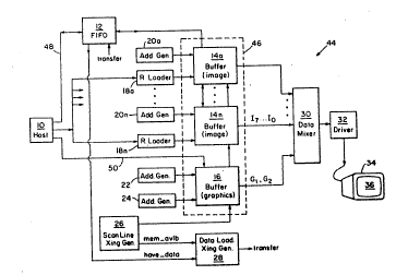
illustrated in Figure 2. The computer display
system 44 has a digital processor or host 10 which
generates output to be displayed on monitor 34.
Disital processor 10 may be a macrocomputer or a
minicomputer or of the PC type. Monitor 34 is any
video display or CRT common in the art, such as a
MegaScann UHR-2007. Host 10 transmits display data
on buses 48 and 50 to a multiple buffer dispIay `
controller 46. The display da~a includes image data
.
and graphics data. And buses 48, 50 are
bidirectional as described later.
Display controller 46 employs a plurality of
image buffers 14 for holding display data which -~
corresponds to images of an image plane 38 (Figures
la, lb). Display controller 46 also employs a
graphics bufPer 16 for holding display data
corresponding to graphics of a graphics plane 40
(Figures la, lb). Preferably, image buffers 14 are ~;~
dynamic RAMs each with at least 5 megabytes of
memory, such as a Motorola 514256 DRAM. And
graphics buffer 16 is a video RAM with at least one ;~
byte of memory, such as a Toshiba 524256 YRAM.
According to active scan line timing generator ~ -
,,
,
....... ~., '.' ~ .'
W091/20073 PCr/US91/03708
2~2~ 1
--1 o--
. .
26, 8-bit image signals ~I7... Io) are output from ~-
image buffers 14 and 2-bit graphics signals (GlGo)
are output from the graphics bu~fer 16 and are
multiplexed in data mixer 30. The clock rate of
timing generator 26 i~ coordinated with word width
of output from bu~fers l~, 16 to provide data mixer
30 with appropriate amounts of image data and , ,,
graphics data at a time. Address generators 20, 22 - ,,
of buffers 1~, 16 respectively are used to provide ~,
lO the proper memory address source of the image and ~ ,
graphi,cs signals being output at the clocking of
timing generator 26. The address generator 22 is of
the type capable of (i) repeating an address to ,~
replicate a pixel of a line on the same line such ' ,,
15 that two similar pixels are adjacent each other on , ,
the line and (ii) repeating addresses to replicate a -~
line of pixels to crea~e two identical adjacent rows ' ~,
of pixels. This provides the 1 to 4 correspondence '~
between graphics data of graphics plane 40 as held
in graphics buffer 16 and pixels of screen view 36.
,Each pixel GoG1 from the graphics buffer 16 is
replicated to four pixels of the screen view. ; -' ',~
Preferably, address generators 20 and 22 are of ' '~'
the Xilinx XC3030 type. Active scan line timing
generator ~6 is, for exàmple, a Signetics PLlOH20V
or a similar type. ' , ',-
Data mixer 30 combines the 8-bit image signal
'(I7~Io) from one image'buffer 14 and 2-bit graphics
signal (Gi,- Go) from graphics buffer 16 which~
correspond to a common screen view pixel. Data
; ~ ,
WOgl/20073 PCr/US9l/03708
2~8~æ33
mixer 30 accomplishes the combining by logic gates
arranged to implemen~ Table I described above. The
resulting output signal from data mixer 30 is
transferred to a display driver 32 coupled to data
mixer 30. Display driver 32 employs a digital-to-
analog converter to convert the data mixer output
signal to a voltage signal ~or driving the
corresponding pixel of screen view 36.
In the preferred embodiment, data mixer 30
includes a programmable logic array, such as a
Signetics PLlOH20V, coupled to a shift register or
similar memory such as a Booktree BT424. ~nd
display driver 32 is a Megascan serializer Ser-2007m
or similar digital-to-analog converter.
The foregoing proced~re is per~ormed ~or each
pixel of screen view 36 such that display driver 32 ~ -
and display unit 34 scans and updates each line
troW) of pixels of the screen view to refresh the ~
screen view 36. ~;-
In the preferred embodiment, active scan line
timing generator 26 clocks the buffers 14 and 16 of
display controller 46 such that display data for
driving the screen view 36 is output during active
scan line times of display unit 34. During retrace
time of display unit 34 (i.e. retrace between lines
of pixels as well as from the last line of pixels
back to the first line of pixels in screen view 36),
a data loading timing generator 28 enables the
transfer of i~age data between host 10 and image
buffers 14. This is accomplished as follows.
W09i/20073 Pcr/ussl/o37os
2~8h233
-12-
,
During times of retrace, active scan line
timing generator 26 disables the outpu~ of image and
graphics data signals from the ~emories 14, 16 of
display controller 46 and transmits a signal
(mem avlb) indicating availability of the display
controller memories 14, 16 to data loading timing ~
generator 28. That signal is logically ANDed with a -
signal (have data) from a transfer buffer 12 which
indicates that image data from ~ither host 10 or'an ~ ;
image buffer 14 is currently being held in ~he
transfer buffer 12. For the case where the
resulting signal indicates that the display driver
32 is currently in a state of retrace (i.e. it is
currently retrace time) and that transfer buffer 12
is currently holding subject data, the data loading
timing generator 28 enables transfer buffer 12 to
trans~er the subject data to the desired destination
(i.e. either an image buffer 14 or host 10). Data'~
loading timing generator 28 is preferably a ' :''' `~
Signetics PLS105 programmable logic array programmed
to implement an AND gate and other logic. Other
state machines which produce the transfer signal,
upon the receipt of the mem avlb and have_data '''
signals together''are also suitable
In a preferred embodimen't, transfer buffer 12' ;~1
is a first-in first-out buffer of 1024 bytes of
memory, and bus 48 is a bidirectional 32 bit wide' ~:
bus. To that end, transfer buffer 12 transfers
image'datà from-host lO to'-an image buffer 14 or-~
3a ~ice versa during retrace tlmes of display unit-34.
'
, ~ ,
WO91/20073 PCT/US~1/0370~
,
2~383233
-13-
This allows time saving transfer of imags data
between display and other host applications.
Also, host 10 transmits display data
corresponding to graphics to buffer 16 over
bidirectional bus 50. Since buffer 16 is a VRAM,
host lO can get immediate acce~s to buffer 16 the
majority of the time. Host access address generator
24 provides host lO with the address of the
available memory space in buffer 16. And scan line
timing generator 26 mem_avlb signal enables host 10
to transmit display data.
For further efficiency in loading display data
into image buffers 14 of display controller 46, the
present invention employs rectangle loaders 18.
There is a different rectangle loader 18 for each
image buffer 14. To transfer a block of image data ~ -
to an image buffer 14, host 10 provides an
indication of the extent of the block of display
data. Preferably, an indication of the upper left
hand corner and lower right hand corner of the block
of image data is used. Upon the clocking of data
loading timing generator 28, rectangle loader 18
cooperates with buffer 12 to load the subject block
of image data into a corresponding image buffer 14
in a static column cycle or page mode as known in
the ar~. Briefly, these two modes allow, for each
row address, a series of column addresses and column
~trobes to load the block of data into image buffer `~
14. In turn, this reduces the loading time where a
row address does not have to be separately given for
each column address.
~' " , ' '
, ~,
', -,
` ' . ' " "~'. ;',' ' . " ' ' ' ,' '"' ' ' ,.:" ., :' ' ~ ' , . ' :: .: "' ' : ' ,' ' ' : ' ' , :`
W091/2~073 PCT/US91/03708
,~ .
2~8~233
-14-
In a preferred embodiment, rectangle loaders 18
are Xilinx XC3030 address generators. Other address
generators of a similar ~ype are suitable.
Also as is common in the art, ~he page mode or
static column cycle manner of displaying a block of
data on the monitor 34 may be employed by display
driver 32. Thus, efficiency is provided in both
loading of image data into image buffers 14 as well
as displaying image data on monitor 34.
While the invention has ~een particularly shown ~ ;
and described with reference to a preferred `
embodiment thereo~, it will be understood by those
sXilled in the art that various changes in form and
datails may be made therein without departing from
the spirit and scope of the invention as defined by
the appended claims. For example, the relative
resolution between graphics plane 40 and image plane
38 and, hence, displayed graphics and images may be
other than l to 4 described above for purposes of
illustration and not limitation.
: : ,
'"
- .
.. . ..