Note: Descriptions are shown in the official language in which they were submitted.
~ -1- 2085270
HIGH FREQUENCY ELECTRICAL CONNECTOR
Technical Eield
This invention relates to an electrical connector, and more particularly to
an electrical conneetor having reduced crosstalk between wire-pairs.
5 Back~round of the I~ n
Inform~tion flow has increased substantially in recent years, and
n~lwolh~ have evolved to accommodate not only a greater number of users but alsohigher data rates. An ç~mple of a relatively high speed network is the subject of
ANSI/IEEE Standard 802.5 which provides a description of the peer-to-peer protocol
10 procedures that are defined for the transfer of information and control between any
pair of Data Link Layer service access points on a 4 Mbit/s Local Area Network with
token ring access. At such data rates, however, wiring paths themselves become
~ntenn~e that both broadcast and receive electrom~n~tic radiation. This is a
problem that is aggravated when station haldwal~ requires multiple wire-pairs.
15 Signal coupling (crosstalk) between different pairs of wires is a source of
interference that degrades the ability to process incoming signals. This is manifested
qu~ntit~tively as decreased signal-to-noise ratio and, nltim~tely, as increased error
rate. Accordingly, crosstaLt~ becomes an increasingly significant concern in
electrical equipment design as the frequency of interfering signals is increased.
CrosstaLk occurs not only in the cables that carry the data signals over
long distances, but also in the connectors that are used to connect station hardware to
the cables. ANSI/IEEE St~ndard 802.5 discloses a Medium Tnterf~e Connector
having acceptable crosstaLlc rejection at the frequencies of interest. This Connector
features four signal contacts with a ground contact, and is hermaphroditic in design
25 so that two identic~l units will mate when oriented 180 degrees with respect to each
other. This Connector is available as IBM Part No. 8310574 or as Anixter Part No.
075849. CrosstaLk rejection appears to result from short connector paths, groundshields, and the selection of particular termin~ls for each wire-pair. As might be
expected, such connector arrangements are relatively expensive and represent a
30 dep~u,e from comm~lnic~tinn plugs and jacks such as specified in Subpart F of the
FCC Part 68.500 Registration Rules and used in telecommunication applications.
For reasons of economy, convenience and standardization, it is desirable
to extend the utility of the above-mentioned telecommunication plugs and jacks by
- - using them at higher and higher data rates. Unfortunately, such plugs and jacks
*
2085270
include up to eight wires that are close together and parallel - a condition that leads
to excessive crosstalk, even over relatively short dist~nces. Attempts to improve this
condition are compli~ted by the fact that an ~cignment of particular wire-pairs to
particular tPrmin~l~ already exists which is both standard and non-optimum. Indeed,
5 in ANSI/EIAmA-568 standard, the termin~l ~ssignment for wire-pair 1 is straddled
by the termin~ signmPnt for wire-pair 2 or 3. If the electrical conductor.~ thatinle~onllect with these termin~ are close together for any distance, as is the case in
present de~ign~, then crosstalk between these wire-pairs is particularly troublesome.
Accordingly, is is desirable to reduce crosstalk in electrical connectors such as the
10 plugs and jacks commonly used in telecommunication equipment.
S~ of the Invenffon
In accordance with the invention, an electrical connector for connecting
an ordered array of input tPrmin~ls to an ordered array of output tPrmin~ls is
pluvt;d. The connector includes at least four conductors that are spaced apart from
15 each other and make electrical interconnection between the input and output
termin~ The con(luctors are generally parallel to each other along a portion of the
inler~ollllection path and are arranged to change the relative ordering of termin~ls,
between input and output, from the ordering that would re~ult if all conductors were
confined to the same plane.
In an illnst~tive embodiment of the invention, the input termin~l~ of the
electrical connector comprise insulation-displacing connectors, each having a pair of
opposing contact fingers which functions to make electrical and mechanical
connection to an in.~ul~tPd wire inserted therein. Further, the output termin~l~ of the
electrical connector comprise wire sprin~s. Two lead frames, each compri.~ing an25 array of conductors, are mounted on a dielectric block. Each conductor termin~tPs,
at one end, in a wire spring and, at the other end, in an in.~nl~tion-displacingconnector. Selected conductors of the lead frames cross over each other when they
are mounted on the diPhPctric spring block, but are p~evellted from m~king electrical
contact with each other at the point of crossover -- one of the conductors incl~ldes an
30 upward reentrant bend and the other includes a dowllw~d reentrant bend.
Advantageously, the two lead frames are identi~l, but are reverse-mounted on thespring block in the left-to-right direction. The front side of the spring block includes
a projection which fits into one end of a jack frame and interlocks therewith.
Together, the spring block and jack frame comprise a standard modular jack of the
35 type specified in the FCC Registration Rules.
2085270
- 3 -
Brief Des~ ,lion of ~e D~
The invention and its mode of operation will be more clearly understood
from the following ~et~iled description when read with the appended drawing in
which:
5FIG. 1 discloses the use of a modular co~nector to interconnect high
speed station ha~d~ e with a com-ll~ ic~tioll cable;
FIG. 2 shows the jack contact wiring ~ssignmentc for an 8-posidon,
telecommunications outlet (T568B) as viewed from the front opening;
FIG. 3 is an exploded perspective view of a high frequency electrical
10 connector in accordance with the present invention;
FIG. 4 discloses a top view of the lead frame used in the present
invention and its associated carrier;
FIG. 5 discloses a side view of the lead frame and carrier of FIG.4;
FIG. 6 shows a top view of a portion of the spring block used in the
15 present invention illustrating the region where crossover of the lead frames takes
place;
FIG. 7 di~closes a partial cross section~l view of the spring block of
FIG. 6 in the region where crossover of the lead frames ta~es place;
FIG. 8 shows frequency plots of near end crosstalk between diLre~nl
20 wire-pairs of an electri~l connector;
FIG.9 shows frequency plots of near end crosstalk between diLrelelll
wire-pairs of the sarne electric~l connector used in FIG. 8 after improvement by the
teachings of the present invention; and
FIG.lOis a top view of the lead frames shown in FIG. 3, after
25 assembly, illu~lla~ g the crossover of certain conductors in region n.
Detailed D~ .lion
Most communication systems tr~n.~mit and receive electrical signals
over wire-pairs rather than individual wires. Indeed, an electrical voltage is
me~nin~l~oss without a reference voltage - a person can't even get shocked unless
30 part of his body is in contact witn a reference voltage. Accordingly, the use of a pair
of wires for electrical signal tr~n.~mi~.~ion is merely the practice of bringing along the
reference voltage rather than relying on a local, fixed reference such as earth ground.
Each wire in a wire-pair is capable of picking up electrical noise from noise sources
such as lightning, radio and TV stations. However, noise pickup is more likely from
35 nearby wires that run in the same general direction for long distances. This is known
- 208~270
as crosstalk. Nevertheless, so long as each wire picks up the same noise, the voltage
dirre,~llce between the wires remains the same and the dirrere,llial signal is
unaffected. To assist each wire in picking up the same noise, the practice of twisting
wire-pairs in various patterns emerged.
FIG. 1 disclosesan ~ olmectionbetweenhighspeedstation
hd~d.. alt; 200 and cable 70 which comprises a number of wire-pairs. Flectrical
interconnection between the station hardwd.e 200 and cable 70 is f~cilit~t~d by the
use of standard telecommunications connectors that are frequently referred to asmodular plugs and jacks. Specifications for such plugs and jacks can be found in10 Subpart F of the FCC Part 68.500 Registration Rules. Assembly 100 is adapted to
accommodate the use of modular plugs and jacks and comprises connector 30, jack
frame 20 and wall plate 10 which interlock together to provide a convel~ient
receptacle for receiving modular plug 50. Inserted into opening 25, on the front side
of jack frame 20, is the modular plug 50 which commnniC~tps electrical sign~l.c, via
15 cable 60, to and from station ha,.lw~ue 200. Inserted into the back side of jack
frame 20 is electri~l connector 30 which is constructed in accordance with the
principles of the invention. Wires from cable 70 are pressed into slots located on
opposite side walls of connector 30 and make mech~nir~l ,and electrical connection
thereto. Four identic~l slots (not shown) are symmetrically positioned on the
20 opposite side of connector 30. Wall plate 10 includes an opening 15 that receives
and interlocks with jack frame 20.
Terminal wiring ~si~nments for modular plugs 50 and jacks 20 are
specified in ANSI/ELA/TLA-568-1991 which is the Commercial Building
Telecommunications Wiring Standard. This Standard associates individual wire-
25 pairs with specific termin~ls for an 8-position, telecomm~lnications outlet (T568B) in
the manner shown by FIG. 2. The Standard even prescribes the color of each wire
and Near End CrosstaL~ perform~nce in the frequency range 1-16 MHz. While the
color a~i~nment does not lead to difficulties, the pair a~signment does - particularly
when high frequency signals are present on the wire-pairs. Consider, for example,
30 the fact that wire-pair 3 straddles wire-pair 1, as ill~lstrflted in FIG. 2, looking into
opening 25 of the jack frame 20. If the jack frame and connector 30 (see FIG. 1)include electrical paths that are parallel to each other and are in the same
appro~imate plane, there will be electrical crosstaLk between pairs 1 and 3. As it
turns out, many electric~l connectors that receive modular plugs are configured that
35 way, and although the amount of crosstalk between pairs 1 and 3 is in.cignificant in
2085270
the audio frequency band, it is unacceptably high at frequencies above 1 MHz. Still,
it is desirable to use modular plugs and jacks of this type at these higher frequencies
because of connection convenience and cost.
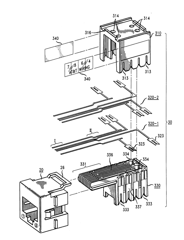
FIG. 3 discloses an exploded perspective view of high frequency
S electrical connector 30 and jack frame 20 showing their assembly in greater detail.
F1PCtr;Ca1 collnector 30 compri.~eS spring block 330, metallic lead frames 320-1,
320-2, cover 310, and labels 340 joined together as in(licat~Pd Referring briefly to
FIG. 4. Lead frame 320 comprises four flat, elongated conductive elements 322 that
te, at one end, in in~ul~tion-displacing connectors 323. Peripheral support
10 structure 321 holds the conductive elements in a fixed relationship with respect to
each other so that the lead frame can be easily handled; however, it is removed
during assembly. Lead frame 320 is shaped into a desired electrical interconnection
pattern which is, illnstr~tively, stamped from 0.015 inch metal stock and gold plated
in region I. During assembly, region I is bent around spring block 330 (see FIG. 3)
15 to become the spring contacts within a modular jack. Because a portion of the lead
frame is used as a spring contact, the entire lead frame itself is made from a resilient
metal such as beryllium-copper although a variety of metal alloys can be used with
similar results. Conductive e1emçnt~ 322 are parallel to ea,ch other and reside in the
same plane. In order to reduce crosstalk between conductive elçmçnts, a technique
20 is disclosed in which certain of the conductive elemçnt.c are made to cross over each
other in region II. Such crossover is not appa~n~ in FIG. 4, but can be clearly seen
in FIG. 3 where two idçnti~l lead frames 320-1, 320-2 are installed on top of each
other, but reversed from left-to-right. Each of these lead frames is identical to the
one shown in FIG. 4. Although a number of techniques can be used to electrically25 isolate the lead frames from each other, particularly in the region of the crossover,
the p~felled embodiment achieves electr1c~l isolation by introducing a re-entrant
bend in region II of the lead frame. This is most clearly seen in the side view of lead
frame 320 shown in FIG. 5. Thus, when a pair of lead frames 320 are reversed from
left-to-right and laid on top of each other, the conductive elements 322 bulge away
30 from each other in region II. Another way to achieve electrical isolation is to insert a
dielectric spacer, such as mylar, between the lead frames. Although this technique
avoids the need for a reentrant bend in the lead frame, an additional part is required.
FIG. 10 discloses a top view of a pair of lead frames after assembly in
accordance with the invention, illustrating the crossover of certain conductors in
35 region II. FIG. 10 is intended to clarify the way in which the conductors 322 of lead
208~270
frames 320-1 and 320-2 (see FIG. 3) cross over each other. The top lead frame
(~esign~ted 320-2 in FIG. 3) is shown with .~h~ing in FIG. 10, and the bottom lead
frame (de..~ign~ted 320-1 in FIG. 3) is shown without sh~ing in FIG. 10. Note that
there is no electrical coMection between any of the condllctors, particularly in region
S II where the crossover occurs; note also that the top and bottom lead frames are
identical to each other, but r,eversed from left to right.
The positioning of region II where the crossover occurs has been
empirically delermilled. Distance "d," indil ~ted in FIG. 5, is located at the
applo~llate midpoint of the signal path between the locations where electrical
10 coMections are made at the ends of the conductive paths. Since each conductive
path has a different length, different crossover points are required for optimumresults. Nevertheless, substantial crossta1k reduction is achieved in easy-to-
manufacture lead frame 320 where the entire lead frame is creased along a singleline.
Referring again to FIG. 3, lead frames 320-1, 320-2 are positioned on
the top surface 336 of spring block 330 which incl~l~es grooves having the same
pattern as the lead frame itself. Heat is, then, selectively applied to the grooves, via
ultrasonic welding, in order to deform the thermoplastic m,~tPri~l from which the
spring block is made to perm~nelltly join the lead frames and spring block together.
20 Insulation-displacing connectors 323 are folded down the sides of the spring block
while the conductors in region I of lead frames 320-1, 320-2 are wrapped around
tongue-like protrusion 331 of the spring block 330. Thereafter, cover 310 is joined
to the spring block to create a unitary structure. In the present embo~iiment~ spring
block 330, cover 310, and jack frame 20 are all made from a thermoplastic m~teri~
25 such as Polyvinyl Chloride (PVC).
After the insulation-displacing co~nectors 323 of the lead frame are
folded around each side wall 337 on opposite sides of the spring block, the spaces
between the opposing contact fingers that form the insulation-displacing connectors
are aligned with wire-receiving slots 333 of the spring block so that a wire may pass
30 therebelweell. Side walls 337 are subst~nti~lly parallel to each other and
perpendicular to the top surface 336 of the spring block. Furthermore, when
cover 310 is joined with spring block 330, its slots 313 are aligned with the spaces
between opposing contact fingers of the in~ tion-displacing connectors 323. As aresult, the insulation-~ispl~cing connectors are sandwiched between the spring block
35 and cover, and protected from the possibility of an inadvellenl electrical short
2~85270
-7 -
between adjacent connectors. After the cover is joined to the spring block, pins 334
in the spring block protrude through two of the holes 314 in the cover. These pins
are heated and deformed, via ultrasonic welding, to perm~nP.ntly join the cover to the
spring block. Cover 310 incl~ldes four symmetric~lly-po.~ition~d holes 314 so that it
5 can be interlocked-with the spring block in either of two positions. Electrical
connector 30 may now be inserted into jack frame 20 which incl~l~les latch 26 that
cooperates with shoulder 316, molded into the top of cover 310, to interlock the two
together. Note that jack frame 20 shows numbers 1 and 8 on its front face that
establish a numbering convelllion for the positioning of terminals within the jack
10 frame in acco~ance with option B of the ANSI/EIA/TL~-568 standard. Wiring
labels 340 also include numbers 1-8 that identify which slot 313 is interconnected to
each specific termin~l Such labeling is particularly useful in the present invention
where crossovers made by the conductors of lead frames 320-1, 320-2 change the
relative ordering of wires from the ordering that would result if all the conductors
15 were confined to the same plane.
I~.q.fçrring now to FIG. 6 there is provided a more detailed view of the
top surface 336 of spring block 330 in the region that is inserted into the jack frame.
In particular, the pattern of grooves in the top surface are spown in detail to
demonstrate the manner in which crossover between conductor paths is
20 accomplished. Grooves 332-1 ... 332-8, molded in the top surface 336, are
approximately 0.03 inches deep and 0.02 inches wide to accommodate a lead frame
which includes conductors whose cross-section is generally square (0.015 x 0.015inches) that are inserted therein. Dielectric walls sep~ale the grooves to provide
electrical isolation for the conductors of the lead frame. However, certain of the
25 dielectric walls, for e~mpltq. the wall between grooves 332-1 and 332-2, are
discontinuous in the region were crossover occurs. Furthermore, the grooves are,illustratively, 0.05 inches deeper in this region. This is shown in the FIG. 7 cross-
sectional view of the spring block. The purpose of the deeper groove is to
accommodate the reentrant bend in the lead frame where crossover occurs. By thus30 crossing over the condllctor~ of the lead frame, crosstalk between otherwise parallel
electrical paths is substantially reduced and the ability to use such
telecommunication jacks at higher frequencies is made possible. Indeed, crosstalk
reduction in the order of 15 dB is possible at the higher frequencies.
-8- XU85270
The improvement offered by the present invention is dr~m~tically
illustrated in the frequency plots of FIG. 8 and FIG. 9. FIG. 8 shows frequency plots
of near end crosstaik (NEXT) between different wire-pairs of the electrical connector
shown in FIG. 3 in which lead frames 320-1 and 320-2 are replaced with a single 8-
S conductor lead frame without crossovers. Frequency is plotted log~. ;L~ y in theho~i7O~ l direction as an exponent of the base 10. For example 1.00 corresponds to
101 = 10 MHz. At this frequency, the signal power co~ ic~ted to wire-pair 3
from wire-pair 1, de.ci~n~ted (1,3~, is 48 dB below the signal power on wire-pair 1.
As might be expected (1,3) = (3,1). The results at the far right-hand side of this
10 frequency plot show crosstalk between the various wire-pairs in the 16 MHz region
(i.e., 10l 25 MHz = 17.7 MHz).
FIG. 9 shows frequency plots of NEXT between dirfelent wire-pairs of
the electr~c~l connector shown in FIG. 8 where three crossovers are used in
accordance with the invention. A decrease in the amount of crosstalk between one15 set of wire-pairs often leads to an increase in the amount of crosstalk between
another set of wire-pairs. For example, the crosst~lk at 10 MHz bt;lween wire-pairs
(1,3) is 65 dB below the actual signal power which corresponds to an improvement,
when compared with FIG. 8, of 17 dB for wire-pairs (1,3);,however, crosstalk is
increased between wire pairs (1,4) by the present invention. Nevertheless, the net
20 effect is particularly desirable because the worst case crosstalk is so improved to the
degree that the subject telecommunications jack is now suitable for use in connection
with the IEEE 802.5 token ring.
Although a particular embodiment of the invention has been disclosed,
various modifications are possible within the spirit and scope of the invention. In
25 particular, it is understood that crossovers between dirrel~nl conductors will result in
dirÇel~ amounts of crosstalk between the different wire-pairs. As illustrated,
decreasing the amount of crosstalk between specific wire-pairs sometimes results in
increasing the amount of crosstalk between other wire pairs. Furthermore, cll~n~ing
the location where crossover takes place influences the amount of crosstalk. These
30 considerations are a matter of design choice. Crossover may be achieved using a
double-sided printed wiring board and the use of metal staples or plated-throughholes to achieve electric~l connection. Finally, the principles of the present
invention may be incorporated in numerous connectors including modular plugs andjacks as well as connecting blocks.