Some of the information on this Web page has been provided by external sources. The Government of Canada is not responsible for the accuracy, reliability or currency of the information supplied by external sources. Users wishing to rely upon this information should consult directly with the source of the information. Content provided by external sources is not subject to official languages, privacy and accessibility requirements.
Any discrepancies in the text and image of the Claims and Abstract are due to differing posting times. Text of the Claims and Abstract are posted:
| (12) Patent: | (11) CA 2085337 |
|---|---|
| (54) English Title: | BURIED-TYPE SEMICONDUCTOR LASER DEVICE |
| (54) French Title: | LASER A SEMICONDUCTEUR ENFOUI |
| Status: | Expired and beyond the Period of Reversal |
| (51) International Patent Classification (IPC): |
|
|---|---|
| (72) Inventors : |
|
| (73) Owners : |
|
| (71) Applicants : |
|
| (74) Agent: | SMART & BIGGAR LP |
| (74) Associate agent: | |
| (45) Issued: | 1998-10-20 |
| (22) Filed Date: | 1992-12-14 |
| (41) Open to Public Inspection: | 1993-06-19 |
| Examination requested: | 1995-12-08 |
| Availability of licence: | N/A |
| Dedicated to the Public: | N/A |
| (25) Language of filing: | English |
| Patent Cooperation Treaty (PCT): | No |
|---|
| (30) Application Priority Data: | ||||||
|---|---|---|---|---|---|---|
|
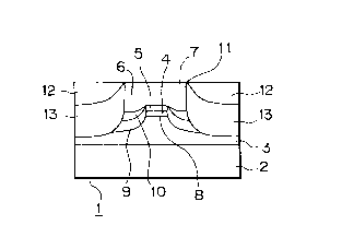
This invention provides a buried-type semiconductor laser device
that operates stably and reliably at a high temperature for a prolonged
period of time. A buried-type semiconductor laser device according to the
invention comprises a semiconductor substrate 2, a first ridge mesa 8 formed
on said substrate 2, said first ridge mesa 8 being covered on the top with at
least an active layer 4 and provided at both lateral edges with current
blocking layers 9, 10 of p-n reverse junction semiconductors arranged along
the active layer for confining electric currents, and a second ridge mesa 11
formed by said first ridge mesa 8 and said current blocking layers 9, 10 and
provided at both lateral edges with a semi-insulating layer 13.
Cette invention est un laser à semi-conducteur enfoui fonctionnant de façon stable et fiable à une température élevée durant une période de temps prolongée. Le laser de l'invention comprend un substrat semi-conducteur 2, un premier mésa à crête 8 formé sur ce substrat 2, ce premier mésa à crête 8 étant recouvert d'au moins une couche active 4 et portant sur ses deux bords latéraux les couches électriquement isolantes 9, 10 de jonctions p-n montées le long de la couche active pour confiner les courants électriques, et un second mésa à crête 11 formé par ce premier mésa à crête 8 et ces couches électriquement isolantes 9, 10 qui porte une couche semi-isolante 13 sur ses deux bords latéraux.
Note: Claims are shown in the official language in which they were submitted.
Note: Descriptions are shown in the official language in which they were submitted.
2024-08-01:As part of the Next Generation Patents (NGP) transition, the Canadian Patents Database (CPD) now contains a more detailed Event History, which replicates the Event Log of our new back-office solution.
Please note that "Inactive:" events refers to events no longer in use in our new back-office solution.
For a clearer understanding of the status of the application/patent presented on this page, the site Disclaimer , as well as the definitions for Patent , Event History , Maintenance Fee and Payment History should be consulted.
| Description | Date |
|---|---|
| Inactive: IPC deactivated | 2011-07-27 |
| Inactive: First IPC derived | 2006-03-11 |
| Inactive: IPC from MCD | 2006-03-11 |
| Inactive: IPC from MCD | 2006-03-11 |
| Time Limit for Reversal Expired | 2004-12-14 |
| Letter Sent | 2003-12-15 |
| Grant by Issuance | 1998-10-20 |
| Pre-grant | 1998-04-09 |
| Inactive: Final fee received | 1998-04-09 |
| Notice of Allowance is Issued | 1998-03-04 |
| Notice of Allowance is Issued | 1998-03-04 |
| Letter Sent | 1998-03-04 |
| Inactive: IPC removed | 1998-02-24 |
| Inactive: IPC assigned | 1998-02-24 |
| Inactive: IPC removed | 1998-02-24 |
| Inactive: First IPC assigned | 1998-02-24 |
| Inactive: IPC assigned | 1998-02-24 |
| Inactive: Approved for allowance (AFA) | 1998-02-23 |
| Inactive: Status info is complete as of Log entry date | 1997-10-10 |
| Inactive: Application prosecuted on TS as of Log entry date | 1997-10-10 |
| Request for Examination Requirements Determined Compliant | 1995-12-08 |
| All Requirements for Examination Determined Compliant | 1995-12-08 |
| Application Published (Open to Public Inspection) | 1993-06-19 |
There is no abandonment history.
The last payment was received on 1997-09-19
Note : If the full payment has not been received on or before the date indicated, a further fee may be required which may be one of the following
Patent fees are adjusted on the 1st of January every year. The amounts above are the current amounts if received by December 31 of the current year.
Please refer to the CIPO
Patent Fees
web page to see all current fee amounts.
| Fee Type | Anniversary Year | Due Date | Paid Date |
|---|---|---|---|
| Request for examination - standard | 1995-12-08 | ||
| MF (application, 5th anniv.) - standard | 05 | 1997-12-15 | 1997-09-19 |
| Final fee - standard | 1998-04-09 | ||
| MF (patent, 6th anniv.) - standard | 1998-12-14 | 1998-11-18 | |
| MF (patent, 7th anniv.) - standard | 1999-12-14 | 1999-11-17 | |
| MF (patent, 8th anniv.) - standard | 2000-12-14 | 2000-11-17 | |
| MF (patent, 9th anniv.) - standard | 2001-12-14 | 2001-11-19 | |
| MF (patent, 10th anniv.) - standard | 2002-12-16 | 2002-11-19 |
Note: Records showing the ownership history in alphabetical order.
| Current Owners on Record |
|---|
| THE FURUKAWA ELECTRIC CO., LTD. |
| Past Owners on Record |
|---|
| AKIHIKO KASUKAWA |
| TOSHIO KIKUTA |

