Sélection de la langue

Search

Sommaire du brevet 2085337 

Énoncé de désistement de responsabilité concernant l'information provenant de tiers

Une partie des informations de ce site Web a été fournie par des sources externes. Le gouvernement du Canada n'assume aucune responsabilité concernant la précision, l'actualité ou la fiabilité des informations fournies par les sources externes. Les utilisateurs qui désirent employer cette information devraient consulter directement la source des informations. Le contenu fourni par les sources externes n'est pas assujetti aux exigences sur les langues officielles, la protection des renseignements personnels et l'accessibilité.

Disponibilité de l'Abrégé et des Revendications

L'apparition de différences dans le texte et l'image des Revendications et de l'Abrégé dépend du moment auquel le document est publié. Les textes des Revendications et de l'Abrégé sont affichés :

  • lorsque la demande peut être examinée par le public;
  • lorsque le brevet est émis (délivrance).
(12) Brevet: (11) CA 2085337
(54) Titre français: LASER A SEMICONDUCTEUR ENFOUI
(54) Titre anglais: BURIED-TYPE SEMICONDUCTOR LASER DEVICE
Statut: Périmé et au-delà du délai pour l’annulation
Données bibliographiques
(51) Classification internationale des brevets (CIB):
  • H01S 05/227 (2006.01)
  • H01S 03/06 (2006.01)
  • H01S 05/323 (2006.01)
(72) Inventeurs :
  • KASUKAWA, AKIHIKO (Japon)
  • KIKUTA, TOSHIO (Japon)
(73) Titulaires :
  • THE FURUKAWA ELECTRIC CO., LTD.
(71) Demandeurs :
  • THE FURUKAWA ELECTRIC CO., LTD. (Japon)
(74) Agent: SMART & BIGGAR LP
(74) Co-agent:
(45) Délivré: 1998-10-20
(22) Date de dépôt: 1992-12-14
(41) Mise à la disponibilité du public: 1993-06-19
Requête d'examen: 1995-12-08
Licence disponible: S.O.
Cédé au domaine public: S.O.
(25) Langue des documents déposés: Anglais

Traité de coopération en matière de brevets (PCT): Non

(30) Données de priorité de la demande:
Numéro de la demande Pays / territoire Date
3-353614 (Japon) 1991-12-18

Abrégés

Abrégé français

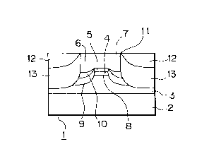
Cette invention est un laser à semi-conducteur enfoui fonctionnant de façon stable et fiable à une température élevée durant une période de temps prolongée. Le laser de l'invention comprend un substrat semi-conducteur 2, un premier mésa à crête 8 formé sur ce substrat 2, ce premier mésa à crête 8 étant recouvert d'au moins une couche active 4 et portant sur ses deux bords latéraux les couches électriquement isolantes 9, 10 de jonctions p-n montées le long de la couche active pour confiner les courants électriques, et un second mésa à crête 11 formé par ce premier mésa à crête 8 et ces couches électriquement isolantes 9, 10 qui porte une couche semi-isolante 13 sur ses deux bords latéraux.


Abrégé anglais


This invention provides a buried-type semiconductor laser device
that operates stably and reliably at a high temperature for a prolonged
period of time. A buried-type semiconductor laser device according to the
invention comprises a semiconductor substrate 2, a first ridge mesa 8 formed
on said substrate 2, said first ridge mesa 8 being covered on the top with at
least an active layer 4 and provided at both lateral edges with current
blocking layers 9, 10 of p-n reverse junction semiconductors arranged along
the active layer for confining electric currents, and a second ridge mesa 11
formed by said first ridge mesa 8 and said current blocking layers 9, 10 and
provided at both lateral edges with a semi-insulating layer 13.

Revendications

Note : Les revendications sont présentées dans la langue officielle dans laquelle elles ont été soumises.


THE EMBODIMENTS OF THE INVENTION IN WHICH AN EXCLUSIVE
PROPERTY OR PRIVILEGE IS CLAIMED ARE DEFINED AS FOLLOWS:
1. A buried-type semiconductor laser device comprising a
semiconductor substrate, a first ridge mesa formed on said substrate, said
first ridge mesa being covered on the top with an active layer and provided
at both lateral edges with current blocking layers of p-n reverse junction
semiconductors arranged along the active layer for confining injection
currents, and a second ridge mesa formed at least by said first ridge mesa
and said current blocking layers and provided at both lateral edges with a
semi-insulating layer.
2. A buried-type semiconductor laser device according to claim 1,
wherein said active layer has a bulk structure, a quantum well structure or a
strained quantum well structure.
3. A buried-type semiconductor laser device according to claim 1,
wherein said active layer formed on said first ridge mesa is covered with a
clad layer.
4. A buried-type semiconductor laser device according to claim 1,
wherein said second ridge mesa formed by said first ridge mesa and said
current blocking layers additionally comprise clad and contact layers.
5. A buried-type semiconductor laser device according to claim 1,
wherein said current blocking layers are made of n-InP and p-InP.
6. A buried-type semiconductor laser device according to claim 1,
wherein said semiinsulating layer is made of Fe-doped InP and covered with an
InP layer or polyimide.
7. A buried-type semiconductor laser device according to claim 5,

wherein an InP layer is formed on said semi-insulating layer.

Description

Note : Les descriptions sont présentées dans la langue officielle dans laquelle elles ont été soumises.


2~8~337
BURIEn- ~PE SEMICONI)IICTOR LASER DEVICE
B~CKGRnUND OF TUE INVENIION
[Field of the Invention]
This invention relates tn an improvement on a buried-tYpe
semiconductor laser device to be used as a light source in an optical
telecommunication system.
[Prior Art]
A semiconductor laser device to be used as a light source in an
optical telecommunication system is required to have various functional
features such as a high output power and a low threshold current, and a high
speed modulation capability.
A buried-type semiconductor laser device (having a BH structure) is
known to meet such requirements.
Fig. 2 of the accompanying drawings illustrates a typical known
buried-type semiconductor laser device.
Referring to Fig. 2, the buried-type semiconductor laser device 14
comprises an n-InP semiconductor substrate 15, on which an n-InP buffer laYer
16, a nondoped GaInAsP active layer 17 (having an energy band gap wavelength
of 1.3~ m), InP clad layers 18 and 19 and a GaInAs contact layer 20 are
sequentially formed by means of an epitaxial growth technique such as the
MOCVD method to bring forth a multilayer structure.
Additionally, p-InP current blocking layers 21 and n-InP current
blocking layers 22 extends from the respective upper edges of the clad layer
18 to cover the etclled areas of the buffer laYer 16 and then grooves 23 are
cut through the current blocking layers 21 and 22, the clad layer 19 and the

2085337
contact layer 20 in order to reduce the device capacity. The ~rooves 23 and
part of the segmented contact layer are covered by an SiOz insulating film 24
[Problem to be Solved by the Invention]
A buried-type semiconductor laser device 14 having a configuration
as illustrated in Fig. 2 is subiect to internal stresses (distortions)
particularly in the active layer 17 which is particularly remarkable at high
temperature due to the significant difference in the thermal expansion
coefficient between and the close physical proximity of the insulating films
24 covering the surface of the grooves 23 and the active layer 17.
A semiconductor laser device 14 which is subject to such
distortions cannot reliably operate for a long period of time.
[Object of the Invention]
In view of the above identified technological problem, it is
therefore an object of the present invention to provide a buried-type
semiconductor laser device that operates stably and reliablY at high
temperature for a prolonged period of time.
SU~MARY O~ THE INVENTION
According to the invention, the above object is achieved by
providing a buried-type semiconductor laser device comprising a semiconductor
substrate, a first ridge mesa formed on said substrate, said first ridge
mesa being covered on the top with at least an active laYer and provided at
both lateral edges with a current blocking layers of p-n reverse junction
semiconductors arranged along the active layer for confining electric
currents, and a second ridge mesa formed by said first ridge mesa and said
current blocking layers and provided at both lateral edges with a

2085337
semi-insulating laYer.
Said active layer preferably has a bulk struc-ture, a quantum well
structure or a strained quantum well structure.
Said active layer formed on said first ridge mesa is preferably
covered with a clad laYer.
Said second ridge mesa formed by said first ridge mesa and said
current blocking layers may additionally comprise clad and contact laYers.
Said current blocking layers may be made of n-InP and p-InP and
said semi-insulating layer may be made of Fe doped InP or polyimide and
covered with an InP layer.
[Function]
A buried-type semiconductor laser device according to the invention
can effectivelY confine injection currents by its current blocking layers of
p-n reverse junction semiconductors and therefore shows a low threshold
current for laser oscillation and a reduced capacity of the device due to the
arrangement of a semi-insulating layer.
More specifically, since a buried-type semiconductor laser device
according to the invention does not have grooves in the close proximity of an
active layer and insulating films covering the grooves (and having a thermal
expansion coefficient different from that of the active layer), it is
practically free from internal stresses and distortions even if it is driven
at a high temperature.
Thus, a buried-type semiconductor laser device according to the
invention operates stablY and reliablY for a prolonged period of time, if it
is driven at a high temperature.

208~337
BRIEF DESCRIPTION OF ~-IE D~AWINGS
Fig. 1 ;s a sectional view of a preferred embodiment of buried-type
semiconductor laser device of the invention.
Fig. 2 is a sectional view of a conven-tional buried-type
semicondllctor laser device.
DETAILED DESCRIPTION OF THE IN~ENTION
Now, the present invention will be described in greater detail by
referring to Fig. l of the accompanying drawings that illustrates a preferred
embodiment of the invention.
In Fig. l, the buried-type semiconductor laser device 1 comprises
an n-InP semiconductor substrate 2, on which an n-InP buffer layer 3, a
nondoped GaInAsP active layer having an energy band gap wavelength of 1.3
~m, a p-InP clad layer 5, a p-InP clad layer 6, a p-GaInAs contact layer 7,
a p-InP current blocking layer 9, an n-InP current blocking layer 10, an
n-InP layer 12 and a semi-insulating layer 13 are sequentially formed to
bring forth a multilayer structure and is provided with a first ridge mesa 8
and a second ridge mesa 11.
In a semiconductor laser device 1 having a configuration as
described above, the semiconductor substrate 2 tYpicallY may have a thickness
of 350m and the buffer layer 3, the active layer 4 and the clad layer 5 may
respectively have thicknesses of l~ m, 0.1~ m and 0.5 ~ m, while the clad
layer 6, the contact layer 7 and the current blocking layer 9 may
respectively have thicknesses of 2~ m, ~.3~ m and 2 ~m and the thicknesses
of the current blocking layer 10, the n-InP layer 12 and the semi-insulating
layer 13 maY respectively be 1 ~ m, 0.7~ m and 3 ~ m. although the above

2085337
figures are citecl nnLy as examples and the present invention is not limited
thereto.
The semi-insulating layer 13 maY alternatively he made of polyimide
and, while the active layer 4 of this embodimen-t has a bulk structure, it may
alternatively have a different structure such as a quantum well s-tructure or
a strained quantum well structure.
Since a semiconductor laser device 1 as described above is
subjected to current confinement to be realized by the current blocking
layers 9 and 10, involving a p-n reverse junction, it can be driven by a low
threshold current and the capacity of the device 1 is reduced by the
existence of segmented semi-insulating layer 13 disposed at the lateral sides
of the second ridge mesa 11.
What is more, the device 1 maintains its reliability because its
active layer 4 is practically free from stress, if the device 1 is used at a
high temperature for a prolong period of time.
The reason why the active layer 4 is immune to stress is that the
device 1 of the invention does not have any grooves which are covered by an
insulating film having a thermal expansion coefficient significantly
different from that of the active layer and located in the proximity of the
active layer as in the case of a conventional device described above by
referring to Fig. 2.
A buried-type semiconductor laser device 1 according to the
invention and illustrated in Fig. 1 can be prepared by way of a manufacturing
process as described below.
In the first step, a buffer layer 3, an active layer 4 and a clad

2085337
layer 5 are fornled on an n-InP semiconductor substrate 2 by a first
application of an epitaxi.al. growth technique (MOCVD method).
Then, in the second step, the surface of the clad layer 5 is masked
along a center line for a width of approximately 1.5~ m and the layers from
the clad layer 5 down to the buffer layer 3 are etched by a first application
of a (known) photolithography technique to produce a first ridge mesa 8.
Thereafter, in the third step, the surface of the active layer is
masked by SiOz and a current blocking layer 9 is formed in segments on the
areas that have been etched for the first time.
Then, segments of another current blocking layer 10 are selectively
made to grow on the respective segments of the current blocking layer 9 until
they reach the height of the surface of the active layer 4.
After removing the SiO2 mask, in the fourth step, a clad layer 6
and a contact layer 7 are sequentially formed on the active layer 4 and the
current blocking layer 10 by a second application of an epitaxial growth
technique.
Subsequently, in the fifth step, the surface of the contact layer 7
is masked along a center line for a width of approximately 5 to 20 ~ m and
then the layers from the contact layer 7 down to the buffer layer 3 are
etched by a second application of a Photolithography technique to produce a
second ridge mesa ll.
Then, in khe sixth step, a semi-insulating layer 13 and an InP
layer 12 are sequentially formed in segments on the second etched areas by
means of an epitaxial growth technique to produce a buried-type semiconductor
laser device 1.

2085337
Finally, in lhe seventh step, the SiO2 mask is removed from the
buried-type semicondllctor Laser clevice 1 ancl p- and n-electrodes are -formed.The above described sixth step may alternativelY be inserted after
the third step.
If the semi-insulating layer 13 is made of polyimide, the operation
of successively growing layers by means of an epitaxial growth technique will
be omitted.
[Advantage of the Invention]
As is apparent from the above description, a buried-type
semiconductor laser device according to the invention operates stably and
reliably at a high temperature for a prolonged period of time, because it is
free from distortions in its active layer due to stresses that may arise when
it is driven at a high temperature.

Dessin représentatif
Une figure unique qui représente un dessin illustrant l'invention.
États administratifs

2024-08-01 : Dans le cadre de la transition vers les Brevets de nouvelle génération (BNG), la base de données sur les brevets canadiens (BDBC) contient désormais un Historique d'événement plus détaillé, qui reproduit le Journal des événements de notre nouvelle solution interne.

Veuillez noter que les événements débutant par « Inactive : » se réfèrent à des événements qui ne sont plus utilisés dans notre nouvelle solution interne.

Pour une meilleure compréhension de l'état de la demande ou brevet qui figure sur cette page, la rubrique Mise en garde , et les descriptions de Brevet , Historique d'événement , Taxes périodiques et Historique des paiements devraient être consultées.

Historique d'événement

Description Date
Inactive : CIB désactivée 2011-07-27
Inactive : CIB dérivée en 1re pos. est < 2006-03-11
Inactive : CIB de MCD 2006-03-11
Le délai pour l'annulation est expiré 2004-12-14
Lettre envoyée 2003-12-15
Accordé par délivrance 1998-10-20
Préoctroi 1998-04-09
Inactive : Taxe finale reçue 1998-04-09
Un avis d'acceptation est envoyé 1998-03-04
Lettre envoyée 1998-03-04
Inactive : CIB enlevée 1998-02-24
Inactive : CIB attribuée 1998-02-24
Inactive : CIB enlevée 1998-02-24
Inactive : CIB en 1re position 1998-02-24
Inactive : CIB attribuée 1998-02-24
Inactive : Approuvée aux fins d'acceptation (AFA) 1998-02-23
Inactive : Renseign. sur l'état - Complets dès date d'ent. journ. 1997-10-10
Inactive : Dem. traitée sur TS dès date d'ent. journal 1997-10-10
Exigences pour une requête d'examen - jugée conforme 1995-12-08
Toutes les exigences pour l'examen - jugée conforme 1995-12-08
Demande publiée (accessible au public) 1993-06-19

Historique d'abandonnement

Il n'y a pas d'historique d'abandonnement

Taxes périodiques

Le dernier paiement a été reçu le 1997-09-19

Avis : Si le paiement en totalité n'a pas été reçu au plus tard à la date indiquée, une taxe supplémentaire peut être imposée, soit une des taxes suivantes :

  • taxe de rétablissement ;
  • taxe pour paiement en souffrance ; ou
  • taxe additionnelle pour le renversement d'une péremption réputée.

Les taxes sur les brevets sont ajustées au 1er janvier de chaque année. Les montants ci-dessus sont les montants actuels s'ils sont reçus au plus tard le 31 décembre de l'année en cours.
Veuillez vous référer à la page web des taxes sur les brevets de l'OPIC pour voir tous les montants actuels des taxes.

Historique des taxes

Type de taxes Anniversaire Échéance Date payée
Requête d'examen - générale 1995-12-08
TM (demande, 5e anniv.) - générale 05 1997-12-15 1997-09-19
Taxe finale - générale 1998-04-09
TM (brevet, 6e anniv.) - générale 1998-12-14 1998-11-18
TM (brevet, 7e anniv.) - générale 1999-12-14 1999-11-17
TM (brevet, 8e anniv.) - générale 2000-12-14 2000-11-17
TM (brevet, 9e anniv.) - générale 2001-12-14 2001-11-19
TM (brevet, 10e anniv.) - générale 2002-12-16 2002-11-19
Titulaires au dossier

Les titulaires actuels et antérieures au dossier sont affichés en ordre alphabétique.

Titulaires actuels au dossier
THE FURUKAWA ELECTRIC CO., LTD.
Titulaires antérieures au dossier
AKIHIKO KASUKAWA
TOSHIO KIKUTA
Les propriétaires antérieurs qui ne figurent pas dans la liste des « Propriétaires au dossier » apparaîtront dans d'autres documents au dossier.
Documents

Pour visionner les fichiers sélectionnés, entrer le code reCAPTCHA :


Pour visualiser une image, cliquer sur un lien dans la colonne description du document. Pour télécharger l'image (les images), cliquer l'une ou plusieurs cases à cocher dans la première colonne et ensuite cliquer sur le bouton "Télécharger sélection en format PDF (archive Zip)" ou le bouton "Télécharger sélection (en un fichier PDF fusionné)".

Liste des documents de brevet publiés et non publiés sur la BDBC .

Si vous avez des difficultés à accéder au contenu, veuillez communiquer avec le Centre de services à la clientèle au 1-866-997-1936, ou envoyer un courriel au Centre de service à la clientèle de l'OPIC.


Description du
Document 
Date
(aaaa-mm-jj) 
Nombre de pages   Taille de l'image (Ko) 
Abrégé 1994-03-31 1 16
Revendications 1994-03-31 2 36
Dessins 1994-03-31 2 14
Description 1994-03-31 7 201
Dessins 1996-10-20 2 15
Dessin représentatif 1998-09-10 1 3
Avis du commissaire - Demande jugée acceptable 1998-03-03 1 165
Avis concernant la taxe de maintien 2004-02-08 1 175
Taxes 1998-11-17 1 34
Correspondance 1993-04-06 3 52
Correspondance 1998-04-08 1 41
Taxes 1997-09-18 1 35
Taxes 1996-09-05 1 30
Taxes 1995-10-05 1 31
Taxes 1994-09-22 2 78
Taxes 1994-09-11 1 46