Note: Descriptions are shown in the official language in which they were submitted.
LOW VOLTAGE INHIBITING CIRCUIT FOR A MICROCOMPUTER
_a kqround of the Invent on
Field of the Invention
The present invention is directed to the field
5 of reset circuits for use with microcomputers and more
specifically to the area to reset circuits that provide
an inhibiting reset signal to a microcomputer when power
source voltage drops below a safe level.
Description of the Prior Art
It is well known that microcomputers operating
from regulated power ~upplies must ~e inhibited during
both the power-up phas~ and in the event that the DC
power to the regulated power supply is interrupted or
drops below a predetermined level.
Prior art circuits such as those shown in U.S.
Patent 4,367,423 provide complicated circuits that
generate reset signals for a micro~rocessor during the
time the circuit is initially powered up or when the
unregulated source ~oltage drops below a preselected
20 level. Generally such prior art circuits are expensive
and constitute a signi~icant ~rain on a battery source.
The primary objective of people working in this
area is to find a low cost solution to achieving the
desired ~unctions.
25 Summary o~ the Invention
The present invention is an improvement over the
prior art. It provides a low cost, low voltage detection
circuit with temperature stability and low power
consumption characteristics for use in conjunction with a
30 microcomputer. The circuit provides reset signals of at
' ' -
- 2 -
least a predetermined duration to the microcomputer
during power-up and in the event of a low voltagP
condition occurring in an associat~d DC power source.
During a low volta~e condition, the present invention
5 continues to apply the reset signal to the associated
microprocessor until the voltage is sufficiently low
enough that the microprocessor cannot attempt to operate
with such power applied. In addition, the present
invention has hysteresis characteristics of different
10 reset and nonreset threshold levels. In particular, a
first threshold level is defined as that which the power
source voltage must fall below in order for the circuit
to apply the reset signal from the microcomputer. A
second, slightly higher threshold level is defined as
15 that which the power source voltage needs to exceed in
order for the circuit to remove the reset signal from the
microcomputer.
It is an object of the present invent;on to
provide an improved circuit which minimizes the
20 electrical components necessary to provide low voltage
inhibiting of a microcomputer.
It is another object of the present invention to
provide a single circuit which has hysteresis
characteristics that are employed while monitoring
25 voltage of an associated power source and provides a
reset signal to a microcomputer having a duration that is
at least equal to a minimum predetermined time period.
It is a further object of the present invention
to provide a low voltage detection circuit that is
30 thermally compensated to maintain threshold stability
over a wide range of operating temperatures.
It is another object of the present invention to
provide a low voltage detection and reset circuit that
draws significantly less current than those known in the
35 prior art.
`~- 2~
-- 3 --
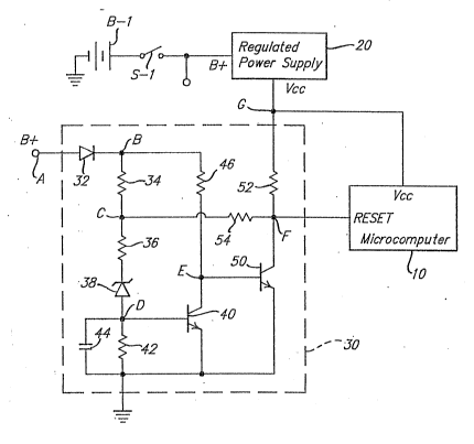
Brief DescriPtion of the Drawinq
The drawing is a schematic diagram of the
present invention.
Detailed Description of the Preferred Embodimen~
S In the drawing, a microcomputer 10 is shown
having a power input terminal Vcc that is connected to
receive a regulated voltage from a regulated power supply
20~ This embodiment~ as well as most applications in an
automotive vehicle electronics environment, requires the
10 value of Vcc to be 5.0 volts. The regulated power
supply 20 rsceives its unregulated B~ power from a
battery B-l. In the drawing, a switch S-l is shown to
symbolize the fact that the regulated power supply 20 can
be selectively energized by the battery B-l. In the
15 embodiment, the battery B-l is ideally charged to a
voltage of between 12 and 14 volts DC by a conventional
chargin~ device, such as, an alternator~regulator system
(not shown). Of course, other loads may be switchably
connected to the battery B-l by conventional switching
20 systems. ;~
The low voltage inhibiting circuit 30 is shown
as having a terminal A connected to recei~e unregulated
B~ power. A blocking diode 32 is in series with a
~oltage divider network comprising resistors 34 and 36, a
25 Zener diode 38 and resistor 42. A no~e B is defined
between the cathode of diode 32 and resistor 34. The
voltage divider network, therefore, is seen as being
connected between node B and ground.
An NPN transistox switch 40 is connected with
30 its base-emitter path in parallel with resistor 42. In
that configuration, the base of transistor switch 40 is
connected to a defined node D between the anode of Zener
"
,. . . .
.
.. . .
,
,
f,'?.~
-- 4 --
diode 38 and resistor 42. The emitter of transistor
switch 40 is connected to ground. A resistor 46 is
connected between node B and the collector of transistor
switch 40 at a defined node E.
A capacitor 44 is also connected in parallel
with resistor 42 and the base of transistor switch 40
between node D and groundO
An NPN transistor switch 50 is connected with
its hase-emitter path in parallel with the
~ collector-emitter path of transistor switch 40; that is,
the base of transistor 50 is connected to node E and the
emitter is connected to ground. The collector of
transistor switch 50 is connected to a dropping resistor
52 at a defined node ~ The other side of resistor 52 is
15 connected to the Vcc output on the regulated power
supply 20 at terminal G. A threshold eedback resistor
54 is connected between node C of the voltage divider
network and the collector of transistor switch 50, at
node F.
In operation, the circuit 30 provides a
relatively low (ground level) reset signal to the
microcomputer 10 for a predetermined period of time
during the power-up phase, when sw;tch S-l is initially
closed and again, if during operation, the B+ voltage
25 level drops below a critical value above the minimum
value which would adversely affect the output of the
regulated power supply 20.
When the voltage is initially applied to the
regulated power supply ~0, an internal clock of the
30 microcomputer 10 must have time to stabilize. In the
present embodiment, a period of approximately 400 usec.
was deemed to be a sufficient time delay period for the
initial reset signal application to the microcomputer
lOo This initial time delay period is dictated by the
3stime constant attributed to the selected values of R34
R36 and C44.
2~ ~3 "~
-- 5 --
During that initial periodJ (assuming B~ voltage
level at terminal A is above 7.5 volts) there is
sufficient current 10wing in the voltage divider that
Zener diode 38 regulates and allows reverse current to
5 flow. The capacitor 44 is initiall~ discharged and makes
node D appear as an effective ground. That causes
transistor switch 40 to be biased in a nonconducting
"OFF" state. When the transistor switch 40 is biased in
its OFF state, transistor 50 is biased in its conducting
10 ~ON~i state thereby providing a low or ground level signal
at node F. This low level signal is the reset signal
applied to the microcomputer 10. Until the capacitor 44
charges sufficiently to bias the transistor switch 40 to
its conducting "ON" state, the reset signal will continue
15 to be applied through the microcomputer 10. Once
transistor switch 40 switches to its ON state, transistor
switch 50 will be biased into its nonconducting "OFF"
state and the voltage applied at node F will be
appro~imately equal to Vcc (a nonreset level).
Under normal operation, the B+ voltage is
maintained at approximately 14 volts. During such
operation, 13.3 volts is present at node B due to the 0.7
volt drop across diode 32. Current flow through the
voltage divider provides a value of approximately 10.0
25 volts at node C and approximately 6.8 volts at the
cathode of Zener diode 38. That is sufficiently high
enough to cause Zener diode 38 to support a reverse
current flow and regulate the voltage drop across it to
6.2 volts. That leaves the level at node D at
30 approximately 0.6 volts. That voltage at node D is
sufficient to continue biasing the transistor switch 40
in its ON state and hold node E (the base of transistor
switch 50) at appro~imately ground pctential. This
condition holds transistor switch 50 in its OFF state and
35 cont;nues to provide a nonreset signal on node F at a
.... .
~ .
~! ~ 3~",~
-- 6
relatively high value, appro~imately equaling Vcc.
Because of the difference of potential between node C and
node F (approximately 5.0 volts), a small amount of
current flows through feedback resistor 54 to the power
5 supply 20 while Q2 is OFF.
The noneset level is normally continually
applied until the switch S-l is opened and the power
source B-l is disconnected from the circuit. However,
there are those instances where the unregulated DC power
10 source B-l may become discharged because of overuse and a
defective charging system, or ma~ become otherwise
overloaded for short periods that will affect the
microcomputer operation. In su~h cases~ when the power
source B-l does not supply ade~uate voltage to the
15 regulated power supply to keep V~c at the required
level to reliably power the microcomputer 10. In the
present embodiment, the critical voltage level is 6.0
volts of B+ applied to the regulated power supply in
order for it to maintain Vcc equal to 5.0 volts. If B+
20 falls below 6.0 volts, the Vcc will be affected and the
operation of the microcomputer 10 will also be adversely
affected. Therefore, the present embodiment of the low
voltage inhibiting circuit 30 is designed to provide a
reset signal to the microcomputer 10 for at least a
25 predetermined period of time, each time the B+ voltage
falls below 7.5 volts.
If the B~ le~el from the battery B-l drops below
a minimum threshold level (7.5 volts in this embodiment),
6.8 volts or less will be present at node C.
30 Concurrently, the voltage potential across the Zener
diode 38 will fall below 6.2 volts. Zener diode 28 then
ceases to conduct in the reverse direction. At that
point, capacitor 44 instantly discharges through resistor
42 and through the base of transistor switch 40 and node
35 D goes to ground potential. Transistor switch 40
2 ~r~
-- 7 --
immediately switches to its nonconducting state, and
transistor switch 50 switches to its conducting state.
Also, node F is switched to an appro~imate ground level
which places a reset signal on the reset input terminal
5 of microcomputer 10. The reset signal is maintained
until B~ drops to 1.4 volts, It is critical to hold the
reset signal while B~ is greater than 2~8 volts.
Microcomputers will attempt to function with a Vcc
input power as low as 2.0 volts. If the reset signal
10 were not present at these low B~ voltages, the operation
of the microcomputer would be adversely affected.
In this reset condition, the current flow from
the B+ source is through the diode 32, the resistor 34,
resistor 54 and transistor switch 50 to ground. The
15 current flow through resistor 54~ while the circuit 30 is
outputting a reset signal, is greater than the current
flow occurring through resistor 54 when the circuit is
outputting a nonreset signal. As such, the voltage
present at node C is approximately 0.1 volt less, at 6.7
20 volts. Therefore, in order for the Zener diode 38 to
conduct again, the B+ voltage has to be brought back up
to at least 7 A 6 volts in order to rnake 6.8 volts appear
at node C and provide the 6.2 volts needed to be dropped
across the Zener diode 38. When 6~2 volts is dropped
25 across the Zener diode 38, it will reverse conduct and
cause switching transistor 40 to be biased in its
conducting state.
The connection of the resistor 54 between the
node C and node F feeds back the thrPshold level shift of
30 appro~imately 0.1 volts so that even though the reset
signal will be provided to the microcomputer 10 when the
B~ voltage drops to 7.5 volts, the reset signal will not
be inhibited until the B~ voltage is restored to at least
7.6 volts. The difference in threshold levels is
35 commonly referred to as a hysteresis characteristics and
-- 8 --
prevents the circuit from switching the reset signal on
and off if the B+ voltage were to hover around 7.5
volts.
In addition to the hysteresis effect of the low
5 voltage inhibitor circuit 30, the use of capacitor 44
between node D and ground takes a predetermined amount of
time to charge, based upon the resistance in series with
the capacitor. That charge period provides the reset
signal with a duration at least egual to the RC time
10 constant that is required in order to again bias the
transistor switch 40 from its OFF state to its ON state.
In this case, the period is on the order of 70usec. By
being able to provide a reset signal that is at least of
a predetermined time period, the microcomputer 10 is able
15 to determine whether the reset signal on the reset
terminal is one which occurs from the low voltage
inhibitor circuit 30 or from some internal reset circuit
where such signals have a lesser duration.
The temperature coefficients of Zener Diode 38
20 and of diode 32 are selected to be equal and opposite in
order to provide offsetting to one another throughout a
defined range of operating temperatures. This provides
circuit 30 with extremely high to:Lerance to tèmperature
changes. Over the t~pical automotive temperature range
25 of -40C to ~85C, the minimum threshold of B+ that
causes a reset signal to be present at the reset input
terminal of the microcomputer and the corresponding
nonreset threshold vary by only ~0.12 volts.
The circuit 30 has been crafted to allow it to
30 function in applications where low current consumption is
necessary. Circuit 30 current consumption will be less
than 1~0ma when B~ is 14V. This low current draw makes
circuit 30 functional and hi~hly desirable in battery
powered source applications.
-
t,~ ... 5
,~
g
It will be apparent that many modifications andvariations may be implemented without departing from the
scope of the novel concept of this ;nvention. Therefore,
it is intended by the appended claims to cover all such
5 modifications and variations which fall within the true
spirit and scope of the invention.
. . ' '
,,