Note: Descriptions are shown in the official language in which they were submitted.
w..
-1
ORGANIC ELECTROLUMINESCENT MULTICOLOR
IMAGE DISPLAY DEVICE
gield Q,f, ~ Invention
The invention is directed to an organic
electroluminescent image display device and to a
process for its fabrication.
prior B~
Scozzafava EP 349,265 (a patent application
published by the European Patent Office on January 3,
1990) discloses an organic electroluminescent image
display device and a process for its fabrication.
Scozzafava discloses a glass support bearing
a series of laterally spaced, parallel indium tin oxide
anode strips. An organic electroluminescent medium
overlies the anode strips. Laterally spaced, parallel
cathode strips, orthogonally oriented relative to the
anode strips, are formed over the organic
electroluminescent medium by depositing cathode forming
metal as a continuous layer followed by patterning.
Patterning of the cathode layer into cathode strips is
achieved by spin coating a solution of monomeric
negative-working photoresist in 2-ethoxyethanol
solvent. The photoresist is imagewise exposed to W
radiation to produce a pattern of crosslinking, and
uncrosslinked photoresist is removed by dipping the
array in 2-ethoxyethanol for a few seconds. This
removes unexposed photoresist and uncovers areas of the
cathode layer. The uncovered areas of the cathode
layer are removed by dipping the array in an acid etch
bath consisting of 1000:1 water: sulfuric acid solution.
After producing the cathode strips by this procedure,
the array is rinsed in water and spun to remove excess
water.
R. Mach and G. O. Mueller, 'Physics and
Technology of Thin Film Electroluminescent Displays",
20$~4~~
-2-
Semicond. Sci. Technol.6 (1991) 305-323, reviews the
physics of thin film electroluminescent devices (TFELD)
constructed using inorganic luminescent materials. In
Fig. 20 a full color pixel construction is shown in
which patterned blue, green and red emitting inorganic
layers form sub-pixels. An alternative full color
pixel construction employs a white inorganic emitter in
combination with a color filter array containing pixels
patterned into blue, green and red transmitting sub-
pixels.
,$~~y ~ ,~,~ Invention
In one aspect this invention is directed to a
light emitting device comprised of an image display
array consisting of a plurality of light emitting
pixels arranged in two intersecting sets of parallel
files, the pixels in a first set of parallel files
forming columns and the pixels in a second set of
parallel files forming rows. Each pixel in the same
file of one set of parallel files contains and is
joined by a common light transmissive first electrode
means. The first electrode means in adjacent files of
the one set is laterally spaced. An organic electro-
luminescent medium overlies the first electrode means.
Each pixel in the same file of the remaining set of
parallel files contains and is joined by a common
second electrode means located on the organic
electroluminescent medium, and the second electrode
means in adjacent files of the remaining set is
laterally spaced on the organic electroluminescent
medium.
The invention is characterized in that the
light emitting device is capable of multicolor image
display. The organic electroluminescent medium emits
in the blue region of the spectrum and has a peak
emission at a wavelength of less than 480 nm. Each
~Q~~ ~~~~
-3-
pixel is divided into at least two sub-pixels. In each
file of pixels of a selected set one of said first and
second electrode means is divided into at least two
laterally spaced elements, each of the electrode
elements joining and forming a part of one sub-pixel of
each pixel in the same file, and a fluorescent medium
capable of absorbing light emitted by the organic
electro-luminescent medium and emitting at a longer
wavelength is positioned to receive emitted light
transmitted from the organic electroluminescent medium
through the first electrode means, the fluorescent
medium forming a part of only one of the sub-pixels of
each pixel.
The multicolor organic electroluminescent
image display devices of the invention can exhibit
operating characteristics comparable to those of
otherwise similar organic electroluminescent devices
lacking an image display capability. The devices of
the invention require no post deposition patterning
either of the organic electroluminescent medium or
overlying electrodes to produce a multicolor imaging
capability and thereby avoid the degradation of
efficiency and stability resulting from post deposition
patterning procedures.
The multicolor organic electroluminescent
image display devices of the invention are also more
efficient than devices that emit white light and depend
on a patterned color filter array for a multicolor
imaging capability. Assuming an ideal system in which
white light is emitted that is uniform in intensity
throughout the visible spectrum and color filter sub-
pixels are employed each of which transmit all light in
one third of the spectrum corresponding to one primary
hue and absorb all light received in the remainder of
the visible spectrum (i.e., an ideal color filter
array), it is apparent that two thirds of the light
2~85~46
-4-
emitted is internally absorbed and emission efficiency
is necessarily limited to only one third that possible
with the color filter array absent. In other words,
superimposing a multicolor image display capability on
a white emitter by the use of a color filter array
reduces emission efficiency by two thirds in an ideal
system. In actual implementation emission of uniform
intensity throughout the visible spectrum as well as
ideal absorption and transmission by the filter
elements cannot be achieved, and this further reduces
system efficiency.
The present invention offers the advantage of
requiring no pixel or sub-pixel patterning of the
organic electroluminescent medium. Further, it is not
necessary to obtain emission from the organic
electroluminescent medium over the entire visible
spectrum. In addition, no filter element is required
that selectively transmits only a portion of light
received.
Brief Description ~, ~ Drawings
Figure 1 is a plan view with portions broken
away of a first embodiment of the invention.
Figures 2 and 3 are sectional views taken
along section lines 2-2 and 3-3, respectively, in
Figure 1.
Figure 4 is a plan view with portions broken
away of a second embodiment of the invention.
Figures 5 and 6 are sectional views taken
along section lines 5-5 and 6-6, respectively, in
Figure 2; and
Figure 7 is a sectional detail of the organic
electroluminescent medium and the underlying and
overlying electrodes.
Since device feature dimensions such as layer
thicknesses are frequently in sub-micrometer ranges,
~~8~~4~
-5-
the drawings are scaled for ease of visualization
rather than dimensional accuracy.
Descri t~ ~ Preferred Embodiments
The acronym EL is in some instances employed
for the term "electroluminescent". The term "pixel" is
employed in its art recognized usage to designate an
area of an image display array that can be stimulated
to luminesce independently of other areas. The term
"multicolor" is employed to describe image display
arrays that are capable of emitting light of a
different hue in different areas (sub-pixels) of the
same pixel. The term "full color" is employed to
describe multicolor image display arrays that are
capable of luminescing in the red, green and blue
regions of the visible spectrum in different areas
(sub-pixels) of a single pixel. The term "file" is
employed to designate a row or column. The term "hue"
refers to the intensity profile of light emission
within the visible spectrum, with different hues
exhibiting visually discernable differences in color.
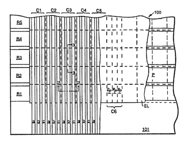
Referring to Figure 1, a portion of an
organic EL device 100 is shown capable of producing a
multicolor image. The upper surface of a light
transmissive, preferably transparent, electrically
insulative planarizing layer 101 is shown bearing a
series of light transmissive, preferably transparent,
first electrodes R1, R2, R3, R4 and R5. The first
electrodes are laterally spaced on the support surface
for electrical isolation in parallel rows. In contact
with and overlying all but the left most extremities of
the first electrodes is an organic EL medium EL.
Overlying the organic EL medium is a series of second
electrodes C1, C2, C3, C4 and C5 arranged in parallel
columns that are laterally spaced one from the other.
The second electrodes extend laterally beyond the lower
2~~~44~
-6-
(as shown in Figure 1) edge of the organic EL medium
onto the lower portion of the planarizing layer. In
each column the electrode is divided into three
parallel laterally spaced elements a, b and c. While
in practice the device can (and in almost every
instance will) have a much larger areal extent than
shown, the portion of the device shown is sufficient to
demonstrate its essential structure.
A grid of intersecting dashed lines are shown
in Figure 1 marking the boundaries of a series of
pixels P. The pixels are arranged in an array of two
intersecting sets of files. One set of files extends
horizontally as shown in Figure 1 and forms rows while
the second set of files extends vertically as shown in
Figure 1 and forms columns. The lower row of pixels in
Figure 1 each overlie the first electrode R1, and each
successive row of pixels overlies one of the successive
first electrodes R2, R3, R4 and R5.
Proceeding from left to right in Figure 1, a
first column of the pixels share the common overlying
second electrode C1 and successive columns of pixels
similarly share successive second electrodes. A column
of pixels C6 is shown in an area where overlying second
electrodes have been broken away for ease of viewing.
In column C6 the pixels are shown to be further divided
into sub-pixels Gp, Rp and Bp. In fact, each column of
pixels is similarly divided, although, for ease of
viewing, this detail is not indicated in each pixel.
The sub-pixels Gp in each column include the overlying
a element of each second electrode, the sub-pixels Rp
in each column include the overlying b element of each
second electrode, and the sub-pixels Bp in each column
include the overlying c element of each second
electrode. The sub-pixels Gp, Rp and Bp differ in that
they emit green, red and blue light, respectively.
208546
The structure of the device that creates the
sub-pixels, the structure that divides the second
electrodes into separate elements, and the manner in
which this structure is fabricated can be appreciated
by reference to Figures 2 and 3. The construction of
the device 100 begins with a light transmissive,
preferably transparent support 105. Polymer and,
particularly, glass supports are generally preferred.
On the upper surface of the support is formed a
patterned fluorescent medium G that emits in the green
and a patterned fluorescent medium R that emits in the
red. Each of the fluorescent media G and R are
patterned to lie in the areas of the Gp and Rp sub-
pixels, respectively. That is, the fluorescent media G
and R are each confined to one sub-pixel column within
each column of pixels P. Fortunately, both the
fluorescent media and support can be selected from
among a variety of materials that are capable of
withstanding conventional patterning techniques, such
as photolithography, without degradation of their
properties.
Together the sub-pixel columns formed by the
green and red fluorescent media account for approxi-
mately two thirds of the area of each column of pixels.
To provide a smooth surface for deposition of the next
layers of the device it is preferred, although not
required, to fill in the columns corresponding to sub-
pixels Hp separating adjacent columns of green and red
fluorescent media. It is possible by conventional
patterning techniques to place a convenient transparent
material in these columns to the exclusion of all other
areas on the support, but the more common approach and
the preferred approach is simply to spin cast the
planarizing layer 101 as shown over all the upper
surfaces of the green and red fluorescent media and the
support, since no patterning is required. This either
._ 2~~~~4~
_8_
entirely eliminates (as shown) or minimizes disparities
in surface height encountered in subsequent coating
steps. Any of a variety of light transmissive,
preferably transparent electrically insulative
conventional planarizing materials can be employed.
Preferred planarizing materials are organic monomers or
polymers that can be polymerized and/or crosslinked
after deposition to create a rigid planar surface. A
rigid planarizing layer can also be produced by sol-gel
glass forming techniques.
Instead of spin casting a planarizing layer
it is alternatively possible simply to place a planar
rigid element that is light transmissive, preferably
transparent and electrically insulative on the surface
of the fluorescent media. Instead of depositing the
fluorescent media on the upper surface of the support
it is also alternatively possible to deposit the
fluorescent media on the lower surface of the rigid
element serving the function of the planarizing layer.
The use of a spin cast planarizing layer rather than an
interposed rigid element is preferred, since this
allows the upper surfaces of the fluorescent media to
be nearer the planar surface being created. When the
planarizing material is confined by patterning to the
areas of sub-pixels HD, the upper surfaces of the
fluorescent media actually form part of the planar
surface being created.
The first electrodes are next formed over the
surface of the planarizing layer. Any convenient
conventional choice of deposition and patterning
techniques can be employed. The planarizing layer
protects the underlying fluorescent media and is itself
capable of withstanding conventional patterning
techniques, such as photolithographic patterning. The
first electrodes are electrically conductive and light
transmissive, preferably transparent. In a
20~~~4(i
_g_
specifically preferred form the first electrodes are
formed of indium tin oxide. A uniform layer of indium
tin oxide can be formed into electrodes by conventional
photolithographic patterning. For example, photoresist
patterning followed by etching of the unprotected
indium tin oxide areas with hydroiodic acid followed in
turn by photoresist removal and rinsing provides the
desired pattern of first electrodes. The planarizing
layer and first electrodes possess a high degree of
chemical stability, allowing photolithography to be
conducted over their surfaces in subsequent fabrication
steps without degradation.
In the preferred form of the invention a
series of parallel walls 107 are next formed over the
first electrodes and the surface of the planarizing
layer adjacent the first electrodes, hereinafter
collectively referred to as the deposition surface.
The walls are located at the shared boundaries of
adjacent sub-pixel columns. The walls can be formed by
any convenient conventional patterning technique.
In a simple, specifically preferred technique
the walls are formed by spin coating a negative working
photoresist onto the deposition surface. A single spin
coating can conveniently produce a photoresist layer
thickness of up to 20 ~tm, well in excess of the minimum
wall height required for the devices of this invention.
Patterned exposure crosslinks the photoresist to an
insoluble form in exposed areas while unexposed areas
can be removed by development and washing techniques.
Crosslinking by exposure produces strong, relatively
rigid walls.
Numerous alternative wall forming techniques
are possible. Instead of spin casting and using a
photoresist developer, two 'wet chemistry' steps, a
photoresist layer can be formed on the support by
laminating a photoresist coating on a flexible support,
2a~544fi
-10-
such as transparent film, to the supporting surface.
In this form the photoresist is typically a monomer
that is polymerized by imagewise exposure following
lamination. After imagewise exposure stripping the
film also removes the monomer in areas that are not
exposed. No "wet chemistry" step is entailed.
In another wall forming technique the
photoresist does not form the walls, but defines the
wall pattern by its presence in areas surrounding the
walls on the supporting surface. Fhotoresist layer
formation can take any of the forms described above,
but imagewise exposure is chosen to leave the
photoresist in the areas surrounding the walls. Either
a positive or negative working photoresist can be
employed. Subsequently a wall forming material, such
as silica, silicon nitride, alumina, etc., is deposited
uniformly so that it overlies the photoresist where
present and is deposited on the deposition surface in
wall areas. After the walls are formed, the
photoresist can be removed by any convenient
conventional technique--e. g. solvent lift-off.
After the walls are formed along common
boundaries of adjacent sub-pixel columns, the organic
EL medium EL is next deposited by any convenient
conventional vapor phase deposition technique over the
walls and the remainder of the deposition surface. As
shown in Figure 1 the left and lower edges of the
deposition surface are free of the organic EL medium so
that the portions of the electrode elements extending
into these areas are available for external electrical
lead attachments. These laterally extended portions of
the electrode elements are commonly referred to as
bonding pads. A mask, such as a strip of tape, along
the edges of the substrate adjacent bonding pad sites
can be used to define the deposition pattern of the
organic EL medium. Alternatively, the organic EL
-11-
medium can be deposited over the entire deposition
surface and then mechanically removed by abrasion.
Generally any vapor phase deposition
technique can be employed known to be useful in
depositing one or more layers of an organic EL medium.
It is generally preferred that the height of the walls
be chosen to exceed the thickness of the organic EL
medium. In efficient device constructions the organic
EL medium, even when present in multilayer forms, has a
thickness of less than 1 ~tm (10,000 ~) and typically
less than half this thickness. Hence achieving useful
wall heights is well within the capabilities of
conventional patterning techniques useful for wall
formation.
Following deposition of the organic EL
medium, a source is provided for the metals used for
deposition of the secand electrode elements. For
efficient organic EL devices the second electrode
elements require a metal having a lower (less than 4.0
eV) work function to be in contact with the organic EL
medium. One or more low work function metals alone or
combination with one or more higher work function
metals are deposited on the organic EL medium by any
convenient directional (i.e.. line of sight) transport
technique. To insure linear transport from their
source to the organic EL medium surface the metal atoms
are preferably transported through a reduced pressure
atmosphere. This increases the mean free path of the
metal ions during transport from the source to the
surface of organic EL medium, thereby minimizing
scattering and maintaining deposition in a
directionally controlled manner. Generally the
pressure of the ambient atmosphere during deposition is
reduced so that the spacing between the source and the
surface of the organic EL medium is less than the mean
free travel path of the metal atoms (that is, less than
~08~448
-12-
the distance a metal atom on average travels before
colliding an atom in the ambient atmosphere).
Conventional deposition techniques compatible with the
directional transport requirements include vacuum vapor
deposition, electron beam deposition, ion beam
deposition, laser ablation and sputtering.
To achieve a deposition pattern of the second
electrode elements in laterally spaced columns the
deposition surface is positioned in relation to the
source of metal to be deposited so that each wall is
interposed between the source and an adjacent portion
of the surface of the organic EL medium. When
deposition is undertaken in such an orientation the
interposed portions of the walls intercept metal atoms
travelling from the source, thereby preventing metal
deposition on the organic EL medium on one side of each
wall. This provides the spacing between adjacent rows
of second electrode elements. Convenient preferred
ranges of orientations in relation to the source of
metal atoms are established when the direction of
travel of the metal atoms (or the line of sight between
the source) and the deposition surface indicated by
arrow A forms an angle 61 with the normal of the
deposition surface (an axis normal to the deposition
surface) of from about 10° to 60°, most preferably from
about 15° to 45°.
Deposition of low (<4.0 eV) work function
metal, alone or in combination of one or more higher
work function metals, requires only that a continuous
layer containing the low work function metal be
deposited to achieve maximum efficiency of electron
injection into the organic EL medium. However, to
increase conductance (decrease resistance), it is
preferred to increase the thickness of the second
electrode elements beyond the 200 to 500 ~ thickness
levels contemplated to provide a continuous layer.
2~8~44~
-13-
Although thick electrodes of up to 1 ~tm or even higher
can be formed using the original metal composition, it
is generally preferred to switch deposition after
initial formation of continuous layers containing low
~5 work function metal so that only relatively higher work
function (and hence less chemically reactive) metals
are deposited. Fox example, an initial continuous
layer of magnesium (a preferred low work function
metal) and silver, indium or aluminum would preferably
be increased in thickness for the purpose of reducing
second electrode element resistance by depositing a
convenient higher work function metal commonly used in
circuit fabrication, such as gold, silver, copper
and/or aluminum. The combination of a lower work
function metal at the interface of the organic EL
medium and a higher work function metal completing the
thickness of the overlying second electrode elements is
particularly advantageous, since the higher electron
injection efficiencies produced by a lower work
function metal are fully realized even though the lower
work function metal is limited to the second electrode
element interface with the organic EL medium while the
presence of the higher work metal increases the
stability of the second electrode elements. Hence, a
combination of high injection efficiency and high
electrode element stability is realized by this
arrangement.
In operation a selected pattern of light
emission from the device 100 is produced that can be
seen by viewing the bottom surface of the transparent
support 105. In a preferred mode of operation the
device is stimulated to emit by sequentially
stimulating one row of pixels at a time and repeating
the stimulating sequence at a rate chosen so that the
interval between repeated stimulations of each row is
less than the detection limit of the human eye,
2
-14-
typically less than about 1/60th of a second. The
viewer sees an image formed by emission from all
stimulated rows, even though the device at.any instant
is emitting light from only one row.
To create the desired image pattern, the a, b
and c elements of each of the second electrodes are
independently electrically addressed while the first
electrode R1 is electrically biased to support
emission. If, for example, only green emission is
wanted and that in only the columns including second
electrodes C2, C3 and C4, the a elements in these
columns are biased to support emission while the
remaining second electrode elements are not
electrically biased or given a bias of a polarity
opposite that required to support emission.
Immediately following emission in the desired pattern
from the row of pixels joined by first electrode R1, a
new pattern of stimulation is supplied to the second
electrode elements, and the first electrode element R2
is next biased to stimulate the desired pattern of
emission from the row of pixels it joins. Stimulation
of patterned emission from successive rows is achieved
by repeating the procedure described above while
biasing successive first electrodes.
The organic EL medium EL is selected so that
it emits in the blue region of the spectrum. In the
blue emitting sub-pixels Hp light emitted by the
organic EL medium penetrates the first electrodes, the
planarizing layer (when present) and the support and is
seen by the viewer as blue light.
In the green and red emitting pixels the same
blue emitting organic EL medium is employed as in the
blue emitting sub-pixels. The blue light emitted again
penetrates the first electrodes and the planarizing
layer (when present), but in the sub-pixels GD and Rp
the fluorescent media Q and R, respectively, intercept
2U~~446
-15-
and absorb the blue light emitted by the organic EL
medium. The blue light stimulates fluorescent emission
in the green or red.
A very significant advantage of absorbing
blue light emission from the organic EL medium and
reemitting longer wavelength, green or red, light by
fluorescence is that the efficiency of light emission
can be very much superior to that achieved employing a
color filter array in combination with a white light
emitting organic EL medium. In the latter arrangement
a theoretical maximum efficiency of only 33 percent is
possible, since each sub-pixel of the color filter
array absorbs and does not transmit two-thirds of the
photons it receives. Further, aside from efficiency
losses due to the color filter array, it is to be noted
that the organic EL medium cannot be optimized to emit
in any one portion of the visible spectrum, but must
emit throughout the visible spectrum. This places a
further efficiency burden on this conventional
arrangement and results in its overall efficiency as a
practical matter being substantially less than 33
percent.
The efficiency of the present invention is
controlled by (a) the efficiency of emission of blue
light by the organic EL medium, (b) the efficiency with
which the blue light is absorbed by the fluorescent
media, and (c) the efficiency with which fluorescent
media is stimulated to emit longer wavelength light.
Considering (a) first, it is apparent that the blue
emitting organic EL medium employed in the device 100
can be selected from a variety of highly efficient
materials that would be highly inefficient in providing
emission in each of the blue, green and red portions of
the spectrum (i.e., in providing white light emission).
Turning to (b), high levels of efficiency can be
realized in absorbing blue light emitted by the organic
20~~~4~
-16-
EL medium. There is no reason in theory why 100% of
the blue light emitted can not be absorbed by the
fluorescent medium. It is contemplated that in all
instances at least 50% and preferably at least 80% of
blue light emitted in the green and red sub-pixels can
be absorbed. Turning to (c), a variety of fluorescent
materials are known that are capable of emitting at
least 50% of the light they absorb and emission
efficiencies in excess of 80% of light absorption are
contemplated. Thus, within readily attainable levels
of blue light absorption and longer wavelength
fluorescence efficiencies, the green and red sub-pixels
are capable of delivering to the viewer substantially
greater than half the number of photons received from
the blue emitting organic EL medium. For example,
assuming an absorption efficiency of 80% and a
fluorescence efficiency of 80%, both of which are
readily attainable, 64% of the photons received from
the organic EL medium are transmitted to the viewer in
areas containing the fluorescent medium. In the blue
sub-pixel areas, the efficiency is approximately 100%,
since light absorption in the transparent electrode,
planarizing layer (when present) and support can be
negligible or nearly negligible.
Another significant advantage of the device
100 is that no patterning of the organic EL medium in
pixel areas is required. This avoids the significant
degradations in performance of conventional organic EL
devices after patterning. For example, the
construction of the device 100 requires no wet
chemistry for patterning during or after deposition of
the organic EL medium. No photolithographic patterning
steps are required and no wet etching steps are
required to be performed after the organic EL medium is
deposited. This protects both the organic EL medium
2~&~~4~
-17-
and the overlying second electrode elements from
degradation.
The device 100 has the capability of full
color imaging. Employing blue, green and red primary
color emissions, the following emission combinations
are possible from each pixel:
(a) stimulate one sub-pixel to emit blue;
(b) stimulate one sub-pixel to emit green;
(c) stimulate one sub-pixel to emit red;
(d) stimulate two sub-pixels to emit blue and
green, creating the perception of cyan;
(e) stimulate two sub-pixels to emit blue and
red, creating the perception of magenta;
(f) stimulate two sub-pixels to emit green and
red, creating the perception of yellow;
(g) stimulate all sub-pixels to create white
light emission; and
(h) stimulate none of the sub-pixels to provide a
dark, essentially black background.
Although the multicolor image display device
100 fully satisfies the requirements of the invention,
the device exhibits some disadvantages. First,
referring to Figure 1, it is apparent that in
successively biasing each first electrode it must carry
current to each of the pixels in the same row that is
to emit light. Hence, the current carried by each
first electrode is the sum of the currents carried by
each of the second electrode elements in stimulating a
row of pixels to emit light. The disadvantage of this
arrangement is that the first electrodes must be light
transmissive for light emissions to be seen and their
thicknesses must be limited to retain this property.
However, limiting first electrode thickness also limits
conductance.
If the pixels are addressed in columns rather
than rows, each of the second electrode elements a, b
2~~~~4~
and c must carry the current of all pixels in the same
column. Although the thickness of the second electrode
elements can and usually does exceed that of the first
electrodes, the width of the second electrode elements
must be less than the width of a sub-pixel. As a
consequence, the conductance of the second electrode
elements is also restricted. Further, addressing the
pixels column by column is unattractive, since in an
array having an equal number of pixels in columns and
rows the addressing rate for columns must be three
times that employed for rows, since each column
contains three second electrode elements. Since the
time in which the sub-pixels in a column can be biased
to emit light is reduced to one third that required for
row by row addressing, the biasing voltage must be
increased as compared to row addressing to maintain a
sub-pixel coulomb level and emission level during
biasing equal to that obtained with row by row
addressing. Increased biasing voltages and tripled
addressing rates for comparable emission properties
represent a significant disadvantage.
The multicolor organic EL image display
device 200 shown in Figure 4 exhibits all of the
imaging capabilities of the device 100 while at the
same time overcoming its disadvantages noted above.
Except as specifically noted, the features of the
device 200 can take any of the forms described in
connection with the device 100 and therefore require no
further explanation.
The first electrodes C10, C11, C12, C13, C14,
C15, C16 and C17 of device 200 are each divided into
elements c, 8 and e. These first electrode elements
have the light transmissive properties of the first
electrodes of device 100 and, like the first electrodes
of device 100, are formed prior to depositing the
organic EL medium. Each first electrode element c
z~s~~~~~
-19-
forms a part of and joins sub-pixels Gp in the same
column; each first electrode element d forms a part of
and joins sub-pixels Rp in the same column; and each
third electrode element a forms a part of and joins
sub-pixels Bp in the same column. The second
electrodes R10, R11 and R12 can be constructed of the
same materials and in the same thickness ranges as the
second electrode elements of device 100, but are
arranged in rows rather than columns. The row
arrangement allows the second electrodes to be wider
than the second electrodes of device 100.
The electrode arrangement of the device 200
achieves higher electrode conductances than can be
realized in device 100. In addressing a row of pixels
each of the first electrode elements c, d and a is
biased independently to achieve the desired pattern of
emission from the pixels in one row. Simultaneously
one of the second electrodes is biased to stimulate
emission within a selected row. Each of the first
electrode elements stimulates only one sub-pixel and
carries only the current of one sub-pixel. The second
electrode in the selected row carries the current of
all the sub-pixels stimulated to emit in that row.
Since the second electrodes need not be light
transmissive and, hence, can be much thicker as well as
wider than the first electrode elements, the
conductance of the electrodes of device 200 can be
higher than that of the electrodes of device 100.
The construction of one of the pixels P of
the device 200 is shown in Figures 5 and 6. The
support 205, the patterned fluorescent media G and R,
and the planarizing layer 201 are identical to
corresponding elements in device 100. Except far the
differences in patterning noted above, the first
electrode elements c, d and e, the organic EL medium EL
i ~~ i
CA 02085446 2002-08-27
-20-
and the second electrodes are constructed similarly as
described in connection with device 100.
In comparing Figures 2 and 6 it is apparent
that the device 200 offers a significant structural
advantage in the construction of the walls Z07. These
walls are located at the shared boundaries of adjacent
rows of pixels. The device 200 contains fewer walls
than device 100. Whereas in device 100 the number of
walls is three times the number of pixel columns (plus
one additional wall), in device a00 the number of walls
is equal to the number of rows (plus one additional
wall). For arrays containing an equal number of pixels
in rows and columns there is approximately a 3 to 1
reduction in the number of walls that need be formed.
The materials of the image display organic EL
devices of this invention can take any of the forms of
conventional organic EL devices, such as those of
Scozzafava, cited above; Tang U.S. Patent 4,356,429;
VanSlyke et al U.S. Patent 4,539,507; VanSlyke et al
U.S. Patent 4,720,432; Tang et al U.S. Patent
4,885,211; Tang et al U.S. Patent 4,769,292; Perry et
al U.S. Patent 4,950,950; Littman et al U.S. Patent No.
5,059,861; VanSlyke U.S. Patent 5,047,687;
Canadian Patent 2,046,220; VanSlyke et al U.S. Patent
5,059,862; VanSlyke et al U.S. Patent 5,061,617.
A specifically preferred support for the
devices of the invention is a transparent glass
support. The preferred first electrodes of the devices
of this invention are transparent indium tin oxide
electrodes coated directly on the glass support.
Instead of employing indium tin oxide, tin oxide or a
similar electrically conductive transparent oxide, the
first electrode elements can be formed of thin, light
transmissive layers of any of the high (e. g., greater
than 4.0 eV) work function metals. Chromium and gold
-21-
mixtures are particularly contemplated for forming the
first electrodes. The first electrodes are typically
in the range of from 1 Eun (10,000 ~) to 500 ~ in
thickness, preferably in the range of from 3000 ~ to
1000 ~ in thickness.
As illustrated in Figure 7, the organic EL
medium EL coated over the first electrodes, represented
by a first electrode E1, is preferably made up of a
sequence of four superimposed layers. The layer in
direct contact with each first electrode is a hole
injecting layer HI that receives holes from the first
electrode E1 when it is positively biased relative to a
second electrode E2. In contact with and overlying the
hole injecting layer is a hole transporting layer HT.
The hole injecting layer and the hole transporting
layer together form a hole injecting and transporting
zone HIT. Overlying and in contact with the hole
injecting and transporting zone is an electron
injecting and transporting zone EIT formed by an
electron injecting layer EI in contact with the second
electrode and a luminescent layer LU. 4rhen the second
electrode E2 is negatively biased in relation to the
first electrode E1, electrons are received from the
second electrode by the layer EI which in turn injects
electrons into the luminescent layer LU. Concurrently
holes are injected from the hole transporting layer HT
into the luminescent layer. Hole-electron recombin-
ation in layer LU results in electroluminescence.
A functioning device requires only the
luminescent layer LU between and in contact with the
first and second electrodes. A marked increase in
efficiency is realized when a two layer organic EL
medium construction is employed consisting of the
luminescent layer LU and the hole injecting layer HI.
Each of the layers Ei and HT independently contribute
to achieving the highest levels of stability and
~~~r- 3
-22-
efficiency. The the organic EL medium can be
constructed of from one to four of the layers
described, with only the luminescent layer LU being
essential to operability.
The hole injecting layer is preferably
comprised of a porphyrinic compound of the type
disclosed by Adler U.S. Patent 3,935,031 or Tang
U.S. Patent 4,356,429.
Preferred porphyrinic compounds are those
of structural formula (I):
(I)
T2 Tt
t ~ ~ t
T N ~ T
I ~N-M-N ~ I
T2 Q N ~~ T2
i
T' T2
wherein
Q is -N= or -C(R)=;
M is a metal, metal oxide, or metal halide;
R is hydrogen, alkyl, aralkyl, aryl, or alkaryl,
and
T1 and T2 represent hydrogen or together
complete a unsaturated 6 membered ring, which can
include substituents, such as alkyl or halogen.
Preferred alkyl moieties contain from about 1 to 6
carbon atoms while phenyl constitutes a preferred
aryl moiety.
In an alternative preferred form the
porphyrinic compounds differ from those of structural
-23-
formula (I) by substitution of two hydrogens for the
metal atom, as indicated by formula (II):
(II)
TZ T'
T' Q N ~ T~
I_~ N H N ~ I
T2 Q N \T2
,Q
T' TZ
Highly preferred examples of useful
porphyrinic compounds are metal free phthalocyanines
and metal containing phthalocyanines. 4~lhile the
porphyrinic compounds in general and the phthalo-
cyanines in particular can contain any metal, the
metal preferably has a positive valence of two or
higher. Exemplary preferred metals are cobalt,
magnesium, zinc, palladium, nickel, and,
particularly, copper, lead, and platinum.
Illustrative of useful porphyrinic
compounds are the following:
PC-1 Porphine
PC-2 1,10,15,20-Tetraphenyl-21H,23H-porphine
copper (II)
PC-3 1,10,15,20-Tetraphenyl-21H,23H--porphine
zinc (II)
PC-4 5,10,15,20-Tetrakis(pentafluorophenyl)-
21H,23H-porphine
PC-5 Silicon phthalocyanine oxide
PC-6 Aluminum phthalocyanine chloride
PC-7 Phthalocyanine (metal free)
2U8~~4~
-24-
PC-8 Dilithium phthalocyanine
PC-9 Copper tetramethylphthalocyanine
PC-10 Copper phthalocyanine
PC-11 Chromium phthalocyanine fluoride
PC-12 Zinc phthalocyanine
PC-13 Lead phthalocyanine
PC-14 Titanium phthalocyanine oxide
PC-15 Magnesium phthalocyanine
PC-16 Copper octamethylphthalocyanine
The hole transporting layer preferably
contains at least one hole transporting aromatic
tertiary amine, where the latter is understood to be
a compound containing at least one trivalent nitrogen
atom that is bonded only to carbon atoms, at least
one of which is a member of an aromatic ring. In one
form the aromatic tertiary amine can be an arylamine,
such as a monoarylamine, diarylamine, triarylamine,
or a polymeric arylamine. Exemplary monomeric
triarylamines are illustrated by Klupfel et al U.S.
Patent 3,180,730. Other suitable triarylamines
substituted with vinyl or vinylene radicals and/or
containing at least one active hydrogen containing
group are disclosed by Brantley et al U.S. Patents
3,567,450 and 3,658,520.
A preferred class of aromatic tertiary
amines are those which include at least two aromatic
tertiary amine moieties. Such compounds include
those represented by structural formula (III):
(III)
Q1 Q2
\ /
G
wherein
Q1 and Q2 are independently aromatic tertiary
amine moieties and
-25-
G is a linking group such an arylene, cyclo-
alkylene, or alkylene group or a carbon to carbon
bond.
A particularly preferred class of
triarylamines satisfying structural formula (III) and
containing two triarylamine moieties are those
satisfying structural formula (IV):
(IV)
R2
I
R1_ C _ R3
I
R~
where
R1 and R2 each independently represents a
hydrogen atom, an aryl group or alkyl group or R1 and
R2 together represent the atoms completing a
cycloalkyl group and
R3 and R4 each independently represents an aryl
group which is in turn substituted with a diaryl
substituted amino group, as indicated by structural
formula (V):
(V)
R5
- N
R6
wherein R5 and R6 are independently selected aryl
groups.
Another preferred class of aromatic
tertiary amines are tetraaryldiamines. Preferred
tetraaryldiamines include two diarylamino groups,
such as indicated by formula (IV), linked through an
arylene group. Preferred tetraaryldiamines include
those represented by formula (VI).
2~~~44~
-26-
(VI)
R7 R8
\ /
N Aren N
/ \
Ar R9
wherein
Are is an arylene group,
n is an integer of from 1 to 4, and
Ar, R7, R8, and R9 are independently
selected aryl groups.
The various alkyl, alkylene, aryl, and
arylene moieties of the foregoing structural formulae
(III), (IV), (V), and (VI) can each in turn be
substituted. Typical substituents including alkyl
groups, alkoxy groups, aryl groups, aryloxy groups,
and halogen such as fluoride, chloride, and bromide.
The various alkyl and alkylene moieties typically
contain from about 1 to 5 carbon atoms. The
cycloalkyl moieties can contain from 3 to about 10
carbon atoms, but typically contain five, six, or
seven ring carbon atoms--e. g., cyclopentyl,
cyclohexyl, and cycloheptyl ring structures. The
aryl and arylene moieties are preferably phenyl and
phenylene moieties.
Representative useful aromatic tertiary
amines are disclosed by Berwick et al U.S. Patent
4,175,960 and Van Slyke et al U.S. Patent 4,539.507.
Berwick et al in addition discloses as useful hole
transporting compounds N substituted carbazoles,
which can be viewed as ring bridged variants of the
diaryl and triarylamines disclosed above.
Following the teachings of VanSlyke et al
U.S. Patent 5,061,569, cited above, it is possible to
achieve higher organic EL device stabilities both
during short term and extended operation by
2~1~a~4~
-27-
substituting for one or more of the aryl groups
attached directly to a tertiary nitrogen atom in the
aromatic tertiary amines described above an aromatic
moiety containing at least two fused aromatic rings.
The best combination of both short term (0-50 hours)
and long term (0-300+ hours) of operation are
achieved when the aromatic tertiary amines are those
which (1) are comprised of at least two tertiary
amine moieties and (2) include attached to a tertiary
amine nitrogen atom an aromatic moiety containing at
least two fused aromatic rings. The fused aromatic
ring moieties of the tertiary amines can contain 24
or more carbon atoms and preferably contain from
about 10 to 16 ring carbon atoms. While unsaturated
5 and 7 membered rings can be fused to six membered
aromatic rings (i.e., benzene rings) to form useful
fused aromatic ring moieties, it is generally
preferred that the fused aromatic ring moiety include
at least two fused benzene rings. The simplest form
of a fused aromatic ring moiety containing two fused
benzene rings is naphthalene. Therefore, the
preferred aromatic ring moieties are naphthalene
moieties, where the latter is understood to embrace
all compounds containing a naphthalene ring
structure. In manovalent form the naphthalene
moieties are naphthyl moieties, and in their divalent
form the naphthalene moieties are naphthylene
moieties.
Illustrative of useful aromatic tertiary
amines are the following:
ATA-1 1,1-Bis(4-di-p-tolylaminophenyl)cyclohexane
ATA-2 1,1-Bis(4-di-p-tolylaminophenyl)-4-phenyl-
cyclohexane
ATA-3 4,4 " '-Bis(diphenylamino)quaterphenyl
ATA-4 Bis(4-dimethylamino-2-methylphenyl)phenylmethane
20~54~46
-28-
ATA-5 N,N,N-Trip-tolyl)amine
ATA-6 4-(di-p-tolylamino)-4'-[4(di-p-tolylamino)-
styryl]stilbene
ATA-7 N,N,N',N'-Tetra-p-tolyl-4,4'-diaminobiphenyl
ATA-8 N,N,N',N'-Tetraphenyl-4,4'-diaminobiphenyl
ATA-9 N-Phenylcarbazole
ATA-10 Poly(N-vinylcarbazole)
ATA-11 4,4'-Bis[N-(1-naphthyl)-N-phenylamino]biphenyl
ATA-12 4,4"-Bis[N-(1-naphthyl)-N-phenylamino]-p-ter-
phenyl
ATA-13 4,4'-Bis[N-(2-naphthyl)-N-phenylamino]biphenyl
ATA-14 4,4'-Bis[N-(3-acenaphthenyl)-N-phenylamino]bi
phenyl
ATA-15 1,5-Bis[N-(1-naphthyl)-N-phenylamino]naphthalene
ATA-16 4,4'-Bis[N-(9-anthryl)-N-phenylamino]biphenyl
ATA-17 4,4"-Bis[N-(1-anthryl)-N-phenylamino]-p-ter-
phenyl
ATA-18 4,4'-Bis[N-(2-phenanthryl)-N-phenylamino]bi-
phenyl
ATA-19 4,4'-Bis[N-(8-fluoranthenyl)-N-phenylamino]bi-
phenyl
ATA-20 4,4'-Bis[N-(2-pyrenyl)-N-phenylamino]biphenyl
ATA-21 4,4'-Bis[N-(2-naphthacenyl)-N-phenylamino]bi
phenyl
ATA-22 4,4'-Bis[N-(2-perylenyl)-N-phenylamino]biphenyl
ATA-23 4,4'-Bis[N-(1-coronenyl)-N-phenylamino]biphenyl
ATA-24 2,6-Bis(di-~-tolylamino)naphthalene
ATA-25 2,6-Bis[di-(1-naphthyl)amino]naphthalene
ATA-26 2,6-Bis[N-(1-naphthyl)-N-(2-naphthyl)amino]naph-
thalene
ATA-27 4,4"-Bis[N,N-di(2-naphthyl)amino]terphenyl
ATA-28 4,4'-Bis{N-phenyl-N-[4-(1-naphthyl)phenyl]-
amino}biphenyl
ATA-29 4,4'-Bis[N-phenyl-N-(2-pyrenyl)amino]biphenyl
ATA-30 2,6-Bis[N,N-di(2-naphthyl)amine]fluorene
ATA-31 4,4"-Bis(N,N-di-p-tolylamino)terphenyl
i i1 i
CA 02085446 2002-08-27
-29-
ATA-32 Bis(N-1-naphthyl)(N-2-naphthyl)amine
Any conventional blue emitting organic
electroluminescent layer can be employed to form the
layer LU. The term blue emitting" is herein employed
to indicate that visible emission occurs principally in
the blue portion of the spectrum--that is, in the
spectral region of from 400 to 500 nm. However, if the
wavelength of peak emission is too near the green, a
significant green emission can accompany the blue
emission. It is therefore preferred to select blue
emitting materials that exhibit a peak emission
wavelength of less than 480 nm. Note that a peak
emission in the near ultraviolet is not detrimental to
the obtaining a blue hue of emission. Thus, so long as
the electroluminescent layer is blue emitting it is
immaterial whether peak emission occurs at wavelengths
longer than or shorter than 400 nm.
It is preferred to employ mixed ligand
aluminum chelates of the type disclosed by
U.S. Patent 5,150,006.
In a specifically preferred form the mixed
ligand aluminum chelates therein disclosed include
bis(Rs-8-quinolinolato)-(phenolato)aluminum(III)
chelate, where Rs is a ring substituent of the 8-
quinolinolato ring nucleus chosen to block the
attachment of more than two 8-quinolino-lato ligands to
the aluminum atom. These compounds can be represented
by the formula:
(VII)
(Rs_Q) 2-p,l-0-L
where
-30-
Q in each occurrence represents a substituted
8-quinolinolato ligand,
RS represents an 8-quinolinolato ring substituent
chosen to block sterically the attachment of more than
two substituted 8-quinolinolato ligands to the aluminum
atom,
O-L is phenolato ligand, and
L is a hydrocarbon of from 6 to 24 carbon atoms
comprised of a phenyl moiety.
The advantage of employing an aluminum
chelate with two substituted 8-quinolinolato ligands
and a phenolato ligand is that all of the desirable
physical properties of tris(8-quinolinolato)alumin-
um(III) chelates, the preferred green emitting
luminophors of organic EL devices, are retained while
emission is shifted to the blue region of the spectrum.
The presence of the phenolato ligand is
responsible for shifting emissions to the blue portion
of the spectrum. As employed herein the term
"phenolato ligand" is employed in its art recognized
usage to mean a ligand bonded to the aluminum atom by
the deprotonated hydroxyl group of a phenol.
In its simplest form the phenolato ligand can
be provided by deprononation of hydroxybenzene.
Organic EL device performance has demonstrated that
peak emission at a shorter wavelength than 500 nm and
acceptable device stability (retention of at least a
half of initial luminescent intensity for more than 50
hours) can be realized.
In an effort to improve performance,
substituted phenols were next investigated. It was
observed that methoxy and dimethoxy substituted
phenolato ligands exhibited relatively weak luminescent
intensities. Since methoxy substituents are electron
donating, phenols were also investigated with strongly
electron withdrawing substituents, such as halo, cyano
2~~~~~6
-31-
and a-haloalkyl substituents. Aluminum chelates with
these ligands, though luminophors, did not undergo
successful vapor phase conversions.
It has been determined that the preferred
phenolato ligands for the aluminum chelates of formula
VII are derived from HO-L phenols, where L is a
hydrocarbon of from 6 to 24 carbon atoms comprised of a
phenyl moiety. This includes not only hydroxybenzene,
but a variety of hydrocarbon substituted
hydroxybenzenes, hydroxynaphthalenes and other fused
ring hydrocarbons. Since monomethyl substitution of
the phenyl moiety shorten emission wavelengths, it is
preferred that the phenolato ligand contain at least 7
carbon atoms. Generally there is little advantage to
be gained by employing phenolato ligands with very
large numbers of carbon atoms. However, investigations
of phenolato ligands with 18 aromatic ring carbon atoms
have revealed high levels of stability. Thus, the
phenolato ligands preferably contain from 7 to 18 total
carbon atoms.
Aliphatic substituents of the phenyl moiety
of phenolato ligand are contemplated to contain from 1
to 12 carbon atoms each. Alkyl phenyl moiety
substituents of from 1 to 3 carbon atoms are
specifically preferred, with the best overall
characteristics having been observed to be produced
with methyl substituents.
Aromatic hydrocarbon substituents of the
phenyl moiety are preferably phenyl or naphthyl rings.
Phenyl, diphenyl and triphenyl substitution of the
phenyl moiety have all been observed to produce highly
desirable organic EL device characteristics.
Phenolato ligands derived from a or
naphthols have been observed to produce aluminum
chelates of exceptional levels of stability. A limited
degree of emission shifting to shorter wavelengths is
208~44~
-32-
also realized, similar to that exhibited by
hydroxybenzene derived phenolato ligands. By employing
naphtholato ligand containing aluminum chelates in
combination with blue emitting fluorescent dyes,
described below, highly desirable device constructions
are possible.
From comparisons of ortho, meta and para
substituted homologues of the various phenolato ligands
it has been determined that little, if any, difference
in performance is attributable to the position on the
phenyl moiety ring occupied by the hydrocarbon
substituent.
In a preferred form the aluminum chelates
satisfy the following formula:
(VIII)
L' L~
(RS-Q)Z-A i-0
L5 \L4
where
Q and RS are as defined above and
L1, L2, L3, L4 and L5 collectively contain 12 or
fewer carbon atoms and each independently represent
hydrogen or hydrocarbon groups of from 1 to 12 carbon
atoms, with the proviso that L1 and L2 together or L2
and L3 together can form a fused benzo ring.
Although either or both of the 8-quino-
linolato rings can contain substituents other than the
steric blocking substituent, further substitution of
the rings is not required. It is appreciated further
that more than one substituent per ring can contribute
285446
-33-
to steric blocking. The various steric blocking
substituent possibilities are most easily visualized by
reference to the following formula:
(IX)
R6 R'
Rs / \
- ~A i-p- L
R4 \ ~N
R \R2
2
where L can take any form described above and R2 to R~
represent substitutional possibilities at each of ring
positions 2 to 7 inclusive of the 8-quinolinolato
rings. Substituents at the 4, 5 and 6 ring positions
are not favorably located to hinder sterically the
bonding of three 8-quinolinolato nuclei to a single
aluminum atom. While it is contemplated that large
substituents at the 3 or 7 ring positions could provide
sufficient steric hindrance, the incorporation of bulky
substituents substantially increases molecular weight
without enhancing molecular performance and therefore
detracts from overall performance. On the other hand,
the 2 ring position is suited to provide steric
hindrance, and even a very small substituent (e.g., a
methyl group) in one of these ring positions provides
an effective steric blocking substituent. For
synthetic convenience it is specifically preferred that
steric blocking substituents be located in the 2 ring
positions. As employed herein the term 'steric
blocking is employed to indicate that the Rs-Q ligand
..~ 2os~~~~
-34-
is incapable of competing for inclusion as the third
ligand of the aluminum atom.
Although the phenolato ligand is primarily
relied upon to obtain blue emission, it has been
observed that substituents to the 8-quinolinolato rings
can also perform useful hue shifting functions. The
quinoline ring consists of fused benzo and pyrido
rings. When the pyrido ring component of the quinoline
ring is substituted with one or more electron donating
substituents the effect is to shift the hue of emission
away from the green region of the spectrum and toward a
more primary blue emission. Electron donating
substituents at the ortho and para positions of the
pyrido ring (that is, the 2 and 4 positions of the
quinoline ring) particularly influence the hue of
emission, while the meta position on the pyrido ring
(the 3 position on the quinoline ring) has a
comparatively small influence on the hue of emission.
It is, in fact, recognized that an electron accepting
substituent could, if desired, be located at the 3 ring
position while retaining a blue emission
characteristic. Although steric hindrance is entirely
independent of electron donating or accepting
properties and, thus, R2 can in theory take the form of
either an electron donating or accepting group, it is
preferred to choose R2 from among electron donating
groups. By adding a second electron donating group R4
a further shift in hue away from the green portion of
the spectrum is achieved. R3, when present, can take
any synthetically convenient form, but is preferably
also electron donating.
It is well within the skill of the art to
determine whether a particular substituent is electron
donating or electron accepting. The electron donating
or accepting properties of several hundred of the most
common substituents, reflecting all common classes of
~0~~~4fi
-3 5-
substituents have been determined, quantified and
published. The most common quantification of electron
donating and accepting properties is in terms of
Hammett a values. Substituents with negative Hammett a
values are electron donating while those with positive
Hammett a values are electron accepting. Hydrogen has
a Hammett a value of zero, while other substituents
have Hammett a values that increase positively or
negatively in direct relation to their electron
accepting or donating characteristics. Lange's
Handbook of Chemistry, 12th Ed., McGraw Hill, 1979,
Table 3-12, pp. 3-134 to 3-138, lists Hammett 6 values
for a large number of commonly encountered
substituents. Hammett a values are assigned based on
phenyl ring substitution, but they provide a workable
guide for qualitatively selecting electron donating and
accepting substituents for the quinoline ring.
Taking all factors together, steric blocking,
synthetic convenience, and electron donating or
accepting properties, R2 is preferably an amino, oxy or
hydrocarbon substituent. Adequate steric hindrance is
provided when R2 is methyl and is the sole 8-quinolino-
lato ring substituent (i.e., each of R3, R4, R5, R6 and
R7 is hydrogen). Thus, any amino, oxy or hydrocarbon
substituent having at least 1 carbon atom falls within
the preview of preferred substituents. Preferably no
more than 10 carbon atoms are present in any one
hydrocarbon moiety and optimally no more than 6 carbon
atoms. Thus, R2 preferably takes the form of -R', -OR'
or -N(R')R', where R' is a hydrocarbon of from 1 to 10
carbon atoms and R' is R' or hydrogen. Preferably R2
contains 10 or fewer carbon atoms and optimally 6 or
fewer carbon atoms.
R3 and R4 for the reasons set forth above can
take a broader range of forms than R2, but are
specifically contemplated to be selected from among the
248~44~
-36-
same group of preferred substituents as R2. Since 3
and 4 ring position substitution is not required, R3
and R4 can additionally be hydrogen.
Since 5, 6 or 7 ring position substitution is
not required, R5, R6 and R~ can represent hydrogen. In
preferred forms R5, R6 and R~ can be selected from
synthetically convenient electron accepting
substituents, such as cyano, halogen, and a-haloalkyl,
a-haloalkoxy, amido, sulfonyl, carbonyl, carbonyloxy
and oxycarbonyl substituents containing up to 10 carbon
atoms, most preferably 6 or fewer carbon atoms.
The following constitute specific examples of
preferred mixed ligand aluminum chelates satisfying the
requirements of the invention:
PC-1 Bis(2-methyl-8-quinolinolato)(phenolato)-
aluminum(III)
~ 0
A I-~ \ /
,N
CHy
2
PC-2 Bis(2-methyl-8-quinolinolato)(ortho-cres-
olato)aluminum(III)
CH3
/ \ 0 _
_ A I -0 \ /
\ ,N
CH3
2
~~8~44~
-37-
PC-3 Bis(2-methyl-8-quinolinolato)(meta-cres-
olato)aluminum(III)
CHy
~ 0
A I-~ \ /
2
PC-4 Bis(2-methyl-8-quinolinolato)(para-cres-
olato)aluminum(III)
/ \ 0 -
_A I_0 \ / CH3
\ ,N
CH3
2
PC-5 Bis(2-methyl-8-quinolinolato)(ortho-phenyl-
phenolato)aluminum(III)
/ \ 0 _
- A I -0
v
\ ~N ~ i
~CH3
2
-38-
PC-6 Bis(2-methyl-8-quinolinolato)(meta-phenyl-
phenolato)aluminum(III)
/ \ 0 [
A I -C ~ ~
,N i
CH3
2
PC-7 Bis(2-methyl-8-quinolinolato)(para-phenyl-
phenolato)aluminum(III)
0
A I-~- \ / \ /
,N
~Hy
2
PC-8 Bis(2-methyl-8-quinolinolato)(2,3-dimethyl-
phenolato)aluminum(III)
CHI CH3
~ 0
A I-W \ /
CH3
2
a. 2~~~44 ~
-39-
PC-9 Bis(2-methyl-8-quinolinolato)(2,6-dimethyl-
phenolato)aluminum(III)
,N
CNy J CHI
2
PC-10 Bis(2-methyl-8-quinolinolato)(3,4-dimethyl-
phenolato)aluminum(III)
CH3
/ \ 0 _ -
- A I-0'-' \ / CH3
\ ,N
CH3
2
PC-11 Bis(2-methyl-8-quinolinolato)(3,5-dimethyl-
phenolato)aluminum(III)
CH3
/ \ 0 -
- 1A I-0- \ /
\ ,N
CH3 CH3
2
Nos~~~~
-40-
PC-12 Bis(2-methyl-8-quinolinolato)(3,5-di-tert-
butylphenolato)aluminum(III)
C~H9- t
/ \ 0 _ -
- A I -0 - \ /
\ ,N
C4H9_ t
CH3
2
PC-13 Bis(2-methyl-8-quinolinolato)(2,6-diphenyl-
phenolato)aluminum(III)
/ \ CsHS
0 _ _
- A I -0 - \ /
\ ~N
CH3 CsHS
2
PC-14 Bis(2-methyl-8-quinolinolato)(2,4,6-tri-
phenylphenolato)aluminum(III)
CsHa
0 _ -
A I-0- \ / CsHS
\ ~N
CH3 CsHS
2
.r 2a~~~~~
-41-
PC-15 Bis(2-methyl-8-quinolinolato)(2,3,6-tri-
methylphenolato)aluminum(III)
/ \ CH3
0 _
- A I -0 - \ /
\ ,N
CH3 CH3 CH3
2
PC-16 Bis(2-methyl-8-quinolinolato)(2,3,5,6-
tetramethylphenolato)aluminum(III)
CH3 CH3
/ \ 0 _ -
A I -0 - \ /
\ ~N
CH3 CH3 CH3
2
PC-17 Bis(2-methyl-8-quinolinolato)(1-naphthol-
ato)aluminum(III)
~ o
A I-0 \ /
~N
CHy \ /
2
~~~~~~ 4~
-42-
PC-18 Bis(2-methyl-8-quinolinolato)(2-naphthol-
ato)aluminum(III)
/ ~ 0
_ 'A I_p w w
,N ~ i ~ i
CH3
2
PC-19 Bis(2,4-dimethyl-8-quinolinolato)(ortho-
phenylphenolato)aluminum(III)
i
/ ~ 0
_A I_0 w
._ .
CH3 ~ ,N ~ i
CH3
2
PC-20 Bis(2,4-dimethyl-8-quinolinolato)(para-
phenylphenolato)aluminum(III)
/ ~ 0
AI-0 ~ / ~ /
CH3 ~ ,N
CH3
2
-43-
PC-21 Bis(2,4-dimethyl-8-quinolinolato)(meta-
phenylphenolato)aluminum(III)
0
- A I -0
CH3 ~ ,N
w
CH3 I ~
2
PC-22 Bis(2,4-dimethyl-8-quinolinolato)(3,5-di-
methylphenolato)aluminum(III)
CH3
0
A I -0 ~ /
CH3 ~ ~N
NCH CH3
3
2
PC-23 Bis(2,4-dimethyl-8-quinolinolato)(3,5-di-
tert-butylphenolato)aluminum(III)
C~H9-t
/ ~ 0 _
- A I -0
CH3 ~ ,N
C~H9-t
CH3
2
~~~~~4~
-44-
PC-24 Bis(2-methyl-4-ethyl-8-quinolinolato)(para-
cresolato)aluminum(III)
/ \ a _
_A I_0 \ / CH3
C2H5 \ ,N
CH3
2
PC-25 Bis(2-methyl-4-methoxy-8-quinolinolato)-
(para-phenylphenylato)aluminum(III)
/ \ ~ _ _
AI ~ \ / \ /
C H30 \ ,N
CH3
2
PC-26 Bis(2-methyl-5-cyano-8-quinolinolato)-
(ortho-cresolato)aluminum(III)
CH3
NC / \ p
- ~ A I -C ' w
\ iN
CH3
2
I II I
CA 02085446 2002-08-27
-45-
PC-27 Bis(2-methyl-6-trifluoromethyl-8-quinolin-
olato)(2-naphtholato)aluminum(III)
CF3
0
- 1A I-0 ' w'
~ ,N i i
CH3
2
Instead of employing a bis(Rs-8-quinolino-
lato)(phenolato)aluminum(III)chelate for blue emission
as described above it is alternatively contemplated to
employ for the blue emitting luminescent layer a blue
emitting bis(Rs-8-quinolinolato)aluminum(III)-~1-oxo-
bis(Rs-8-quinolinolato)aluminum(III) compound. The use
of these compounds in organic EL devices is taught by
U.S. Patent 5,151,629. These compounds broadly satisfy the
formula:
(X)
(RS-S2) 2-Al-~-A1- (S2-Rs~z
and in a specific preferred form satisfy the formula:
2~~5~4~
-46-
(XI)
Rs R~ R~ Rs
Rs / \ ~ ~ / \ Rs
- AI-0-AI
R4 \ ~N wN' / R4
R ~R2 R2 ~R3
2 2
where Q, Rs and R2 to R~ are as previously described in
connection with formulae VII and VIII.
The following constitute specific examples of
preferred compounds satisfying formulae X and XI:
BA-1 Bis(2-methyl-8-quinolinolato)aluminum(III)-~1-
2Q~~~1~6
-47-
oxo-bis(2-methyl-8-quinolinolato)aluminum(III)
0 0
- AI-0-AI
,N ~N~
CH3 CH3
2
BA-2 Bis(2,4-dimethyl-8-quinolinolato)alumin-
um(III)-~-oxo-bis(2,4-dimethyl-8-quinolinolato)-
aluminum(III)
0 _ 0
- A I-~-A I
CH3 ~ ,N ~N~ ~ CH3
cH3 2 cH3 2
-48-
BA-3 Bis(4-ethyl-2-methyl-8-quinolinolato)alumin-
um(III)-~1-oxo-bis(4-ethyl-2-methyl-8-quinolinolato)-
aluminum(III)
/ ~ 0 0
- 'A I -C-A I -
Cz"s ~ ,N ~Nv / Cz"s
c "3 2 c"3 2
BA-4 Bis(2-methyl-4-methoxyquinolinoato)alumin-
um(III)-~-oxo-bis(2-methyl-4-methoxyquinolinolato)-
aluminum(III)
/ ~ 0 _ 0 /
- AI-~-AI -
CH30 ~ ,N ~N~ / OCH3
c "3 2 ~"3 2
2~8~446
-49-
BA-5 Bis(5-cyano-2-methyl-8-quinolinol-
ato)aluminum(III)-~.-oxo-bis(5-cyano-2-methyl-8-
quinolinolato)aluminum(III)
NC ~ ~ 0 _ 0 ~ ~ CN
- AI-0-AI
,N ~N~
cH3 2 cH3 2
BA-6 Bis(2-methyl-5-trifluoromethyl-8-quinol-
inolato)aluminum(III)-~-oxo-bis(2-methyl-5-trifluoro-
methylquinolinolato)aluminum(III)
CF3 CF3
0 _ 0
A I-0-A I -
,N ~'N~
CH3 2 CH3
The luminescent layer in one set of sub-
pixels can consist of any one or combination of the
blue emitting compounds of formulae VIII to XII.
Instead of employing the blue emitting compounds alone
in the luminescent layer they can be employed as a host
for a blue emitting fluorescent dye following the
teachings of Tang et al U.S. Patent 4,769,292, cited
above. Any blue emitting combination of one or more
fluorescent dyes and one or more compounds satisfying
any of formulae VIII to XII can be employed.
-50-
In one preferred form of the invention a blue
emitting portion of the organic EL medium contains a
formulae VIII to XII compound as a host and at least
one blue emitting fluorescent dye containing a perylene
or benzopyrene chromophoric unit. These chromophoric
units require at least 5 fused carbocyclic aromatic
rings and 20 carbon atoms in the aromatic rings.
Additional fused rings do not detract from blue
emission can be contained in the chromophoric unit. It
is generally preferred to employ chromophoric units
that contain from 20 to 40 ring carbon atoms.
The following is a listing of illustrative
compounds contemplated for use as blue fluorescent dyes
containing a perylene or benzopyrene chromophoric unit:
FD-1 Perylene
FD-2 Benzo[b]perylene
~~dJ~~~~
-51-
FD-3 Dibenzo[fg,ij]pentaphene
0
0
>oo
0
FD-4 Benzo[a]pyrene
FD-5 Dibenzo[a,e]pyrene
FD-6 Dibenzo[b,h]pyrene
ozozo
0
~0~~~~:~
-52-
FD-7 Dibenzo[e,l]pyrene
0
00
00
0
FD-8 Dibenzo[a,h]pyrene
0
FD-9 Dibenzo[de,qr]naphthacene
O
000
FD-10 Dibenzo[c,Mn]chrysene
o°o° o
FD-11 Dibenzo[opq,stu]picene
-53-
These aromatic ring compounds have the advantage that
they can be deposited by vacuum vapor deposition,
similarly as the other components of the organic
medium. Since the aromatic compounds noted above
represent chromophores in and of themselves, it is not
necessary that other ring substituents be present.
However, many dyes containing aromatic rings as
chromophores are conventional, having been originally
prepared for use in solution chemistry and therefore
having substituents intended to modify solubility and,
in some instances, hue. Various aromatic ring
substituents of the types disclosed by Tang et al U.S.
Patent 4,762,292, cited above, are contemplated.
When one of the blue emitting aluminum
chelates noted above is employed in forming a blue
emitting luminescent layer, higher levels of efficiency
are realized when the electron injecting layer employs
a metal oxinoid charge accepting compound satisfying
the formula:
(XII)
,_____ ~~ ,__ /
M 2+n Z~ M a+n
n n
where
Me represents a metal,
n is an integer of from 1 to 3, and
Z represents the atoms necessary to complete an
oxine nucleus.
Illustrative of useful chelated oxinoid
compounds are the following:
CO-1 Aluminum trisoxine
CO-2 Magnesium bisoxine
CO-3 Bis[benzo{f}-8-quinolinolato] zinc
~t~~~44~
-54-
CO-4 Aluminum tris(5-methyloxine)
CO-5 Indium trisoxine
CO-6 Lithium oxine
CO-7 Gallium tris(5-chlorooxine)
CO-8 Calcium bis(5-chlorooxine)
CO-9 Poly[zinc (II)-bis(8-hydroxy-5-quin-
olinyl)methane]
CO-10 Dilithium epindolidione
CO-11 Aluminum tris(4-methyloxine)
CO-12 Aluminum tris(6-trifluoromethyloxine)
Of the various metal oxinoids, the most
highly preferred are the tris-chelates of aluminum.
These chelates are formed by reacting three 8-hydroxy-
quinoline moieties with a single aluminum atom.
Specifically preferred are aluminum trisoxine [a.k.a.,
tris(8-quinolinol) aluminum] and aluminum tris(5-
methyloxine) [a.k.a. tris(5-methyl-8-quinolinol)
aluminum].
As previously noted, the overall thickness of
the organic EL medium is in all instances less than 1
~.m (10,000 .~) and, more typically, less than 5000 ~.
The individual layers of the organic EL medium can
exhibit thicknesses as low as 50 ~ while achieving
satisfactory performance. It is generally preferred
that individual layes ofthe organic EL medium have a
thickness in the range of from 100 to 2000 ~ and that
the overall thickness ofthe organic EL medium be at
least 1000 .~.
Although the second electrode E2 can be
formed of any metal or metals (other than an alkali
metal) having a lower (<4.0 eV) work function alone or
in combination with one or more higher (>4.0 eV) work
function metals, it is preferred that the second
electrodes be constructed as taught by Tang et al U.S.
Patent 4,885,432. In a specifically preferred
construction the second electrodes at their interface
~~~~4~6
-55-
with the organic EL medium contain at least 50 percent
magnesium and at least 0.1 percent (optimally at least
1 percent) of a metal, such as silver or aluminum,
having a work function greater than 4.0 eV. As noted
above, after the metal has been deposited that forms an
interface with the organic EL medium, the second
electrodes can be thickened to increase their
conductance without decreasing their electron injecting
efficiency by depositing any convenient metal. When a
higher (>4.0 eV) metal is employed for this purpose the
stability of the second electrodes is also increased.
The red and green emitting fluorescent media
can be selected from among conventional organic and
inorganic flourescent materials known to absorb blue
light and to emit longer wavelength (e.g., green or
red) visible light. For example, useful green and red
emitting fluorescent media can be selected from among
the fluorescent dyes disclosed by Tang et al U.S.
Patent 4,769,292, cited above. However, whereas Tang
et al contemplates mixing a fluorescent dye and a host
material (corresponding to the material forming the
blue emitters other than the carbocyclic aromatic
compounds noted above) and therefore requires a
specific bandgap and reduction potential relationship
between the host and fluorescent dye, in the present
arrangement the fluorescent dye and blue emitter are in
different layers and are optically coupled so that
neither the bandgap nor reduction potential
relationships required for energy coupling having any
applicability and hence an even broader selection of
fluorescent dyes is useful. A wide variety of
fluorescent dyes that can be stimulated by blue light
to emit in the green or red region of the spectrum are
known. It is specifically contemplated to form the
fluorescent medium of the same same fluorescent
materials employed in luminescent solar concentrators
2~D~~~4~
-56-
in which a dye is used to absorb solar photons and
flouresce longer wavelength radiation for more
efficient light energy collection. J. S. Batchelder,
A. H. Zewail and T. Cole, 'Luminescent Solar
Concentrators. 2: Experimental and Theoretical Analysis
of their Possible Efficiencies', Vol. 20, No. 21,
Applied Optics,l Nov. 1981, pp. 3733-3754, reviews the
properties of a variety of laser dyes when present in
poly(methyl methacrylate) as employed in a luminescent
solar concentrator. Laser dyes that emit in the green
and red portion of the spectrum are specifically
contemplated for use as fluorescent materials in the
practice of this invention. Specific examples of laser
dyes are set out in Sh~fer Dye Lasers, Chapter 4,
Structure and Properties of Laser Dyes' by K. H.
Drexhage, p. 145 et seq., Springer-Verlag, New York,
1977.
A specific example of a red emitting
fluorescent dye contemplated for use in the practice of
this invention is provided by fluorescent 4-dicyano-
methylene-4H-pyrans and 4-dicyanomethylene-4H-
thiopyrans, hereinafter referred to as fluorescent
dicyanomethylene pyran and thiopyran dyes. Preferred
fluorescent dyes of this class are those satisfying the
following formula:
(XIII)
NCB RCN
C
a X R»
wherein
X represents oxygen or sulfur;
R10 represents a 2-(4-aminostyryl) group; and
.~~ 20~~4~6
-57-
811 represents a second 810 group, an alkyl group,
or an aryl group.
Although X most conveniently represents
oxygen or sulfur, it is appreciated that higher atomic
number chalcogens should provide similar, though
bathochromically shifted, response. The amino group
can be a primary, secondary or terially amino group.
In one specifically preferred form the amino group can
form at least one additional fused ring with the styryl
phenyl ring. For example, the styryl phenyl ring and
the amino group can form a five or six membered ring
fused with the styryl phenyl ring. The alkyl group
forming 811 is preferably phenyl. When both 810 and
811 form a 2-(4-aminostyryl) group, the groups can be
the same or different, but symmetrical compounds are
more conveniently synthesized.
The following are illustrative fluorescent
dicyanomethylenepyran and thiopyran dyes:
FD-12 4-(Dicyanomethylene)-2-methyl-6-(p-
dimethylaminostyryl)-4H-pyran
FD-13 4-(Dicyanomethylene)-2-phenyl-6-[2-(9-
julolidyl)ethenyl]-4H-pyran
FD-14 4-(Dicyanomethylene)-2,6-di[2-(9-
julolidyl)ethenyl]-4H-pyran
FD-15 4-(Dicyanomethylene)-2-methyl-6-[2-(9-
julolidyl)ethenyl]-4H-pyran
FD-16 4-(Dicyanomethylene)-2-methyl-6-[2-(9-
julolidyl)ethenyl-4H-thiopyran
In one specific illustrative form the green
emitting fluorescent medium can contain any of the
green emitting polymethine dyes disclosed by Tang et al
U.S. Patent 4,769,292, cited above. The polymethine
dyes include cyanines, merocyanines, complex cyanines
and merocyanines (i.e.. tri-, tetra- and poly-nuclear
cyanines and merocyanines), oxonols, hemioxonols,
styryls, merostyryls and streptocyanines. Fluorescence
2~8~~~~
-58-
in the green and red portions of the spectrum is
favored when the methine linkage between nuclei
contains three or more methine groups. To reduce
internal energy dissipation and thereby enhance
flourescence efficiencies it is preferred that the dyes
be rigidized. That is, it is preferred that the dyes
contain a bridging linkage in addition to the methine
chromophoric linkage joining the nuclei of the
chromophore. In addition to the illustrations of
polymethine dyes provided by Tang et al U.S. Patent
4,769,292, conventional polymethine dye structures are
illustrated by Weissberger and Taylor, Special Topics
of Heterocyclic Chemistry, John Wiley and Sons, New
York, 1977, Chapter VIII; Venkataraman, The Chemistry
of Synthetic Dyes, Academic Press, New York, 1971,
Chapter V; James, The Theory of the Photographic
Process, 4th Ed., Macmillan, 1977, Chapter 8, and F. M.
Hamer, Canine Dyes and Related Compounds, John Wiley
and Sons, 1964. Polymethine dyes with lengthened
chromophores, typically at least 5 methine groups
joining the chromophoric nuclei, are useful red
emitting fluorescent dyes.
When the fluorescent medium contains a
fluorescent dye, a convenient fabrication technique is
to mix the dye with an easily coated and patterned
binder, such a photopolymer. Dye concentration and
coating thickness can be controlled to provide the
desired level of blue light absorption. The
fluorescent material can be dissolved in the binder or
can be incorporated in particulate form. The latter is
most common when inorganic fluorescent materials are
employed. It is preferred that the thicknesses of the
fluorescent layers be maintained less than about 10 ~tm,
since significant light scattering into adjacent pixels
can occur as the thickness of the fluorescent medium is
increased. For the same reason device constructions
2~~~~~5
-59-
are preferred that place the fluorescent media in the
closest attainable proximity with the organic EL
medium.
The devices 100 and 200 are full color
devices--that is, they emit in each of the blue, green
and red portions of the spectrum. It is apparent that
the same principles of construction can be employed to
construct devices having any desired multicolor
emission capability. By simply modifying the choices
of the materials employed in the luminescent layer LU
and/or the fluorescent media a variety of different
multicolor emission capabilities are possible. It is
also specifically contemplated to construct devices
that are capable of emitting only two hues. This is
accomplished by dividing each pixel into two sub-pixels
instead of three as shown. For example, either the
sub-pixel Hp or one of the sub-pixels Gp and Rp can be
eliminated in each pixel. The electrode elements
addressing pixels in the same column is accordingly
reduced from three to two. Conversely, it is possible
to increase the number of sub-pixels making up each
pixel to four, five, six or even more, although the
preferred practice is to employ the minimum number of
pixels required to obtain a full color imaging
capability.
The invention has been described in terms of
preferred embodiments in which the second electrodes
are formed in their desired pattern and therefore
require no subsequent etching or material removal steps
for patterning. Although not preferred, it is
recognized that the material forming the second
electrodes can be uniformly deposited over the organic
EL medium and then patterned by conventional masking
and etching techniques. When this approach is taken,
the walls 107 and 207 can be omitted, since the sole
2~~~~.~~~
-60-
function of these walls is to pattern the second
electrodes.
In addition, it is possible to pattern the
organic EL medium so that different emission hues can
be obtained from different sub-pixel areas. For
example, if the luminescent layer LU is formed of an
efficient green emitter, such as aluminum trisoxine or
aluminum tris(5-methyloxine), in sub-pixel GD areas,
the G fluorescent medium can be eliminated. The
organic EL medium in this modification emits blue light
in Bp and Rp sub-pixel areas and green light in GD sub-
pixel areas. This arrangement reduces some of the
patterning required of the organic EL medium, but has
the disadvantage that some patterning is still
required. This example does, however, demonstrate that
the constructions satisfying the requirements of this
invention can be hybridized or combined with
conventional construction approaches that require
patterning of the organic EL medium.
In still another variation of the invention
it is contemplated to employ a filter array in
combination with the devices of this invention wherein
the filter array includes filter domains corresponding
to the sub-pixels of the organic EL image display
device. Unlike conventional color filter arrays
previously described the function of the filter array
is not to filter out two thirds of the light it
receives. Rather, the function of the individual
filter domains is merely to "trim" away trailing edge
emissions. For example, if blue emission having a peak
wavelength of less than 480 nm is employed, it is still
possible for some emission to occur in the green even
to extend into the red region of the spectrum.
Intercepting the longer wavelengths emitted with a
filter domain can reduce total emission by only a small
fraction (e.g., less than 10~) and yet have a
208~44~
-61-
significant impact on improving hue for full color
imaging. In a like manner filter domains can trim
green and red emissions to the green and red regions of
the spectrum, respectively. For the overwhelming
majority of applications emissions from the blue, green
and red sub-pixels are satisfactory for full color
imaging without any further trimming of the emission
profiles.
The invention has been described in detail
with particular reference to preferred embodiments
thereof, but it will be understood that variations and
modifications can be effected within the spirit and
scope of the invention.