Note: Descriptions are shown in the official language in which they were submitted.
- 2~5~
"~ TI~16746 PATE21T APPLICATIO~I
(32350-0435)
METHOD AND APPARATUS FOR STEERING LIGHT
TECHNICAL FIELD OF THE INVEN~ION
This invention relates in general to electro-optical
devices, and more particularly to a method and apparatus
for steering light.
, - ~;, ~-, ,:
. - . , - ,
`' ~.: ' '
.,~
`~ TI-16746 PATENT APPLIC~-O~
BAC~GROUND OF THE INVENTION
Visible light may be accurately positioned or
"steered" by at least three classes of electro-optical
devices; galvanometric scanners, resonant mirrors, and
rotating polygon mirrors.
Galvanometric scanners reflect light off of a mirror
which may be rotated about an axis through a small angle
by application of an electrical current situated in the
presence of a fixed magnetic field. The electrical
current generates a magnetic field proportional to the
current and the interaction of the two magnetic fields
causes the electrical lead conducting the electrical
current to twist relative to the fixed magnetic field.
This twisting motion can be advantageously linked to a
lS small mirror by which incident light may be steered.
Resonant mirrors similarly reflect light off of a
mirror which is caussd to move by the application of an
electrical signal. Here, however, the electrical signal
drives a subcomponent such as a voice coil ~rom an audio
speaker. The voice coil in Surn pushe~ against a spring-
mounted hinged mirror. The mirror typically has a~tached
to it a counterweight such that the resonant ~requency of
the counterweight and mirror assembly acts like a tuning
fork. The mirror can then be made to oscillate at a
resonaht frsquency to ~teer incident light in a periodic
ashion. These two classes of devices are typically used
in applications such as flying spot canners and laser
printers.
The rotating polygon mirror is a multi-faceted
mirror rotated at high speed by a precision motor. As
each facet subtends a light beam from a laser source, it
scans it through an arc with a typical included angle up
- to about 120 degrees. The mirror ele~ents are generally
~ac2ts cut onto the peripher~es o~ a ~ 1, though o~ten c~
shapes are sometimes en~,ountered. The laser polygon is
2~8~96~
- TI-16746 PATENT AppLIc~TI~r
most often used in laser xerographic printer systems as
the optical scanner, converting digital inputs into
patterns of light on a photoreceptor surface. The
patterns are subsequently developed and printed onto
paper.
Galvanometric scanners, resonant mirrors, and
polygon mirrors have disadvantages when used to steer
light. A11 three classes of devices are relatively
large, are ~xpensive, and are susceptible to sbock and
vibration. These limitations preclude their use in many
consumer applications and where component size is a
constraint. Galvanometric scanners and resonant scanners
are generally slow responding and are also typically
susceptible to changes in the scanner's motion. This
precludes their use in most mobile environment~.
Another electro-optical device known to those
skilled in the art is a spatial light modulator such as a
deformable mirror devicP ("DMD"). While D~D's have been
used in some light steering applications they suffer from
the disadvantage of bein~ too small ~or many
applications. A typical DMD ~irror is on the order of
12 x 12 ~m2. A use~ul light steering device should be in
the range o~ 0.5 x 0.1 in2. In attempting to increase the
size of DMD's a significant proble~ axises as a result of
the mirror distortion. Typically, D~D's are supported at
two edges. Due to the increased size o~ such a large
DMD, they will distort under the in~luence of the applied
operating voltage, making them useles~.
Therefore, a need has aris~n ~or ~ method and
apparatus for steering light which is very compact,
inexpensive, power e~icient, and suitable for use in a
non-stationary environment.
2~8~9~
TI-16746 PATENT APPLIC~ J
SUMMARY OF THE INVENTION
In accordance with the present invention, a method
and apparatus is provided which substantially eliminate
and reduce the disadvantages and problems associated with
prior resonant mirrors, galvanometric scanners, laser
polygon scanners and DMDs.
~he method di closed comprises the steps of
directing ligh~ to a plurality of modulators where each
modulator comprises a mirror rotatably fixed to at least
two support members displaced from an edge of the mirror
and an electrode for rotating the mirror, selecting an
angle through which the ~irror is to rotate, generating a
signal characteristic of the angle, applying the
characteristic signal to the electrode, and rotating the
mirror through the selected angle.
A first technical advantage of the disclosed
invention is i s size. In one embcdiment of the
invention, a full featured modulator for use in an
apparatus for light stearing is disclosed that is the
size o~ a typical integrated circuit package.
A second technical advantage o~ the invention is its
power consumption. The disclosed devic~ i5 ele~trostatic
in nature, and thUs consumes negliyible power. The
invention there~ore additionally bane~its from lower heat
generation and better safety characteristics.
A third advantage is speed of response. Because the
mirror is fabricated usiny a thin-fil~ semiconductor
proGess, the total mass is much low~r than mirrors
~abricated on convsntional substral:es.
3 0 A ~inal technical advantage of the disclosed
invention is its portability. ~hen properly packaged,
the resonant mirror may be used in a ~obile environment
with little or no degradation o~ performance or threat of
premature system failure.
' '
' ~
2~8~9~
TI-16746 PATENT APPLICATI~`S
.,
s
BRIEF DESCRIPTION OF THE ~RAWINGS
For a more complete understanding of the present
invention and the advantages thereof, reference is now
made to the following description taken in conjunction
with the accompanying drawings in which:
FIGURE 1 depicts perspectively a first embodiment of
the disclosed invention;
FIGURE 2 illustrates perspectively the mirror
element depicted in Figure l;
FIGUREs 3 and 4 illus rate, in cross-sectional view,
the mirror element depicted in Figure 2 along lines 3-3
and 4-4 respectively;
FIGUREs 5a through 5f illu~trate, in cross-sectional
view, sequential steps of the ~irror element depicted in
Figure 2 durin~ fabrication;
FIGURE 6 depicts perspectively a second embodiment
of the disclosed invention;
FIGURE 7 illustrat~s, in cross-sectional view, the
second embodiment of the discloeed invention depicted in
FIGURE 6 alon~ line 7-7:
FIGURE 8 depicts perspectively a third embodiment of
the disclo ed invention; and
FIGURE 9 illustrate , in cros3- ~ctional vi~w, the
third embodiment of the disclosed i~vention depicted in
FIGURE 8 along line 9~9.
,
' : ; ~ , :;
,
, '
~8~
TI-16746 PATENT APPLIC~.TI~S
DETAILED DESCRIPTION OF THE INVE~T~oN
The preferred embodiment of the present invention is
illustrated in Figures l through 9 of the drawings, like
numerals being used to refer to like and corresponding
parts of the various drawings.
FIGURE 1 depicts perspe.ctively beam steering device
10 containing one embodiment of the disclosed invention.
Device 10 comprises a body 12, typically plastic,
encasing a substrate 14 and a long thin deflectable
mirror element 16. Substrate 14 typically csntains a
shallow well (shown in FIGURE 2) having a base and
sidewalls from which mirror 16 is supported by flexible
hinges (shown in FIGURE 2). Th~ well allows mirror
element 16 to rotate out of the plane containing the
substrate and about the axis formed by ~he hinge~ all the
while maintaining the flatnass of mirror element 16.
Schematically, a condenser system directs a beam of light
13 from light source 15 and a reflector 17 onto DMD 16
through lense 11.
In a practical application, light bundle 13 may be
from any source of light, such as a laser, and may also
contain image information. Fo~ example, l~ns~ 11 may be
relaying light from another spatial light modulator (SLM)
o~ to the DMD scanning mirror. The scanned light may
subsequsntly converge to a ~ocus at an i~ag~ plane beyond
device 10, with or without pas~ing through an
intermediate lense element
~ecause the mirror ele~ent 16 operates sub~tantially
in the plane of substrate ~4, it doe not introduoe a
defocusing effect or any fie$d curYatur2 into the final
image as is the case with the conventional scanners.
Device lQ also has connected to i~ a varying number
of electrical leads 18 which connect it to oth~r
subco~ponents. The number of lead-~ 18 ~ay vary depending
on the level o~ sophistication of circuitry contained in
:.
. : . ~;
:
2~8~
TI-16746 PAT~NT APPLIC~TI~J
device lO. For instance, substrate 14 might itself be a
semiconductor and comprise an internal signal generator
that controls the rate of rotation of mirror element 16.
In such a case, device 10 might only need three leads,
ground, power, and on/o~f. Device 10 however, may also
be designed to be driven by an external signal generator
(shown in FIGURE 3). In such a case, additional pins may
be needed to control the motion of mirror element 16 and
the ~ubstrate need not be a semiconductor.
In operation,~-De~-D~-es~mate~-tight 13~
directed to the top face of device 10 where it reflects
off of mirror element 16. Mirror element 16 is then made
to twist or rotate about an axi~ de~ined by its suppor~s
such that the reflected ~ ight is steered through twice
the angle o~ rotation~r~ Mirror element 16 will have
associated with it a natural ~r~quency of rotation, its
"resonant frequency", at which it will rotate with a
minimum driving ~orce. By advantageously controlling the
physical dimensions and the materials of mirror element
16, the resonant frequency o~ mirror element 16 may be
tailored for partic~ll r applications. The resonan~
frequency of mirror elem~nt 16 ls qiven by the
expression:
or
f = 21 ~
where I i the momen~ of inertia of the ~irror element, r
is the peak vibrational torque reac~ion of ~he mirror at
,, ~
:
2~
TI-16746 PATENT APPLIC~TI3~i
a peak amplitude ~, and K is the spring constant, 7/~, a
measure of the rotational stiffness of the hinge elements
16. The ~echanical properties of simple geom~tries and
most samiconductor materials are well known, and hence K
and I can be determined for most situations.
The electro-mechanical properties of mirror element
16 may be incorporated into a wide variety of systems.
For instance, device 10 may be used to repetitively steer
a modulated laser beam onto a drum a~ a xerographic
printer or universal product code S"UPC") scanner. In
the first application, a laser bea~ is scanned onto a
drum which is made to attract toner where it has been
struck by the laser beam. The drum can the~ transfer the
developed toner pattern onto pl in paper to produce a
printed image. In the latter application, a laser beam
is scanned onto a product to be purchased by a consumer.
The beam is reflected off o~ a ~eries of spaced lines on
the product and back to a photodiode detector. The
scanner can then determine the identity of the produc~ to
be purchased by the pattern of lin~ and the onsumer may
be accordin~ly charged. The laser beam must be divert~d
to repetitively scan a volume o~ space so t~at the
product identity may be deterMined regardless o~ the
orientation to the laser beam.
In other applications, device 10 may be used as part
o~ a Yirtual display system. I~ such a system, a series
o~ rows o~ display pixels\lar~ s~quen~ially ~rojected onto
~ SS~C~ h~ ~ J
the resonant mirror while $ha mlxror is ~ad~ to ' /2,~.
oscillate. The series of rowa ~ay be produced by, for
instance, a conventional de~ormable ~irror device
reflecting a white light source. By advantageously
timing the output of the deformable mirror device and the
positisn of the re~onating mirror, an entire full page
display may be made. The persistence of the ~iewer's eye
. . : .
- , . -
2~8~9~
TI-16746 PATENT APPLI~-5~$
will cause the viewer to perceive the series of adjacent
lines as a full page display. Such a system is described
in Application for U.S. Patent Serial No.
"Vir ual Display Device and Method of Use" to Nelson.
Finally, by scanning either a spot, or an array of
suitably modulated light pulses, the exposure of a light
sensitive media, such as photographic film, photor2sist
or any other photopolymer can be accomplished.
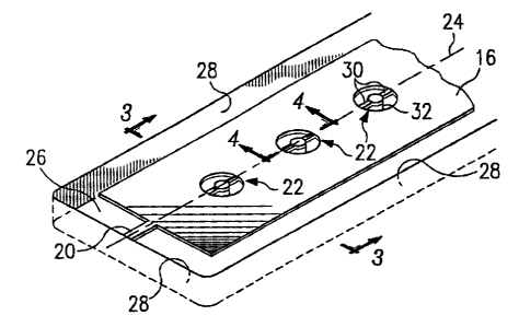
FIGURE 2 depicts perspectively the le~t half of the
mirror element 16 of Fiqure 1. It sh~uld be understood
that although only the le~t portion of mirror element 16
is depicted, a symmetrical right portion is intended.
Mirror element 16 is supported alonq its length by a
series of axially aligned supports. For stability
reasons, at least two supports must be used. These may
be either located at the end of mirror 16 as is hinge
element 20 or may be displaced from an edge of mirror
element 16 as are supporting members 22. All of the
supports are aligned along the line 24 ~orming the "axis
of rotation." These intermediat~ supporting members 22
stiffen mirror element 16 in the long di~ension without
impeding the rotation of mirror ele~ent 16 about its axis
o~ rotation. As a result, mirror element 16 is generally
planar with the top of well 26 or to the underlying
substrate. Each supporting ~ember is anchored to the
basQ of the well and insures the flatness o~ mirror
element 16 during operation. It should be understood
that well 26 ~ay, in ~act, be etched ~ro~ substrate 14 or
~ay simply remain after ~abrication o~ a layer or layers
which form sidewalls 28. Sidewalls 28 are generally
continuous around the perimeter of mirror element 16.
Without supporting member 22, mirror element 16
would sag into well 26 due to its relative great length
and thin cross section. In operation, mirror element 16
would not rotate about its axis of rstation 24 when
: ' - " ' '
,,, - .
, - :
2~8~9~
TI-16746 PATENT APPLIC~TIO`t
driven (as will be disc~ssed below) but might simply sag
downward ~urther if it is fabricated without supporting
member 22. Both of these results would interfere with
the desired light steering capabilities of the device.
Supporting member 22 itself comprises at least one hinge
element 30 which connect mirrsr elem~nt 16 to a central
post 32. In th~ pre~erred embodiment, supporting member
22 comprises two symmetrical hinye elem~nts 30. These
hinge members typically are made of the same material as
hinge element 20 and mirror element 16J ~
FIGURE 3 depicts mirror element 16 taken along line
3-3 of FIGURE 2. Mirror element l~ is supported by a
central post 32 in well 26. Central post 32 supports
mirror element 16 from the base of well 32 along the axis
of rotation 24. Device lO also contains at least one
electrode 34 displaced outwardly from th~ axis o~
rotation 24. A second complem~ntary ~lectrode 36 may be
added to device 10 in a second position also displaced
outwardly from the axis o~ rotation 24 and in a direction
generally opposite from the direction o~ electrode 34.
As depicted, electrodes 34 and 36 axa electrically
connected to a signal generator 37. Because mirror
element 16 and posts 32 can be el~ctrically isolated from
electrodes 34 and 36, an additional voltage can be
applied to the mirror ele~ent 16 itsel~ by ~i~nal
gen~rator 39 to accomplish other control functions well
known to the D~ u~er, such a bias and xesetO Signal
generators 37 and 39 may ~e located ~ithin or withou~
device 10.
Device lO might also compri~ ona or two stops 38
displaced outwardly ~xom ~lectrod~ 34 and 36 and held at
the same eleGtrical pot~ntial as ~irror ~le~ent 16.
Thes~ stops are called landing ~l~ctrode~ and are
positioned ~o that mirror ele~ent 16 will strike them
~s~ore striXing the electrodas 34 and 36 or any other
:: '
~I-16746 20~ ~ATE~JT APPLIC~TI~S
11
part of device 10. This prevents an electrical current
from flowing between mirror element 16 and the electrodes
34 and 36, or any other part, which would fuse ~he two
together or cause other damage. It should be understood
that the electrodes and stops may be single sets of small
pads, multiple sets of small pads or long strips running
generally parallel to the axis of rotation.
The periodic rotation of mirrsr element 16 about its
axis of rotation 24 may be controlled by applying an
alternating current between electrodes 34 and 36. The
signals applied to electrodes 34 and 36, in the preferred
embodiment, are 180- out of phas~ with each other and
have a frequency equal to the resonant frequency of
mirror element 16. Mirror element 16 is meanwhile held
at an intermediate potential. The a~plltude of rotation
may b~ regulated by controlling the amplitude of the
alternating waveform.
In the alternate, mirro~ 16 ~ay bQ driven of~
resonance. In such a case, it i~ deflected in an analog
~ashion to about 50% of the maximum rotation angle.
After that point, electrostatic ~ttraction, which goes as
the inverse square of the mirror 16 to eIectrode 34, 3
spacing, will overcom~ the lin~ar r~ torlng torgue of
hinges 30, and the mirror will land on landin~ electrode
38 at the ~ull daflection angle. This i. the digital
~ode o~ operation. The rate of rotation is controlled by
i~4Et~, I, and daMping due to the gas present in
the cavity 26 with the mirror.
` FIGURE 4 depicts a cross-s~ctio~al view o~ mirror
element 16 o~ FIGURE 2 taken along the lin~ 4-4. Here,
mirror elem~nt 16 is connected to support post 32 by two
thin hinge elements 30. Hinge ele~ents 30 are partially
covared by an oxid~ layer 40, a portion of which remains
a~ter manufacture as will b~ ~ore fully described below.
Cer.tral post 32 rests on ~lactrically isolatzd pad 42 and
,
-
2~
TI-16746 PATENT APPLIC~.T~5~i
layers 44 and 46. Substrate 46 ~ay contain circuitry
necessary to drive mirror element 16 about its axis of
rotation as described above.
FIGURES 5a-5f illustrate, in cross-sectional view,
sequential steps of the mirror element depicted in FIGURE
durins fabrication.
(a) Initially, substrate layer 46 is prepared using
conventional photolithographic technigues. Substrate
layer may contain, for instance, an internal oscillator
for driving mirror element 16 (FIGUREs 1-4) or other
control circuitry.
Each support post pad 42 is insulated from the
underlying substrate by an insulator such as silicon
dioxide layer 44, typically 2000 Angstro~s thick. Post
pad 42 is approximately 3000 Angstroms thick and is
fabricated from an alloy o~ aluminum, titanium, and
silicon ("Ti:Si:Al"). After the Ti:Si:Al is sputter
deposited onto silicon oxide layer 44, it is patterned
and plasma etch~d to define po~t pad 42, electrodes 34
and 36 and stops 38 (latter three shown in FIGURE 3).
(b) A photoresist is then spun on and baked in,
typically, three applications to a total ~hickness of
approximately 4 micron to for~ spacer 48. Three
applications o~, typically positiv~, resist are used to
2S fill the thicXnes~ to avoid re~ist sur~ac~ wave which
can occur when spinning on a single, ve n thick layer. A
bake o~ approximat~ly 180C i re~uired after ~ach
application o~ resist to prevent the pr~vious layers from
dissolving in subsequent resist applications, to drive
out excess solvent from the spaGer and to avoid the
formation of solvent bubbles under the hinge metal.
(c) Spacer 48 is etched to ~o~ a via that exposes
each post pad 42.
(d) Approximately 800 Angstroms of Ti:Si:Al is
applied to spacer ~8 to for~ p~rt o~ each post and a thin
.;
2~9~
TI~16746 PATENT APP~ICATI5~J
hinge layer 50 from which the end hinges and central
hinqes are etched. The resistancy to twist, or
flexibility of the hinges may ~e controlled by
controlling their length, width and thickness as well as
by controlling their composition. Typically, each hinge
is two microns wide. The support post hinges are ten
microns long. Next, 1,500 Angstroms of silicon dioxide
is deposited, patterned and etched to form hinge ~tch
stops 52 over all future hinges.
te) Approximately 3600 ~n~stroms of Ti:Si:Al is
sputter deposited onto hinge lay~er 50 and hinge etch
stops 52 to form mirror layer 54. The deposition of the
metal of mirror layer 54 is made under the same
conditions as ~or the deposition G~ hinge layer 50 so
that no stresses between the metal layers are developed.
The moment of inertia, I, of each mirror element 16
(shown in FIGUREs 1-4) may ba controlled by controlling
their length, width and thicknes as well as by
controlling their composition. Typically, each mirror
element is one quarter inch wid~ an~ onQ inch long.
Finally, an etch stop layer 56 i3 d~posited on top of
mirrox layar 54 ~or protection during subsequent
fabrication ~teps.
~f) A photore~ist layer is applied to etch stop
layer 56 and patterned to define plasma etch access holes
58 above hinge tops 52 (shown in ~IGURE 5e~. The
patterned photoræsist layer may ~hQn b~ llsed as a mask
for plasma etching the mirror element lay~r abovs each
hinge stop. Acces holes 58 appear as a 3et o~ "C's"
facing one another when viewed ~rom above. The plasma
Ptch of the aluminum alloy may be made with a
chlorine/boron trichlorideJcarbon trichloride etch gas
mixture. After the remaining photoresist layer is
removed, remaining etch stop layer 50 and the hinge etch
stops 52 may be xemoved by a~ anisotropic etch.
'' ' ' :
.
~I-16746 2 ~ 8 ~ NT APPLIC~
Access holes 58 may be minimized by making them
conform to the post and hinge dimensions, with a gap of
only 1 or 2 microns separating the posts and hinges from
mirror 16. This minimizes the optical effects of the
post and hinge features on the mirror per~ormance.
Spacer 48 is removed by, for instance, etching in
oxygen with a few percent fluorine. The completed
support post of the resonant mirror is depicted in FIGURE
4.
Optional end hinge 20 (depicted in FIGURE 2) i5
fabricated using the same steps as was the cantral pos~
and hinge elements depicted in FIGU~Es 5a-5f. Each end
hinge 20 is integrated into the surrounding of non-
rotating mirror metal. In some applications, it may be
preferable to eliminate the surrounding structure, so
. that only the active mirror element protrudes above the
substrate layer 46. Support posts could be provided at
mirror extreme ends in that case.
A practical limitation of the embodiment described
relates to the limiting ~pacer thickness and support post
heights achieva~le using reasonable se~iconductor
processe2. The size o~ the via ~ormad ln FIGU~E Sc is
related ~y technical process~ to ~h~ thickness of spacer
layer 48. In general, th~ thicker th2 spacer layer the
larger the subsequent via must ~o. Th~ size o~ the via
must be minimized, how~ver, to ~inimizQ any optical
ab~rrations in the resulting mirror el2ment 16. This
optical limitation, there~or, li~its ~he thickness of
spacer layer 48 and the maximum angle of rotation.
Spacer~ o~ the prescribed 4 micron thickness will only
permit rather small rotation angles for mirror~ having
any appreciable width. I~ a ~lO degree rotation angle is
desired, the width of the mirror can only be a f ctor of
12 times the thickness of ~he spacer layer 48 or abou~ 50
3S microns.
.
. ~ ~
TI-16746 2~ APPLICATI~J
FIGUREs 6 and 7 depict an asymmetric mirror
structure that overcomes the li~itation on rotation. It
can be operated only in one direction, but provides for a
relatively wide mirror and reasonable angles of operation
within the above spacer constraints.
FIGUREs 8 and 9 depict a practical way to achieve
lar~e ar~a mirrors, that can operate through angles of lO
degrees or greater, and meet tha ~anufacturing
constraints of spacer layer 48 and support posts 32. In
this approach, mirrors of large extent are seqmented into
a reticulated array of long slender el~ents 16. Each
mirror element 16 is supported on a line of supporting
elemPnts 22 as shown in FIGURE 3. Each mirror has the
electrode 34 and stop 38 structure depicted in FIGURE 3
necessary to address the mirror.
The optical e~fect of rotating ths array of elements
in synchroniæation about parallel axe~ 24 i5 equivalent
to rotating a larger mirror through the same angle. An
advantage of the retic~lated ~irror rotational scheme is
that the extrem~ end3 o~ th~ ~irror array remain in
approximately the sam~ plane a~ th~ center ele~e~ts.
Unlike the conventional macroscopic galvano~eter mirror,
which introduce3 chang~s in ~ho opt~cal path length as a
result o~ lts rotation about an axis p~rpendicular to the
optlcal path, the DMD ~irror array accompli~he~ b~am
~teering without changing th~ optical p~th length by more
thar. a ~ew micronsO While galvanometer~ re~ult in focus
changes and other optical artifacts, th~ reticulat~d
mirror ~ethod eliminates them~ Fresnell l~nses are
constructed on the same principle.
As a result of the ability to individually tilt the
long eleme~ts of the mirror array under precise
electrical control, the array can be used to ac~omplish
the same effect as a reflectiv~ Fre nell lens of a
cylindrical type (e.g. having optical power alon~ one
,
,, ;, ~ ~
~ '
2~8~
TI-16746 PATENT APPLIC~.~rO.
axis only, and no optical power along the orthogonal
axis). Signal generators 37 and 39 (shown in FIGURE 3)
may apply a prescribed series o~ voltage steps to the
address electrodes of the parallel rows o~ mirrors
corresponding to an equation describing the desired one
dimensional optical surface. For instance, a plane
mirror may be modeled by applying generally equivalent
voltage levels to each electrode. Other optical sur~aces
may be modeled by tilting the ~irrors a varying amount.
This would provide an active, electronically programmable
reflective, cylindrical optical element.
It is also possibl~ under control o~ signal
generators 37 and 39 to co~bine ~oth the ef~ect Or the
lens and th~ steering mirror. ~ight i~pinging on the
sur~ace could then be ~ocused and redirected at the same
time. This i5 possible due to the v~ry high rQsponse
speed of the DMD monolithic se~iconductor type ~irror
elements.
Altho~gh th~ prese~t lnve~tion ~a~ bean d~scribed in
d~tail, it should be und~rstood that various chang2s,
substltutions ~nd alteration~ can b~ ~ad~ hereto without
depart~ng ~ro~ the spirit and ~COpR ~S the invention as
de~i~ed by the appended Glaims.
' ' ~