Note: Descriptions are shown in the official language in which they were submitted.
FI9-90-0 18 1 ~ $
PROCESS AND STRUCTURE OF AN INTEGRATED
VACUUM MICROELECTRONIC DEVICE
Field Of The Invention
The present invention relates generally to a new integrated Vacuum Microelectronic Device
(VMD) and a method for making the same. Vacuum Microelectronic Devices require several unique
5 three dimensional structures: a sharp field emission tip, accurate alignment of the tip inside a control
grid structure in preferably a vacuum environment, and an anode to collect electrons emitted by the
tip.
Cross-Reference
This patent application relates to Canadian Patent Application Serial No. 2,085,982, filed
concurrently on October 17, 1990.
Background Of The Invention
The designers of electronic systems have for many years thought of ways to design and
improve semiconductor devices. The vacuum tube, once the mainstay of electronics, had limitations
such as the mechanically fabricated structures inside the glass
~ ' t
W092/02030
PCT/US90/05963
208~981
envelope preventing miniaturization and integration,
and the thermionic cathode keeping the power drain
high. There have recently been significant
developments in this area that offer the opportunity
of escaping the previous restraints. Semiconductor
fabrication techniques can now be used to develop
structures in microminiature form and integrate many
of them together. Combining these microminiature
structures with a field emission electron source one
can now produce microminiature vacuum tube structures
which do not require heated cathodes. These
structures being on the order of micrometers in size,
permit the integration of many devices on a single
substrate, just as many semiconductor devices are
produced on a single chip.
The Vacuum Microelectronic Devices presently in
use require several unique three-dimensional
structures, which include, a vacuum space, a sharp,
preferably less than 100 nm radius field emission
tip, and the accurate alignment of tip inside an
extraction/control electrode structure. Vacuum
Microelectronic Devices include a field-emission
cathode and add additional structures, such as, an
extension of the vacuum space, an anode opposite the
cathode tip, and there may or may not be additional
accurately aligned control electrodes placed between
the tip and the anode.
The field emission display elements that utilize
these Vacuum Microelectronic Devices use the basic
field emission structure and add additional
structures, such as, an extension of the vacuum
space, a phosphor surface opposite the cathode tip,
and additional electrodes to collect and/or control
the electron current. Groups of individual Vacuum
Microelectronic Devices and/or display elements can
W092/02030
PCT/US90/05963
2085981
~e electrically interconnected during fabrication to
form integrated circuits and/or displays.
Vacuum Microelectronic Devices have several
unique features. They are expected to have sub pico
second switching speeds and are thought by some to be
the fastest electronic devices possible. They will
operate at temperatures ranging from near absolute
zero to hundreds of degrees Celsius limited
principally by their materials of construction.
These structures can be made of almost any conductor
and insulator material. They are intrinsically
radiation hard. They are also very efficient because
control is by charge and not by current flow, and the
use of high field emitters eliminates the thermionic
emission heaters of traditional vacuum devices.
In U. S. Patent No. 4,721,885, and also in an
article published by I-or Brodie, "Physical
Considerations in Vacuum ~icroelectronics Devices",
IEEE Transactions on Electron Devices, Vol. 36, No.
11, pages 2641-2644 (November 1989), a field-emission
microtriode is described. The triode consists of a
metal cone attached to a metal or high-conductivity
semiconductor base electrode. The height of the cone
is given as "h", the radius of curvature at the
cathode tip is "r". A metal anode is held at a
distance "d" from the tip of the cone by a second
insulating layer. The cone tip is at the center of a
circular hole having a radius "a", in a gate (or
first anode) electrode of thickness "t". When the
appropriate pos~'ive potential difference is applied
between the base electrode and the gate electrode, an
electric field is generated at the cathode tip that
allows electrons to tunnel through the tip into the
vacuum space and move towards the anode. The field
W092/02030 PCT/US90/05963
2G8598~ ~
at the tip and, hence, the quantity of electrons
emitted can be controlled by varying the gate
potential.
While these Vacuum Microelectronic Devices can
be made in almost any size and may have applications
as discrete devices, their best performance and major
application is expected to come from extreme
miniaturization, large arrays, and complex very large
scale integration of circuits.
Non-thermionic field emitters, field emission
devices, and field emission displays are all known in
the art. Since the fabrication of the field emission
cathode structure is a critical element common to the
devices mentioned, its art will be addressed first.
The material (insulators and conductors/field
emitters) are all deposited and processed by
relatively common deposition and lithographic
processing techniques with the single exception of a
special sharp edge (blade) or point (tip) structure
which is common to all field-emission cathodes. The
art can be broadly classified into five categories,
and these categories are primarily categorized by the
methods used to form this sharp blade or tip.
The first category is one of the earliest
categories in which the cathode tip structure is
formed by the direct deposition of the material. An
example of this type is exemplified in a paper by C.
A. Spindt, "A Thin-Film Field-Emission Cathode", J.
Appl. Phys., Vol. 39, No. 7, pages 3504-3505 (1968),
in which sharp molybdenum cone-shaped emitters are
- formed inside holes in a molybdenum anode layer and
on a molybdenum cathode layer. The two layers are
separated by an insulating layer which has been
etched away in the areas of the holes in the anode
layer down to the cathode layer. The cones are
W O 92/02030
P(~r/US90/05963
2085981
formed by simultaneous normal and steep angle
depositions of the molybdenum and alumina,
respectively, onto the rotating substrate containing
the anode and cathode layers. The newly deposited
alumina is selectively removed. Similar work has
also been disclosed in U. S. Patent No. 3,755,704.
A second category is the use of
orientation-dependent etching of single crystal
materials such as silicon. The principle of the
orientation-dependent etching is to preferentially
attack a particular crystallographic face of a
material. By using single crystal materials
patterned with a masking material, the
anisotropically etched areas will be bounded by the
slow etching faces which intersect at well defined
edges and points of the material's basic
crystallographic shape. A suitable combination of
etch, material, and orientation can result in very
sharply defined points that can be used as field
emitters. U. S. Patent No. 3,665,241 issued to
Spindt, et al., is an example of this method in which
an etch mask of one or more islands is placed over a
single-crystal material which is then etched using an
etchant which attacks some of the crystallographic
planes of the material faster than the others
creating etch profiles bounded by the slow etching
planes (an orientation-dependent etch). As the slow
etching planes converge under the center of the mask,
multifaceted geometric forms with sharp edges and
points are formed whose shape is determined by the
etchant, orientation of the crystal, and shape of the
mask. Orientation-dependent anisotropic etching
while an established method to create the tips can
also have an adverse effect by making these sharp
tips blunt (or reducing the radius of the cathode
W092/02030
PCT/US90/05963
2085981
tip), thus redueing their effectiveness as field
emitters, as diseussed by Cade, N. A. et al., "Wet
Etehing of Cusp Struetures for Field-Emission
Deviees," IEEE Transactions on Electron Devices, Vol.
36, No. 11, pages 2709-2714- (November 1989).
A third category uses isotropic etches to form
the structure. Isotropic etches etch uniformly in
all directions. When masked, the mask edge beeomes
the eenter point of an are whieh outlines the classic
isotropie eteh profile under the masking material.
The radius of the arc is equal to the eteh depth.
Etehing around an isolated masked island allows the
eteh profile to eonverge on the eenter of the mask
leaving a sharp tip of the unetehed material whieh
ean be used as a field emitter. An example of this is
exemplified in U. S. Patent No. 3,998,678, issued to
Shigeo Fukase, et al. An emitter material is masked
using islands of a lithographieally formed and eteh
resistant material. The emitter material is etehed
with an isotropic etchant which forms an isotropic
etch profile (cireular vertical profile with a radius
extending under the resist from the edge). When the
eteh profile eonverges under the eenter of the mask
from all sides, a sharp point or tip results.
A fourth eategory uses oxidation proeesses to
form the Vaeuum Microelectronic Deviee. Oxidation
proeesses form a tip by oxidizing the emitter
material. Oxidation profiles under oxidation masks
are virtually identieal to isotropic etch profiles
under masks and form the same tip strueture as the
profiles eonverge under a eireular mask. When the
oxidized material is removed the unoxidized tip ean
function as a field emitter. U. S. Patcnt No.
3,970,887 issued to Smith et al. exemplifies this
process. A substrate of electron emission material
W O 92/02030
PC~r/US90/05963
2085381
such as silicon is used. A thermally grown oxide
layer is grown on the substrate and is then
lithographically featured and etched to result in one
or more islands of silicon dioxide. The substrate is
then reoxidized during which the islands of
previously formed oxide act to significantly retard
the oxidation of the silicon under them. The
resulting oxidation profile is very similar to the
isotropic etch profile and similarly converges under
the islands leaving a sharp point profile in the
silicon which can be exposed by removing the oxide.
Other masking material such as ~llicon nitride can be
used to similarly retard the oxidation and produce
the desired sharp tip profile.
A fifth category etches a pit which is the
inverse of the desired sharply pointed shape in an
expendable material which is used as a mold for the
emitter material and then removed by etching. U. S.
Patent No. 4,307,507 issued to Gray et al exemplifies
a limited embodiment of this technique. Holes in a
masking material are lithographically formed on a
single crystal silicon substrate. The substrate is
orientation-dependent etched through the mask holes
forming etch pits with the inverse of the desired
pointed shape. The mask is removed and a layer of
emission material is deposited over the surface
filling the pits. The silicon of the mold is then
etched away freeing the pointed replicas of the pits
whose sharp points can be used as field emitters.
All of the emitter formation techniques
mentioned above have several limitations.
Orientation-dependent etching requires the use of a
substrate of single crystal emitter material. Most
all of them require the substrate to be made of or
coated with the emitter material. Most all of them
W O 92/02030
PC~r/US90/05963
2085981 -
form the emitter first which complicates the
fabrication of the subsequent electrode layers and
the vacuum space needed for a fully functional Vacuum
Microelectronic Device.
Sometimes the method used or the particular
processing regime does not produce field emission
tips of sufficiently small radius. The art includes
some methods by which the tip can be sharpened to
further reduce this radius. In a paper by Campisi et
al, "Microfabrication Of Field Emission Devices For
Vacuum Integrated Circuits Using Orientation
Dependent Etching", Mat. Res. Soc. Symp. Proc., Vol.
76, pages 67-72 (1987), reports the sharpening of
silicon tips by slowly etching them in an isotropic
etch. Another paper entitled "A Progress Report On
The Livermore Miniature Vacuum Tube Project", by W.
J. Orvis et al, IEDM 89, pages 529-531 (1989),
reports the sharpening of silicon tips by thermally
oxidizing them and then etching away the oxide. U.
S. Patent No. 3,921,022, also discloses a novel
method of providing multiple tips or tiplets at the
tip of a conical or pyramidical shaped field emitter.
Various processes creating two or three
electrode VMD structures been reported in the art.
As an example a paper entitled "A Progress Report On
The Livermore Miniature Vacuum Tube Project", by
Orvis et al, IEDM, pages 529-531 (1989), describes a
process in which silicon emitters formed by either
orientation-dependent or isotropic etching are used.
Lithographically featured doped polysilicon anode and
grid layers are separated from the emitter and each
other by layers of low density glass.
It is now possible as exemplified in Busta, H.
H. et al. "Field Emission from Tungsten-Clad Silicon
Pyramids", IEEE Transactions on Electron Devices,
W092/02030
PCT/US90/05963
2085981
Vol. 36, No. 11, pages 2679-2685 (November 1989), to
use coating or cladding on these cathode tips or
pyramids to enhance or modify the cathode tip
properties.
In this developing field of Vacuum
Microelectronic Devices the art has also started to
show how these field emission cathodes and extraction
electrodes can be used in a practical application,
such as, in a display applications. U. S. Patent No.
10 4,857,799 issued to Spindt et al illustrates how a
substrate containing field emitters and extraction
electrodes can be joined to a separate transparent
window which contains anode conductors and phosphor
strips, all of which can work in concert to form a
color display. Another color display device using
vacuum microelectronic type structure was patented in
U. S. Patent No. 3,855,499.
This patent application also discloses an etch
process which can significantly reduce the unwanted
undercut for a Vacuum Microelectronic Device while
still allowing the formation of bridge structures.
In summary a typical field emission Vacuum
Microelectronic Devices are made up of a sharply
pointed cathode, surrounded by a control and/or
extraction electrode, and pointing toward an anode
surface. The cathode tip could have a point or a
blade profile. One of the key technologies in
fabricating these devices is the formation of the
sharp field emission (cathode) tip which has
30 preferably a radius on the order of 10 - 100 nm. The
most common methods of formation include
orientation-dependent etching, isotropic etching, and
thermal oxidation.
W092/02030
PCT/US~/05963
2o8s98l
--10--
SUMMARY AND OBJECTS OF THE I~Vhr.llON
In one aspect this invention discloses a process
of making at least one integrated vacuum
microelectronic device comprising the steps of:
5a) providing at least one hole in a substrate
having at least one electrically conductive material,
b) filling at least a portion of the hole with
at least one material sufficiently to form a cusp,
c) depositing at least one layer of a material
which is capable of emitting electrons under the
influence of an electrical field, and filling at
least a portion of the cusp to form a tip,
d) providing at least one access hole to help
facilitate the removal of material underneath the
cusp, and
e) removing the material underneath the cusp to
expose at least a portion of the tip of the
electron-emitting material and at least a portion of
the electrically conductive material in the
substrate, thereby forming at least one integrated
vacuum microelectronic device.
In another aspect this invention discloses a
process of making at least one integrated vacuum
microelectronic device comprising the steps of:
25a) providing at least one hole in a substrate,
b) depositing at least one insulative material
and filling the hole to form a cusp,
c) depositing at least one layer of a material
which is capable of emitting electrons under the
influence of an electrical field, and filling at
least a portion of the cusp to form a tip,
d) providing at least one access hole to help
facilitate the removal of material underneath the
W O 92/02030
PC~r/US90/05963
~ass~sl .
cusp, and
e) through the access hole removing all of the
material in the hole and exposing at least a portion
of the tip of the electron-emitting material and at
least a portion of the electrically conductive
material in the substrate, thereby forming at least
one integrated vacuum microelectronic device.
Still another aspect of this invention discloses
an integrated vacuum microelectronic device
comprising an electron-emitting material having a
field emission tip and at least one access hole that
leads into a chamber, wherein the field emitter tip
face an anode which is in the chamber and separated
by at least one material.
The integrated vacuum microelectronic device of
this invention could also have at least one emitter
tip which is electrically isolated from another tip
or at least one tip could be electrically connected
to another electronic component. Similarly, the
anode could be a part of an electronic display device
or the device itself could be a used in an electronic
display device.
A product can also be made by any of the
processes of this invention.
One object of this disclosure is to fabricate
one or more Vacuum Microelectronic Devices,
consisting of a field emitter tip aligned inside a
control electrode (gate) and diametrically opposed to
a electron collection electrode (anode~.
Another object is to modify the k~-~sic process to
create simpler diode structures which function
without gate structures.
Still another object is to add additional gate
structures to form more complex devices such as, for
W O 92/02030
PC~r/US90~05963
20~5981
example, tetrodes (two gates), pentodes (three
gates), to name a few.
Yet another object is to limit the nonproductive
undercut of this process by employing a novel two
step etching sequence.
Still yet another object of this invention is to
interconnect at least one of the VMD device into
integrated circuits.
Yet another object of this invention is to
interconnect at least one of the VMD device to
another electronic device.
The objects of the present invention can be
achieved using a novel fabrication process in which
the conformal deposition of an insulator into a hole
produces a symmetric cusp that can be used as a mold
to form a pointed or sharp field emission tip. Since
it is only the physical hole that allows the cusp to
form, the hole can be created out of any stable
material including layered alternating stacks of
conductors and insulators which can act as the
electrodes of the finished device. Two electrodes
(anode and emitter) form a simple diode while three,
four, and five electrodes would form respectively a
triode, tetrode, and pentode for example. Further,
since the cusp is self aligned within the center of
the hole it is also aligned to the center of these
electrodes. The basic device structure is completed
by filling the cusp with a material capable of
emitting electrons under the influence of an electric
field or an electron-emitting material. Access holes
created in the electron-emitting material allow the
removal of the insulator of the cusp forming layer
from the hole and from underneath the emitter
material, thus forming a space and freeing the sharp
tip of the emitter (field emission cathode) that was
W092/02030
PCT/US90/~963
208~981
molded by the cusp.
The process is not limited to any particular set
of emitter, conductor, or insulator materials. ~any
different materials and material combinations can
easily be used with this process.
The removal of the cusp insulator material to
produce a clean emitter tip, results in the removal
of material from under the emitter to free the tip,
requiring the use of for example an isotropic etch.
Exclusive use of isotropic etching would produce
excessive nonproductive undercut. This nonproductive
undercut only serves to weaken the structure and
occupy unnecessary space. To eliminate this
limitation a novel two step etch process is used to
minimize this nonproductive undercut. In this
process, two access holes, one on each side of the
emitter bridge that spans the vacuum space are made.
These access holes intentionally overlap the vacuum
space hole. These access holes further allow the
cusp insulator etchants to empty the vacuum space. A
reactive ion etch (RIE) is used to selectively etch
the insulator all the way to the bottom of the vacuum
space hole without undercut. A selective isotropic
etch (wet or plasma) is then used to remove the
insulator partition from under the bridge, thus
freeing the emitter tip and creating the opening for
the vacuum space or forming a chamber. The resulting
undercut on other exposed insulator edges is limited
to an amount equal to half the partition thickness
because it is being etched from both sides.
Since the electrodes are made of simple
conductors, device interconnection can be
accomplished using the same layers and vertically
through vias in the insulators. This eliminates the
extra wiring layers and greatly simplifies overall
W092/02030
PCT/US90/~963
2o8s9~l
fabrication, turnaround time, and device area by
reducing the average number of device contact
openings.
Passive devices are also easily made. For
example, capacitors can be made across the normal
insulating layers even allowing vertical coupling of
layers capacitively (e.g. one device's plate to
another's grid level) and can also be integràted in
substrate using trench techniques. The use of metal
oxides is a good example of resistor elements and it,
too, may be done between vertical conductor levels or
as separate elements.
Additional advantages and features will become
apparent as the subject invention becomes better
understood by reference to the following detailed
description when considered in conjunction with the
accompanying drawings.
BRIEF DESCRIPTION OF T~ DRAWINGS
The features of the invention believed to be
novel and the elements characteristic of the
invention are set forth with particularity in the
appended claims. The drawings are for illustration
only and are not drawn to scale. The invention
itself, however, both as to organization and method
of operation, may best be understood by reference to
the detailed description which follows taken in
conjunction with the accompanying drawings in which:
Figure lA, is a cross-sectional view of a base
of a VMD having an conductive layer over an
insulative substrate.
Figure lB, is a cross-sectional view of another
embodiment of a base of a VMD having an conductive
WO92/02030
PCT/US90/05963
2o8s98l -
layer, and an in insulator layer over a conductive
substrate.
Figure 2, sho~ a cross-sectional view of the
base of Figure lA having a grid insulator and a grid
conductor over it.
Figure 3, is a cross-sectional view with a
portion of the VMD structure etched.
Figure 4, is a cross-sectional view showing the
deposition of a cusp forming material.
Figure 5, is a cross-sectional view showing the
deposition of an electron-emitting material.
Figure 6, is a cross-sectional view showing the
access holes through the electron-emitting material.
Figure 7A, is a cross-sectional view of a
completed VMD triode as a result of an isotropic
etching.
Figure 7B, is a cross-sectional view of a VMD
triode as a result of an anisotropic etching.
Figure 8, is a cross-sectional view of a
completed VMD triode as a result of an isotropic
etching of the structure of Figure 7B.
Figure 9A, is a cross-sectional view of VMD
diode made according to the teachings of this
invention.
~igure 9B, is a cross-sectional view of another
embodiment of a VMD diode made according to the
teachings of this invention.
Figure 9C, is a cross-sectional view of still
another em~odiment of a VMD diode made according to
the teachings of this invention.
Figure 9D, is a cross-sectional view of yet
still another embodiment of a VMD diode made
according to the teachings of this invention.
Figure 10, is a cross-sectional view of a
completed pentode VMD made according to the teachings
WO92/02030
PCT/US90/05963
208S~81
-16-
of this invention.
DETAILED DESCRIPTION OF THE INVENTION
This invention describes a novel new technique
and structure for the integrated fabrication of one
or more integrated Vacuum Microelectronic Devices.
One of the major elements in the fabrication of
the integrated Vacuum Microelectronic Device is the
use of the cusp which is formed by the conformal
deposition in a round hole. Other symmetrical hole
shapes will also result in a single pointed cusp, but
a round shaped hole will result in an optimum cusp.
The layer made of conductive material could also
be made of composite layers of conductive material,
so that the tip ends up as being made of a layered or
composite material.
Once this template is etched away using
isotropic etch which simultaneously forms the vacuum
space, an emitter point will result. Preferably,
this tip should have the required small radius (for
example between 10-lOOnm), required by the device,
but if necessary, the tip can be further sharpened by
isotropic etching or oxidizing a small amount of the
conductor tip to achieve any desired tip radius.
It is important to note that many different com-
binations of materials, deposition techniques(sputter, CVD, plating, etc.), and etch techniques
(wet, dry, ion, etc.) or additive pattern formation
techniques can be used in the fabrication steps.
Another method of vertical integration is the
stacking of whole device layer sets one on top of
another. Since these devices are not dependent on
special materials such as single crystal silicon,
W O 92/02030
PC~r/US90/05963
208~981
these device layer sets can also be integrated on top
of other technologies such as semiconductors and
multilayer ceramic packages.
The detailed description of the Vacuum
Microelectronic Device structure and the process for
fabricating it, as described below, has been
simplified ~y using several predefined and named
process sequences or definitions that are
repetitively referenced.
The term VMD or Vacuum Microelectronic Device as
used herein, means not only a diode but a triode,
tetrode, pentode or any other device that is made
using this process, including the interconnection
thereof. Basically, a VMD is any device with at
least a sharp emitter (cathode) tip, and a collector
(anode) with an insulator separating the emitter and
there is a preferably a direct transmission of
electrons from the emitter to the collector.
The term "lithographically defined" refers to a
process sequence of the following process steps.
First a masking layer that is sensitive in a positive
or negative sense to some form of actinic radiation,
for example, light, E-beams, and/or X-rays, is
deposited on the surface of interest. Second, this
layer is exposed patternwise to the appropriate
actinic radiation and developed to selectively remove
the masking layer and expose the underlying surface
in the patterns required. Third the exposed surface
is etched to remove all or part of the underlying
material as required. Fourth, the remaining areas of
the masking layer are removed.
Alternatively, the term "lithographically
defined" can refer to following "liftoff process."
The same required patterns in a material layer as
produced in the previously described process are
W092/02030
PCT/US90/05963
2o~5981 ,
-18-
created. This process starts on the surface that is
to receive the desired patterned material layer.
First, a masking layer that is sensitive in a
positive or negative sense to some actinic radiation,
for example, light, E-beams, and/or X-rays, is
deposited on the surface. Secondly, this layer is
exposed patternwise to the appropriate actinic
radiation and developed to selectively remove the
masking layer and expose the underlying surface in
patterns where the desired material layer is to
remain. The deposition, exposure, and development
process is controlled in such a way that the edges of
the remaining mask image has a negative or undercut
profile. Thirdly, the desired material is deposited
over both the open and mask covered areas by a line
of sight deposition process such as evaporation.
Finally, the mask material is removed, for example,
by dissolution and freeing any material over it and
allowing it to be washed away.
The term "conductive material" or "conductor
layer" or "conductive substrate" refers to any of a
wide variety of materials which are electrical
conductors. Typical examples include the elements
Mo, W, Ta, Re, Pt, Au, Ag, Al, Cu, Nb, Ni, Cr, Ti,
Zr, and Hf, alloys or solid solutions containing two
or more of these elements, doped and undoped
semiconductors such as Si, Ge, or those commonly
known as III-V compounds, and non-semiconductinq
compounds such as various nitrides, borides, cubides
(for example LaB6), and some oxides (of for example
Sn, Ag, InSn).
The term "insulative material" or "insulator
layer" or "insulative substrate" refers to ~ wide
variety of of materials that are electrical
insulators especially glasses, and ceramics. Typical
W092/02030 PCT/US90/0~963
208~
-19-
examples include elements such as carbon in a diamond
form (crystalline or amorphous), single crystal
compounds such as sapphire, glasses and
polycrystalline or amorphous compounds such as some
oxides of Si, Al, Mg, and Ce, some fluorides of Ca,
and Mg, some carbides and nitrides of silicon, and
ceramics such as alumina or glass ceramic.
The term "electron-emitting material" or
"emitter layer" or "emitter material" refers to any
material capable of emitting electrons under the
influence of an electric field. Typical examples
include any of the electrical conductors, such as the
examples listed above, and borides of the rare earth
elements, solid solutions consisting of 1) a boride
of a rare earth or an alkaline earth (such as Ca, Sr,
or Ba), and 2) a boride of a transition metal (such
as Hf or Zr). The emitter material can be a single
layered, a composite or a multilayered structure. An
example of a multilayered emitter might include, the
addition of one or more of the following, a work
function enhancement layer, an robust emitter layer,
a sputter resistant layer, a high performance
electrically conductive layer, a thermally conductive
layer, a physically strengthening layer or a
stiffening layer. This multilayered composite may
contain both emitter and non-emitter materials, which
can all act synergistically together to optimize
emitter performance. An example of this is discussed
in Busta, H. H. et al. "Field Emission from
Tungsten-Clad Silicon Pyramids", IEEE Transactions on
Electron Devices, Vol. 36, No. 11, pages 2679-268~
(November 1989), where they show the use of coating
or cladding on these cathode tips or pyramids to
enhance or modify the cathode tip properties.
This coating or cladding can also be used in
W092/02030 PCT/US90/05963
208S981 '
-20-
situations where one cannot form the desired tip
structure or it is difficult to form the desired tip
structure for the cathode emitter.
The term "deposited" refers to any method of
layer formation that is suitable to the material as
are generally practiced throughout the semiconductor
industry. One or more of the following examples of
deposition techniques can be used with the previously
mentioned materials, such as, sputtering, chemical
vapor deposition, electro or electroless plating,
oxidation, evaporation, sublimation, plasma deposi-
tion, anodization, anodic deposition, molecular beam
deposition or photodeposition.
The term "tip" as used herein means not only a
pointed projection but also a blade. Field emitter
shapes other than points are sometimes used, such as
blades. Blades are formed using the same methods
except that the hole is a narrow elongated segment.
The shape of the sharp edge of the blade can be
linear or circular or a linear segment or a curved
segment to name a few.
The hole that is used to eventually form the
cusp, from the cusp forming material, can be formed
by a process selected from a group comprising,
ablation, drilling, etching, ion milling or molding.
The hole can also be etched, using etching techniques
selected from a group comprising anisotropic etching,
ion beam etching, isotropic etching, reactive ion
etching, plasma etching or wet etching. The hole
could have a profile where the dimensions of the hole
are constant with depth or the dimensions of the hole
could vary with depth.
The cusp forming material is preferably
conformally deposited. The cusp forming material
could be an insulative material or it could comprise~
W092/02030 PCT/US90/05963
208~981
-21-
of multilayers.
The access hole that is formed to remove the
material from underneath the electron-emitter tip
could be formed by a process selected from a group
comprising, ablation, drilling, etching or ion
milling. The access hole could also be etched, using
etching techniques selected from a group comprising
anisotropic etching, ion beam etching, isotropic
etching, reactive ion etching, plasma etching or wet
etching. Similarly, the material under the cusp
could be removed by a process selected from the group
comprising, dissolution or etching.
The substrate may be an insulator and serve as
part of the isolation between adjacent electrical
structures. Insulating substrates are especially
useful in minimizing parasitic capacitance which can
in turn significantly improve device frequency
response. Transparent insulating substrates are
especially useful in display applications where the
substrate can also serve as the display window on
which both light emitting structures and control
circuits can be integrated together.
The substrate could be made of a conductive
material. A conductive substrate may serve as part
of the functioning structure such as a common anode
(plate) or a common bias voltage conductor. A
conductive substrate can also be isolated from the
electrical devices with the simple addition of an
insulating layer.
The substrate whether made from a conductive
material or an insulative material serves primarily
as a physical support for subsequent functional
layers and processing.
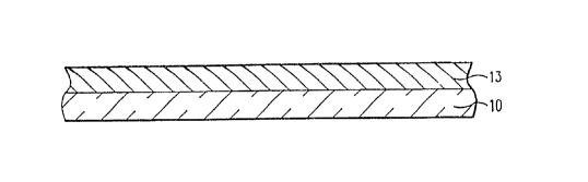
Figures lA and lB, illustrate the device base
structure. If the Vacuum Microelectronic Device, is
W092/02030 PCT/US~/05963
2~8~981
-22-
to be formed on an insulative substrate 10, then a
film or layer of conductive anode 13, is deposited
directly on the insulative substrate 10, as il-
lustrated in Figure lA. The insulative substrate 10,
could be made of a silicon dioxide material, but
other materials as discussed earlier can be used.
Doped polysilicon is a typical material for the anode
13, but other electrically conductive material as
discussed elsewhere could be used.
When a conductive substrate is used as a common
anode, or is a doped semiconductor material with any
desired isolations formed by electrically biased P-N
junctions, that substrate can be used directly. If,
a non-semiconductor conductive substrate (or a doped
semiconductor substrate without P-N junctions), is to
be isolated from the electrical devices, then an
insulating layer is deposited, followed by the
deposition of an anode conductive layer.
If an electrically isolatable VMD device is to
be formed on conductive substrate 11, as shown in
Figure lB, then on the conductive substrate 11, an
insulative film or layer 12 is deposited. A layer or
film of a conductive anode 13, which could be doped
polysilicon, is then deposited on the insulator layer
12. The material for the conductive substrate 11,
could be a silicon material. The insulative layer
12, can be formed by the oxidizing the silicon
material of the substrate 11, or be deposited by
other means known in the art. Other materials that
are equally acceptable for the conductive substrate
11 or the insulative layer 12, have already been
discussed earlier.
Once it is decided on the basic substrate
structure then the subsequent steps can be the same.
For the illustration of the best mode to carry out
W092/02030 PCT/US90/05963
2085~81
this invention the substrate configuration of Figure
lA, will be used, even though similar device would
result if the substrate configuration of Figure lB,
is used.
As shown in Figure 2, on the anode conductive
layer 13, a layer of grid insulator 15, could be made
for example, by oxidizing the doped polysilicon of
layer 13, or by depositing an insulating glass layer,
to name a few. On top of grid insulator 15, is
deposited a layer of grid conductor 17, by any of the
methods discussed earlier. The material for the grid
conductor 17, for example, could be doped polysilicon
but, other materials discussed elsewhere can also be
used.
This process of forming additional insulative or
conductive materials is repeated for each control
electrode structure desired in the final active
device.
The next step is to create the vacuum hole or
space 19, as shown in Figure 3. The vacuum space 19,
is lithographically defined and etched by methods
well known in the art. The shape of the etch vacuum
space 19, can be square, round, oval, etc. The
radius or half of the maximum cross-sectional width
of the etched vacuum space 19, should be smaller than
the thickness of the sum o~ the layers that are
deposited or formed above t anode grid conductor
17. Anisotropic reactive io. etching RIE (Reactive
Ion Etching) is the preferred etch method, but other
methods known in the art could also be used. The
vertical or near vertical hole walls have minimal
lateral etching. This keeps electrode holes small
and uniform and also minimizes the overall area
occupied by the device. This operation creates holes
through all of the control electrode conductor and
W092/02030 PCT/US90/05963
2085981
-24-
insulator layers and will ultimately provide the
vacuum spaces for each of the Vacuum Microelectronic
Devices. Etching is continued through the grid
conductive layer 17, and the grid insulator layer 15,
until at least a portion of the anode layer 13, is
exposed. The vacuum space 19, does not need to
extend all the way to the upper surface of the
conductive material or- anode 13, if any of the
left-over material of the grid material or insulator
15, will etch out in the subsequent vacuum space
etching. It should be noted that the base layer or
substrate that is used be of sufficient thickness to
allow for the proper formation of hole or vacuum
space 19.
As shown in Figure 4, an insulative layer 21, of
sufficient thickness is conformally deposited to
close the etch vacuum space 19, in Figure 3, and form
a cusp 23. The insulative layer 21, for the purpose
of illustration is a silicon dioxide material. The
insulative layer 21, can be formed, for example, by
conformal chemical vapor deposition (CVD) process.
Conformal CVD deposition is typically used but other
processes such as anodization, and even marginally
conformal processes such as sputtering can produce
acceptable results. Deposition is continued until the
sidewall coatings converge and close the vacuum space
hole 19, This convergence forms the symmetrical cusp
23, with a very fine convergence point at the bottom
which is self-aligned to the center of the vacuum
space hole 19.
An electron-emitting material or layer 25, is
deposited by any means that will allow the material
to fill the cusp 23. This deposition could be done
as shown in Figure 5, for example, by CVD,
evaporation, sublimation, sputtering, electroless
W092/020~ PCT/US90/05963
208~981
deposition, or plating. The electron-emitting layer
25, acts as a cathode during the operation of the
device, and the sharp tip 27, acts as the cathode
emitter. The electron-emitting material 25, could be
formed for example by using doped polysilicon or
tungsten, but other materials as discussed elsewhere
could also be used.
The emitter layer 25, is now lithographically
featured with one or more access holes 29 and 30,
exposing the insulator layer 21, as shown in Figure
6. Two or more holes per device are desirable to
improve etching access, and to control undercut as
will be explained below. The access hole(s) are
pos-~tioned to overlap the vacuum space hole 19,
partlally but not to overlap the cusp 23.
The insulator layer 21, is now selectively
etched completely out of the vacuum space 19, leaving
conductive layers 25, 17 and 13, intact. This leaves
a bridge 37, of emitter layer 25, spanning the newly
created vacuum space or hole or chamber 39, and
supporting the sharp emitter tip 27, above the
exposed anode 13. The selective etch can etch grid
insulator 15, without harm to the finished device.
The selective etch can be a single step isotropic
(wet or plasma) etch which will result in a finished
device 45, as shown in Fig. 7A.
Device 45 in Fig. 7A is a functionally
acceptable triode device with emitter tip 27,
self-aligned in grid electrode 17, and directly
opposed to anode 13. It does, however, exhibit
excessive nonfunctional undercut 40, which not only
weakens the device structure, but also enlarges the
device and adversely affects the circuit density.
A two-step etch process minimizes these
unnecessary attributes. A selective anisotropic etch
W092/02030 PCT/US90/05~3
208~981
-26-
is first used to etch, without undercut, layer 21,
all the way to the bottom of the vacuum hole 19, as
shown in Fig. 7B. This is possible because the
access holes 29 and 30, overlap the vacuum space or
S hole 19. This leaves only a thin partition or a web
31, under the emitter bridge 37, when two access
holes 29 and 30, one on each side of the bridge 37,
are used. A selective isotropic etch (wet or plasma)
is then used to remove the insulator partition 31,
from under the bridge 37, freeing the sharp emitter
tip 27, and completing the opening of vacuum space or
chamber 39, as shown in Figure 8. The resulting
undercut 41, on other exposed insulator edges, is
limited to an amount equal to half the thickness of
partition 31, because it is being etched from both
sides. The resulting finished device 50, is shown in
Fig. 8.
It must be remembered that the access holes 29
and 30, as shown in Figure 7B, are in two dimensions,
and that the etching to create access holes 29 and
30, was carried out using isolated holes, and
therefore both the partitions 31 and bridge 37, are
still a part of the insulating layer 21 and the
conductive layer 25, respectively.
The removal of the material under the bridge 37,
is usually the last operation done in order to mini-
mize contamination of that space or to avoid the
problem of removing future processing materials from
that confined area.
The sharp emitter tip 27, molded by the cusp 23,
can generally be controlled to have the desired small
radius tip without requiring further processing. If,
however, a smaller tip radius is desired or if a
particular set of desirable materials, pr~cess
techniques, and/or process conditions produce a
W092/02030
PCT/US90/05963
2Q8S981
-27-
larger then desired tip radius, then the tip can be
sharpened. This sharpening (the reduction of the tip
radius) can be done, for example, by slow etching of
the tip with an isotropic etch or the oxidation of
the tip followed by the removal of the oxide layer.
The process above, which results in triode
Vacuum Microelectronic Device 45 or 50, can easily be
adapted to form other configurations. In the figures
for the following examples the two step etch process
as used to remove layer 21, from hole 19, to create
vacuum space 39, as was used to produce triode device
50, will be illustrated.
Figures 9A, 9B, 9C, and 9D, illustrate a few
embodiments of a diode made according to the
teachings of this invention. An example of a diode
process sequence is created starting with the basic
triode process sequence through grid insulator 15.
The grid conductor layer 17, is eliminated. The
remaining process steps that would normally produce
triode 50, will now produce VMD diode 60, illustrated
in Fig. 9A. The phantom boundary of vacuum space
hole 19, would be solid if the selective etch for the
conformal layer 21, does not attack layer 15, or
would be lost as shown if it is attacked by the
selective etch process.
Figure 9B, shows the simplest form of a diode
structure that can be made by etching a vacuum hole
79, which is similar to the hole 19, directly into a
conductive substrate 11. The layer ll, must be
sufficiently thick to allow for the formation of the
hole 79. Starting with the deposition of the
conformal layer 21, the processing continues as
discussed earlier. A VMD diode 65, will result once
the process is completed as illustrated in Fig. 9B.
Similarly, a diode structure that can be
W O 92/02030 PC~r/US90/05963
208~981
-28-
produced on an insulative substrate 10, which has
been covered with the anode layer 13, is disclosed in
Figure 9C. The layer 13, must be sufficiently thick
to allow for the formation of the hole 79, which is
similar to the hole 19. The processing continues as
discussed earlier and upon completion, the result is
a VMD diode 70, as shown in Fig 9C.
Another embodiment of this invention is
illustrated in Figure 9D, where the insulative
substrate 10, is first featured with hole 79, and
then anode conductive material or layer 86, is
conformally deposited. The basic process starting
with the conformal deposition of insulator layer 21,
as discussed earlier is followed and the end result
is a VMD diode 75, as illustrated in Fig. 9D.
Many variations of more complex Vacuum
Microelectronic Devices can also be created by
extending the basic triode process. One example of
this variation is a VMD pentode device 90, as shown
in Fig. 10. The device 90, can be created from the
basic triode process sequence by following the basic
triode device sequence through the deposition of grid
conductor layer 17, then adding steps depositing grid
insulator 93, on grid conductor 17, depositing grid
conductor layer 94, on layer 93, depositing grid
insulator layer 95, on layer 94, and depositing grid
conductor layer 96, on layer 95. The basic triode
process is resumed at this step by creating hole 19.
In this case the hole 19, is etched through all the
layers until the upper surface of the conductive
material or layer 13, is exposed. If the basic
triode process sequence that would normally lead to
device 50, is followed from this point, it will
result in pentode device 90.
The insulator and conductor layers used above to
W092/02030 PCT/US90/05963
2085981
-29-
create the Vacuum Microelectronic Devices described
can also be used to isolate and interconnect multiple
electronic devices or components in three dimensions,
integrating circuits of these devices at the same
time that the devices are being fabricated. This is
not illustrated but can be accomplished by
lithographically patterning each conductive and
insulative layer after it is deposited and before
proceeding to the next step. Conductor material is
removed where isolations are desired and featured
into islands and paths to form interconnections
between different devices, between devices and vias,
and between different vias. Insulator layers can be
featured with a pattern of via openings to the
conductive layer below. Actual via connections may
be made either by the formation of a stud (a
conductive plug formed by a number of conventional
methods) or filled by the direct blanket deposition
of the next conductive layer thus creating vertical
interconnection pathways through the structure.
Any interconnection patterns created on the
emitter level can be made at the same time that the
access holes 29 and 30, are being made, but since the
insulator under them will be etched when the vacuum
space is etched the undercutting of these
interconnections represents a limitation on the size
of these features. The two step etch will
significantly minimize this undercut just as it does
in the device itself, but a further enhancement of
this process can eliminate undercut everywhere except
the vacuum device area. To accomplish this, a
separate or a second lithog~aphic step is used to
feature any emitter level isolations interconnections
and access holes. The second lithographic patterning
protects all of the interconnection and isolation
W092/02030 PCT/US90/~963
~08S981
-30-
features and exposes only the access holes. The
vacuum space etching which follows uses the two step
etch previously described and the small amount of
undercut that occurs is limited to the vacuum space
area only.
Many combinations of insulators and conductors
may be used in the fabrication procedures and device
structures described. Specific applications may
dictate special material properties such as
resistivity, dielectric constant, thermal stability,
physical strength, etc. but in general there are
three basic requirements for compatibility. First,
the materials must be compatible with the processing
required for fabrication which may limit some
material combinations in particular fabrication
regimes. Second, their must be adequate adhesion
between adjacent layers. Third, the materials must
be stable and not contaminate the operating
environment of the vacuum devices which is typically
a moderate to high vacuum. This last requirement is
somewhat open because some of these devices may be
able to operate in up to 1 atmosphere or more of a
high ionization potential gas such as He. This may
be possible because their microscopic dimensions
provide very small path lengths and allow the use of
low extraction voltages.
While the present invention has been
particularly described, in conjunction with a
specific preferred embodiment, it is evident that
many alternatives, modifications and variations will
be apparent to those skilled in the art in light of
the foregoing description. It is therefore
contemplated that the appended claims will ~mbrace
any such alternatives, modifications and variations
as falling within the true scope and spirit of the
W092/02030 PCT/US90/05963
20~5981
-31-
present invention.