Note: Descriptions are shown in the official language in which they were submitted.
~A ~~ ~ ~
Title: LASER-FORMED ELECTRICAL COMPONENT AND METHOD
FOR MAKING SAME
BACKGROUND OF THE INVENTION
The present invention relates to a laser-formed
electrical component and method for making same.
Specifically, the present invention relates to a
laminated electrical component comprising laminated
leyers of insulating material alternated with printed
patterns of helical coils formed from electrical
conductive material.
Many electrical components utilizing coils have
been manufactured in chip form, with various
alternating layers of ferrite material and conductors.
However, there are several disadvantages resulting
from the present methods for manufacturing these
devices. Most coils formed in this manner do not
include a complete coil having more than one
revolution at each laminated layer. Instead, present
devices place a portion of each coil on different
layers and connect these portions to provide a
completed coil having several turns.
Some present devices do place an entire coil
having more than one turn on each ferrite layer;
however, such devices are limited in their ability to
be miniaturized due to the limitations of the printing
techniques used. Present methods for forming the
conductive coils on each layer usually involve the
printing of the conductive material on the ferrite
layer. Most techniques for printing these layers do
not permit the lines to be much smaller than 8-10
mills., arid do not permit the spaces between the lines
,~°:..,
~4 r
20~01~~
- 2 -
to be much smaller than 8-10 mills. This minimum
dimension of the lines and spaces places a limit on
the amount of miniaturization which can be achieved
with coils of this type.
Lasers have been utilized in the resistor art for
trimming resistors, and for forming resistors.
However, the laser methods presently being used
involve the tracing with a lasex beam along the
particular pattern of conductor desired. This is a
time consuming task and does not permit the conductor
to be formed in a quick instantaneous fashion.
Therefore, a primary object of the present
invention is the provision of an improved laser-formed
electrical component and method for making same.
A further object of the present invention is the
provision of an improved laser-formed electrical
component which can be manufactured to smaller sizes
than prior art devices, while at the same time
achieving the same or greater inductance value than
presently available.
A further object of the present invention is the
provision of a method and means for making electrical
components which permits the width of the inductance
coil lines and the width of the spaces between the
inductor coil lines to be made smaller than in prior
devices.
A further object of the present invention is the
provision of a device and method which is economical
to use, efficient in operation, and reliable.
SUMMARY OF THE INVENTION
The present invention utilizes an Excimer laser
system which is capable of directing a burst of laser
208~~3~
- 3 -
energy through a mask assembly. The mask may be a
metal plate into which the desired pattern has been
cut. Acting like a stencil, the mask causes the image
of the desired pattern to be focused through a lens
onto a substrate having a layer of conductive material
thereon. The image burns away a portion of the
conductor layer, leaving the desired pattern such as a
coil or other electrical conductor path.
Inductor coils can be manufactured to include
alternating layers of ferrite material and conductor
coils. The conductor coils are formed by printing a
layer of conductive material such as silver on the
upper surface of a ferrite layer. The laser is then
used to project a negative image on the conductor
layer so as to remove the conductive material exposed
to the negative image. This leaves the conductive
coil formed on the upper surface of the ferrite layer.
Additional pairs of layers may be formed in the
same fashion and stacked upon one another to create a
stacked chip having a complete conductive coil having
more than one complete turn at each layer. Holes are
provided in the ferrite layers for connecting the
various conductive coils within the laminated chip in
series with one another to achieve the desired
inductance.
Excimer laser systems are presently available
which are capable of projecting an image over an area
from 5 to 10 square millimeters. This permits several
chips to be formulated at once. Thus, it is possible
to manufacture a single layer for a group of chips
with one single burst of the laser energy. The
individual layers are manufactured separately, and
then are stacked upon one another and fired so as to
2~861~~
- 4 -
form them into a single laminated group of layers.
Diamond saws are then used to cut the stacked layers
into individual chips.
BRIEF DESCRIPTION OF THE DRAWINGS
Figure 1 is a perspective view of the laser
system utilized with the present invention.
Figure 2 is a schematic view showing the manner
in which the laser system directs the laser beam onto
the work piece.
Figure 2a is a plan view of a mask utilized in
the present invention.
Figure 3 is a view showing the stacked multiple
chip layers which are formed by the present invention.
Figures 4a-4c are top plan views of a single chip
showing the first step in forming a first layer of
ferrite material and an electrical conductor coil.
Figures 5a-5c; 6a-6c; and 7a-7c are views similar
to Figures 4a-4c, and show the steps for forming
additional layer pairs for the laminated chip.
Figure 8 shows the final layer which is placed on
the laminated chip.
Figure 9 is a perspective view of a single
laminated chip, showing portions of the upper layer
cut away.
DESCRIPTION OF THE PREFERRED-EMBODIMENT
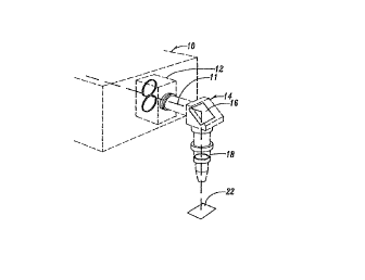
Figure 1 illustrates an Excimer laser system 10
which may be utilized for the present invention.
These systems are currently available for use in
marking and labeling electrical components. However,
these systems have not been utilized for the process
contemplated by the present invention. An example of
208138
- 5 -
such a system is manufactured by Lambda Physik, Inc.,
289 Great Road, Acton, Massachusetts 01720 under the
trademark "Lambda Mark".
The system generates a burst of laser light
designated by the line 11 in Figure 2. The laser
light 11 is directed first through a mask assembly 12
which includes a mask or stencil having the desired
pattern formed therein. After passing through the
mask, the laser is shaped into the image desired and
is deflected by mirror assembly 14 having mirror 16
therein downwardly through an imaging lens 18. Lens
18 can reduce the image several times so as to
intensify the image and provide greater focus to the
image. The image then is directed toward a work
surface 20 on which a work piece is placed. With
respect to the present invention, a mask 13 is
utilized which contains a coil negative pattern 15
therein. Pattern 15 is an opening through the mask 13
which is in the negative shape of the coil desired to
be formed. Thus, the resulting coil will ultimately
result in the form of the solid portion 17 shown in
Figure 2a.
Referring to Figure 3, a stack 22 of sheet
members 23, 24, 25, 26, 27 is shown. The top sheet
member 23 is made of a ferrite material commonly used
in the making of monolithic inductor chips. The
remaining sheet members 24-27 are also ferrite sheet
members, but include various printed conductive coils
28 thereon. The coils 28 on each sheet member are
identical to one another, but the coils are different
from one sheet member to another as will be explained
more fully hereinafter.
2(~86~.38
- 6 -
The dotted lines 30 represent cut lines which are
ultimately cut with a diamond saw to cut each of the
stacked members into individual chips containing one
set of coils 28. Figure 3 is drawn out of scale to
illustrate the various components of the invention.
However, in true scale, the layers 23-27 are paper
thin, and the lines of the coils 28 are approximately
mills wide with the spaces between the lines within
the coils also being approximately 5 mills.
The construction of each individual chip is
illustrated in Figures 4-8, but in actual practice the
layers for a plurality of chips are printed on each of
the ferrite layers 23-27 as shown in Figure 3. A
first ferrite layer 34 provides the bottom layer of
the chip. This ferrite layer 34 represents one of the
chips located in the multi-chip layer 27 shown in
Figure 3.
Figure 4b shows a first solid conductor layer 36
printed on the upper surface of ferrite layer 34.
Conductor 36 is preferably a silver material commonly
used in printed components of this type. Layer 36
includes a connector pad 38 which extends to the outer
margin of ferrite layer 34.
In Figure 4c, the completed conductive coil 40 is
shown. Conductive coil 40 is formed by exposing the
conductive layer 36 to a burst of laser light which
has first passed through mask 13 and then has been
reflected downwardly by mirror 16 through lens 18.
Thus, the negative image pattern 15 is focused on the
conductive layer 36 and burns away portions of the
layer 36 so as to leave the conductive coil 40 as
shown in Figure 4c. Coil 40 includes a center pad 42.
20~~1~8
_ 7 _
It should be noted that conductive coil 40
includes at least two complete turns of the coil on
one surface. Furthermore, the width of the conductor
40 can be as small as 5 mills, with the spaces between
the conductor coils being approximately 5 mills. This
is substantially smaller than is normally achieved
with prior devices, and it permits a maximum amount of
inductance to be achieved within a minimum of space.
An example of a preferred method for producing
the conductive coil 40 shown in Figure 4c is as
follows:
An Excimer laser system 10 such as the system
manufactured by Lambda Physik, Inc., 289 Great Rd.,
Acton, Massachusetts 01720, under the Trademark
"Lambda Mark", is used to produce conductive coil 40.
This particular machine includes several set up
parameters which can be set to produce the desired
result. The factors in these parameters are as
follows:
1. Various surface materials for the conductive
layer 36 produce different results.
2. The character size of the chip is a variable.
3. The character size of the stencil in the mask
is a variable.
4. The reduction ratio in the mask holder
assembly is a setting on the machine, which is
variable.
5. The focusing lens used by the machine, and
its micrometer location are variables.
6. The laser power setting, which is the DC
voltage setting on the system is another variable.
An example of a preferred setting of the system
is as follows:
208~~38
_8_
1. Surface material: unfired silver palladium
ink, manufactured by DuPont under the product
designation 7711.
2. The character or pattern size: .050 inches
square to .064 inches square.
3. The pattern size in mask: .500 inches
square.
4. The reduction ratio: between 10:1 and 7.8:1.
5. Focusing lens and micrometer location: SPLF
2010 lens set at a 56 centimeter position.
6. A laser power setting: 8.8 to 7.5 DC volts.
The system is then actuated to create a pulse of laser
light which is exposed to the layer 36 and which burns
away a coil 40, as shown in Figure 4c. The length of
time of exposer is estimated to be between .5
milliseconds and 2 milliseconds. However, the exact
amount of time cannot be determined with accuracy,
since the system utilized produces a capacitor
discharge for producing the light, and the specific
length of time of light exposure is not determinable
with accuracy.
Other systems may be utilized to produce the same
result, and other settings may also utilized to
produce different types of electrical components.
Figures 5a, b, and c illustrate the second
laminated layer which is formed by utilizing ferrite
sheet 44. The individual chip includes a second
ferrite layer 44 having an aperture 46 in the center
thereof which is in alignment above the center pad 42
of the first conductive coil 40. A second conductive
layer 48 is printed over the ferrite layer 44, and the
desired image is passed through a mask similar to that
shown in Figure 2a. However, the particular format
20~~~38
_ g _
for the mask is shaped so as to produce the second
conductive coil pattern 50 shown in Figure 5c. Coil
pattern 50 includes a second center pad 51 which is in
vertical alignment with aperture 46 and includes a
second end pad 52. The conductive material at the
center pad 51 protrudes downwardly through the
aperture 46 so as to make electrical contact with
center pad 42 of coil 40. This. electrically connects
coils 40 and 50 in series with one another.
Figures 6a-6c show a third laminated layer
comprising a third ferrite layer 53 having a connector
hole 54 therein; a third conductive layer 56, and a
third conductive coil 58 which is formed by a focused
laser image similar to the manner in which coils 40
and 50 are formed. The aperture 54 permits the third
end pad 62 of coil 58 to be connected to the end pad
52 of coil 50, thereby placing coils 40, 50, and 58 in
series with one another. Coil 58 includes a center
pad 60.
Figures 7a-7c show a fourth laminated layer
having a fourth ferrite layer 64 with an aperture 66
therein; a printed conductive layer 68 having an end
pad 74 thereon; and a fourth conductive coil 70 having
a center pad 72 thereon. Coil 70 is formed by a
focused laser image in similar fashion to the method
used for forming coils 40, 50, and 58. The center pad
72 protrudes through aperture 66 so as to form
electrical contact with center pad 60 of third
conductive coil 58. This places all four of the coils
40, 50, 58, and 70 in series with one another.
A final ferrite layer 76 is placed over the
laminated pad, so as to provide the configuration
shown in Figure 9.
208~:~38
- i0 -
The chip 78 shown in Figure 9 comprises one of
the plurality of chips which are formed by cutting
along the dotted lines 30 of the stack of sheet
members 23-27 in Figure 3. The ferrite layers 34, 44,
53, 64, and 76 are formed from the sheet members 27,
26, 25, 24, and 23 respectively of Figure 3. The
sheet members 23-27 are formed individually and then
are placed together in stacked fashion such as shown
in Figure 3. Specifically, the method of the present
invention contemplates printing each layer 23-27
individually by printing the conductive layers 36, 48,
56, and 68 thereon. The printed conductors are then
permitted to dry. Next, the printed conductors are
exposed to the images from the laser system 10. Each
sheet member 23-27 is individually exposed, but each
sheet member includes a plurality of identical sub-
parts. After the sheet members 23-27 have been
exposed to the image to form the coils 40, 50, 58, and
70, the sheet members 23-27 are stacked in the manner
shown in Figure 3 and are pressed together. While
being pressed, they are fired so as to cause them to
join together into a single unit.
After firing, the laminated sheet members 23-27
are then cut by a diamond saw along the lines 30 so as
to form individual stacked chips such as chip 78.
The present invention permits the chips to be
miniaturized more than in prior art devices. Because
the chips are miniaturized, more than one complete
turn of the coil can be placed on each layer; whereas,
with prior art devices, it was necessary to place less
than a complete turn on each layer. The coils of the
present invention can be miniaturized to the point
where the conductors have a width of approximately 5
- 11 -
mills with the spacing within the coil also being
approximately 5 mills wide. As many stacks as needed
can be provided in the chip, or the chip can be
comprised of only one coil and one layer. Because the
laser image is reduced down, the laser cut can be many
times smaller than that made by screen printing, and
the corresponding inductance values can be much larger
than presently available. Thus it can be seen that
the device accomplishes at least all of its stated
objectives.