Language selection

Search

Patent 2086367 Summary

Third-party information liability

Some of the information on this Web page has been provided by external sources. The Government of Canada is not responsible for the accuracy, reliability or currency of the information supplied by external sources. Users wishing to rely upon this information should consult directly with the source of the information. Content provided by external sources is not subject to official languages, privacy and accessibility requirements.

Claims and Abstract availability

Any discrepancies in the text and image of the Claims and Abstract are due to differing posting times. Text of the Claims and Abstract are posted:

  • At the time the application is open to public inspection;
  • At the time of issue of the patent (grant).
(12) Patent: (11) CA 2086367
(54) English Title: BONDING TOOL AND ITS FABRICATION
(54) French Title: DISPOSITIF DE SOUDAGE PAR THERMOCOMPRESSION
Status: Deemed expired
Bibliographic Data
(51) International Patent Classification (IPC):
  • H01L 21/70 (2006.01)
  • B23K 20/02 (2006.01)
  • H01L 21/603 (2006.01)
  • B23H 9/00 (2006.01)
(72) Inventors :
  • HORTON, RALPH M. (United States of America)
  • HOGGINS, JAMES T. (United States of America)
  • KUO, SHIH-YEE (United States of America)
(73) Owners :
  • NORTON COMPANY (United States of America)
(71) Applicants :
(74) Agent: GOWLING WLG (CANADA) LLP
(74) Associate agent:
(45) Issued: 2000-02-22
(22) Filed Date: 1992-12-29
(41) Open to Public Inspection: 1993-07-11
Examination requested: 1994-02-01
Availability of licence: N/A
(25) Language of filing: English

Patent Cooperation Treaty (PCT): No

(30) Application Priority Data:
Application No. Country/Territory Date
819,321 United States of America 1992-01-10

Abstracts

English Abstract


The disclosure is directed to a bonding tool for use
primarily in thermo-compression bonding of electronic circuit
components and to a method of making the bonding tool. In one
form of the disclosure, a holder is provided and has a substrate
mounted at an end thereof. The holder is adapted to receive a
heating element. A polycrystalline diamond film is disposed on
the substrate, the film preferably being deposited by chemical
vapor deposition. In a disclosed embodiment the substrate is a
material selected from the group consisting of polycrystalline
diamond, cemented tungsten carbide, silicon carbide, cubic boron
nitride, and tungsten. In a further form of the disclosure, a
ceramic substrate is provided which has a favorable thermal
conductivity property as well as substantial electrical
conductivity sufficient to permit shaping by electrical discharge
machining ("EDM").


Claims

Note: Claims are shown in the official language in which they were submitted.


CLAIMS:
1. A bonding tool, comprising:
a holder having a substrate mounted at an end thereof, said
substrate comprising a compact of polycrystalline diamond
particles;
a polycrystalline diamond film disposed on said substrate to
form a tip; and
means for coupling said substrate to a source for heating.
2. The bonding tool as defined by claim 1, wherein said
diamond film is a film deposited by chemical vapor deposition.
3. The bonding tool as defined by claim 1, wherein said
substrate is a material selected from the group consisting of
polycrystalline diamond, cemented tungsten carbide, silicon
carbide, cubic boron nitride, and tungsten.
4. The bonding tool as defined by claim 2, wherein said
substrate is a material selected from the group consisting of
polycrystalline diamond, cemented tungsten carbide, silicon
carbide, cubic boron nitride, and tungsten.
5. The bonding tool as defined by claim 1, wherein said
substrate comprises a compact of polycrystalline diamond
particles, and said diamond film is deposited on said compact.
6. The bonding tool as defined by claim 5, wherein said
diamond film is a film deposited by chemical vapor deposition.
7. The bonding tool as defined by claim 1, wherein said
holder includes a shank portion, a head portion, and an insert
connected to said head portion, said substrate being coupled with
said insert.
11


8. The bonding tool as defined by claim 3, wherein said
holder includes a shank portion, a head portion, and an insert
connected to said head portion, said substrate being coupled with
said insert.
9. The bonding tool as defined by claim 5, wherein said
holder includes a shank portion, a head portion, and an insert
connected to said head portion, said substrate being coupled with
said insert.
10. A method of forming a bonding tool, comprising the
steps of:
providing a substrate formed of polycrystalline diamond
particles;
depositing a film of polycrystalline diamond on a
surface of said substrate; and
mounting said substrate in a holder coupleable to a
heating element.
11. The method as defined by claim 10, wherein said step of
mounting substrate comprises mounting said substrate in an insert
portion of said holder.
12. The method as defined by claim 10, wherein said step of
depositing a diamond film comprises depositing a diamond film by
chemical vapor deposition.
13. The method as defined by claim 11, wherein said step of
depositing a diamond film comprises depositing a diamond film by
chemical vapor deposition.
14. The method as defined by claim 10, wherein said step of
depositing a diamond film comprises depositing a diamond film by
12


chemical vapor deposition with a plasma.
15. A method of forming a bonding tool, comprising the
steps of:
providing a substrate formed of a material selected
from the group consisting of polycrystalline diamond, cemented
tungsten carbide, silicon carbide, cubic boron nitride, and
tungsten;
shaping the substrate by electrical discharge
machining;
depositing a film of polycrystalline diamond on a
surface of said substrate; and
mounting said substrate in a holder coupleable to a
heating element.
16. The method as defined by claim 15, wherein said step
of mounting substrate comprises mounting said substrate in an
insert portion of said holder.
17. The method as defined by claim 15, wherein said step
of depositing a diamond film comprises depositing a diamond film
by chemical vapor deposition.
18. The method as defined by claim 16, wherein said step
of depositing a diamond film comprises depositing a diamond film
by chemical vapor deposition.
19. The method as defined by claim 15, wherein said step
of depositing a diamond film comprises depositing a diamond film
by chemical vapor deposition with a plasma.
20. A bonding tool, comprising:
a holder having a tip mounted at an end thereof, said
holder including means for receiving a heating element;
said tip comprising a ceramic material having an
13


electrical resistivity of less than 1000 ohm-cm and a thermal
conductivity of at least 60 W(m~°K)-1.
21. The bonding tool as defined by claim 20, wherein said
tip comprises a material selected from the group consisting of:
silicon carbide sintered with titanium diboride; aluminum nitride
doped with at least one dopant selected from yttrium oxide,
calcium oxide, dysprosium oxide, and ytterbium oxide; and silicon
carbide doped with at least one dopant selected from beryllium
and beryllium oxide.
22. A bonding tool, comprising:
a holder having a substrate mounted at an end thereof,
said holder including means for receiving a heating element; and
a tip disposed on said substrate;
said substrate comprising a ceramic material having an
electrical resistivity of less than 1000 ohm-cm and a thermal
conductivity of at least 60 W(m~°K)-1.
23. The bonding tool as defined by claim 22, wherein said
tip comprises a material selected from the group consisting of:
silicon carbide sintered with titanium diboride; aluminum nitride
doped with at least one dopant selected from yttrium oxide,
calcium oxide, dysprosium oxide, and ytterbium oxide; and silicon
carbide doped with at least one dopant selected from beryllium
and beryllium oxide.
24. The bonding tool as defined by claim 22, wherein said
tip comprises a polycrystalline diamond film deposited on said
substrate.
25. The bonding tool as defined by claim 23, wherein said
tip comprises a polycrystalline diamond film deposited on said
14


substrate.
26. The bonding tool as defined by claim 24, wherein said
diamond film is a film deposited by chemical vapor deposition.
27. The bonding tool as defined by claim 25, wherein said
diamond film is a film deposited by chemical vapor deposition.
28. A bonding tool, comprising:
a holder having a tip mounted at an end thereof, said
holder including means for receiving a heating element;
said tip comprising a ceramic material selected from
the group consisting of: silicon carbide sintered with titanium
diboride; aluminum nitride doped with at least one dopant
selected from yttrium oxide, calcium oxide, dysprosium oxide, and
ytterbium oxide; and silicon carbide doped with at least one
dopant selected from beryllium and beryllium oxide.
29. A bonding tool, comprising:
a holder having a substrate mounted at an end thereof,
said holder including means for receiving a heating element; and
a tip disposed on said substrate;
said substrate comprising a ceramic material selected
from the group consisting of: silicon carbide sintered with
titanium diboride; aluminum nitride doped with at least one
dopant selected from yttrium oxide, calcium oxide, dysprosium
oxide, and ytterbium oxide; and silicon carbide doped with at
least one dopant selected from beryllium and beryllium oxide.
30. The bonding tool as defined by claim 29, wherein said
tip comprises a polycrystalline diamond film deposited on said
substrate.


31. The bonding tool as defined by claim 30, wherein said
diamond film is a film deposited by chemical vapor deposition.
32. A method for making a bonding tool, comprising the
steps of:
providing a ceramic substrate having an electrical
resistivity of less than 1000 ohm-cm and a thermal conductivity
of a t least 60 W(m~°K)-1;
electrical discharge machining a surface of said
substrate into a predetermined shape; and
mounting said substrate on a holder.
33. The method as defined by claim 32, further comprising
the step of depositing a tip on said substrate.
34. The method as defined by claim 33, wherein said step of
depositing a tip comprises depositing a film which substantially
conforms in shape to said predetermined shape.
35. The method as defined by claim 33, wherein said step of
depositing a tip comprises depositing a diamond film on said
substrate.
36. The method as defined by claim 34, wherein said step of
depositing a tip comprises depositing a diamond film on said
substrate.
37. The method as defined by claim 35, wherein said step of
depositing a diamond film comprises depositing a diamond film by
chemical vapor deposition.
38. The method as defined by claim 36, wherein said step of
depositing a diamond film comprises depositing a diamond film by
16


chemical vapor deposition.
39. A method for making a bonding tool, comprising the
steps of:
providing a ceramic substrate comprising a ceramic
material selected from the group consisting of: silicon carbide
sintered with titanium diboride; aluminum nitride doped with at
least one dopant selected from yttrium oxide, calcium oxide,
dysprosium oxide, and ytterbium oxide; and silicon carbide doped
with at least one dopant selected from beryllium and beryllium
oxide;
electrical discharge machining a surface of said
substrate into a predetermined shape; and
mounting said substrate on a holder.
40. The method as defined by claim 39, further comprising
the step of depositing a tip on said substrate.
41. The method as defined by claim 40, wherein said step of
depositing a tip comprises depositing a film which substantially
conforms in shape to said predetermined shape.
42. The method as defined by claim 40, wherein said step of
depositing a tip comprises depositing a diamond film on said
substrate.
43. The method as defined by claim 41, wherein said step of
depositing a tip comprises depositing a diamond film on said
substrate.
44. The method as defined by claim 42, wherein said step of
depositing a diamond film comprises depositing a diamond film by
chemical vapor deposition.
17


45. The method as defined by claim 43, wherein said step
of depositing a diamond film comprises depositing a diamond film
by chemical vapor deposition.
46. A bonding tool, comprising:
a holder having a substrate the material of which has
a resistivity of less than 1,000 ohm centimeters, said substrate
being machinable by electrical discharge machining and mounted
at an end of said holder;
a polycrystalline diamond film disposed on said
substrate to form a tip; and
means for coupling said substrate to a source for
heating.
47. The bonding tool as defined by claim 46, wherein said
diamond film is a film deposited by chemical vapor deposition.
48. The bonding tool as defined by claim 46, wherein said
substrate is a material selected from the group consisting of
polycrystalline diamond, cemented tungsten carbide, silicon
carbide, cubic boron nitride, and tungsten.
49. The bonding tool as defined by claim 47, wherein said
substrate is a material selected from the group consisting of
polycrystalline diamond, cemented tungsten carbide, silicon
carbide, cubic boron nitride, and tungsten.
50. The bonding tool as defined by claim 46, wherein said
substrate comprises a compact of polycrystalline diamond
particles, and said diamond film is deposited on said compact.
18

Description

Note: Descriptions are shown in the official language in which they were submitted.


1
2086367
DF-2244
BONDING TOOL AND ITS FABRICATION
FIELD OF THE INVENTION
This invention relates to bonding tools and their
fabrication and, more particularly, to bonding tools used in the
production of electronic circuits, such as in thermocompression
bonding. of leads to integrated circuit devices or chips.
BACKGROUND OF THE INVENTION
During the assembly of electronic circuits, such as
integrated circuit chips, lead wires are bonded to contact pads
on a chip in an automated operation that uses a bonding tool
called a thermode. The leads may be in a machine-fed tape, and
the bonding tool, heated with a heating element, is automatically
pressed on the leads for a predetermined time to bond the leads
to the pads. The temperature of the banding tocl tip, and the
force it applies, results in the desired bond. The tool is then
lifted, the next set of parts is moved into position, and the
operation is repeated.
The bonding operation is preferably performed as quickly as
possible to prevent unwanted heating of the chip, to minimize
sticking between the tool tip and the leads, and to increase
production speed. The tip of the bonding tool must be brought to
an elevated temperature, and as it loses heat during each bonding
cycle it must quickly be returned to the desired temperature for
the next cycle. The bonding tool tip is also subjected to large
compressive forces, so the structure thereof must be able to
withstand such forces, without deforming or breaking, for many
thousands of operating cycles. Materials such as titanium
carbide and cubic boron nitride have been commonly employed as
1


_) _
.
_. r 208636
DF-2244
the tips of bonding tools.
The properties needed for a good bonding tool include
excellent heat conductivity, strength, stiffness, and low
coefficient of thermal expansion. Diamond, possessing these
properties, has accordingly been used as the tip of lead bonding
tools. In one prior art bonding tool design, a natural diamond
is mounted in a metal matrix, such as a tungsten powder, that is
held in an Inconel shank. A metal binder, such as silver or
copper alloy, covers the diamond. The assembly is heated in a
furnace to melt the binder, which infiltrates the matrix. Upon
cooling, the binder solidifies, consolidates the matrix, and
secures the diamond in place. The diamond is then machined, such
as by grinding, into a desired tip shape. In another prior art
approach, a diamond is pre-shaped into a desired tip
configuration and then brazed to an Inconel shank which may
optionally have an insert, such as of molybdenum. The cost of
natural diamond, and the difficulty of securing it and forming it
into a desired shape, are clear disadvantages of these types of
bonding tools.
Kerschner et al., IEEE Transactions On Components, Hybrids,
and Manufacturing Technology, Vol. CHMT-2 NO. 3, 1979, disclose a
thermode having a diamond tip attached to an*Inconel body. The
diamond tip contains a laser machined cavity to accommodate
devices to be bonded.
EPA Publication No. 032,437 discloses a thermocompression
bonding tool having a tip formed of a mass of synthetic
polycrystalline diamond material sintered in a predetermined form
and mounted on a cemented tungsten carbide substrate.
U.S. Patent No. 4,932,582 discloses a method for preparation
of a bonding tool. The superhard material of the tool can be
single crystal diamond, diamond compacts, CBN compacts, cemented
carbides, molybdenum and the like, and unified bodies of mixtures
thereof. Reference is also made in this patent to prior art
*Trade-mark
2


. . .)
2086367
DF-2244
bonding tools using sintered metal powders holding a single
crystal diamond head, and brazing of single crystal diamond to
tungsten or molybdenum shanks.
U.S. Patent No. 4,943,488 discloses a thermode which
includes a "TSPCD" (temperature stable polycrystalline diamond)
element bonded to a support or to an insert to be received in a
support.
Although the described approaches have advanced the thermode
art, there is substantial room for improvement in one or more of
the following areas:
The use of sintered diamond compacts as a tip can result in
thermally unstable structures and/or the presence of impurities
which can cause sticking or other operational problems.
The forming of extremely hard thermode tips into the variety
of shapes needed for different bonding jobs tends to be difficult
and/or expensive.
Adherence of the thermode tip to a holder or to a substrate,
and/or adherence of the substrate to a holder, may be inadequate
for long term use.
The thermal conductivity, stiffness, and/or coefficient of
expansion of the tip, substrate, and/or other portion of the
holder may limit the efficiency of the bonding. tool.
It is among the objects of the present invention to address
these and other limitations of the prior art in the fabrication
and structure of thermocompression bonding tools.
3


268636'
DF-2244
SUMMARY OF THE INVENTION
The present invention is directed to a bonding tool or
thermode for use primarily in thermo-compression bonding of
electronic circuit components and to a method of making the
bonding tool. In one form of the invention, a holder is provided
and has a substrate mounted at an end thereof. The holder
includes means for receiving a heating element. A
polycrystalline diamond film is disposed on the substrate, the
film preferably being deposited by chemical vapor deposition. In
a disclosed embodiment the substrate is a material selected from
the group consisting of polycrystalline diamond, cemented
tungsten carbide, silicon carbide, cubic boron nitride, and
tungsten. In this embodiment, the diamond film is deposited on
1~ the substrate using a plasma deposition technique.
A diamond film has a number of advantages for use as a
thermode tip. In addition to the recognized advantageous
properties of the diamond substance [including its thermal
conductivity, rigidity, long life, and resistance to wetting],
the diamond film can be deposited on surfaces having
predetermined shapes to avoid the difficulty of machining diamond
to obtain different thermode tip configurations as in the case of
natural diamond. Deposition of the diamond film on a
polycrystalline diamond substrate, such as a sintered diamond
substrate, is particularly advantageous. A diamond substrate
facilitates the deposition growth of a diamond film of desirable
quality. Further, the diamond film surface prevents substances,
such as cobalt or other metals or impurities in the underlying
substrate, from contaminating parts being bonded or causing
undesired sticking. Also, the relatively close matching of the
coefficient of expansion of the diamond film to that of the
diamond substrate enhances the temperature performance and
longevity of the bonding tool.
4


2086367 DF-2244
In accordance with a further form of the invention, a
ceramic substrate is provided which has a favorable thermal
conductivity property as well as substantial electrical
conductivity sufficient to permit shaping by electrical discharge
machining ("EDM"). Preferably, the substrate has a thermal
conductivity of at least 60 W(m~°K)'~ and an electrical
resistance of less than 1000 ohm-cm. The electrical property
makes it machinable by EDM. The shaping of the hard materials
used for thermode substrates and/or tips is generally
problematic, and it is advantageous to use a ceramic which can be
shaped by EDM while still providing the thermal conductivity and
rigidity necessary for a thermode substrate and/or tip.
Further features and advantages of the invention will become
more readily apparent from the following detailed description
1~ when taken in conjunction with the accompanying drawings.
5


s
2p86367
DF-2244
BRIEF DESCRIPTION OF THE DRAWINGS
Fig. 1 is a cross-sectional view of a bonding tool in
accordance with an embodiment of the invention.
Fig. 2 is a cross-section exploded view, partially in
perspective, of the bonding tool of the Fig. 1 embodiment.
Fig. 3 is a diagram, partially in schematic form, of a
microwave plasma chemical vapor deposition equipment that can be
used in accordance with an embodiment of the method of the
invention for fabricating a bonding tool.
6


,~~ ~ ~ 2086367
DF-2244
DETAILED DESCRIPTION
Referring to Fig s 1 and 2, there is shown a bonding tool in
accordance with an embodiment of the invention. A holder I10 is
provided and includes a shank 111 and head 114 that may be
formed, for example, of a metal which has a relatively low
thermal conductivity, such as the alloy~'Inconel. The shank 111
is shown mounted in a base 105 and having apertures 112 that
conventionally serve to reduce heat loss up the shank. The
holder includes an insert 115 which can be shrink fit or brazed
in the recess of head portion 114 for intimate contact with the
surface of the recess. In the present embodiment, the insert is
provided with a cylindrical hole 116 which aligns with
cylindrical apertures 117 and 118 in the recessed portion of the
head for receiving a heating element 125 which may be of a
conventional type and is coupled to a source of power, not shown.
The insert 115 preferably comprises a high elastic modulus
material which is a good thermal conductor. In one embodiment
hereof the insert comprises tungsten carbide, and the substrate
131 attached thereto is sintered polycrystalline diamond. A
commercially available compact of sintered polycrystalline
diamond on cemented tungsten carbide, for example*Stratapax, sold
by General Electric Company, could be used as the substrate and
the insert, respectively, or portions thereof. Silicon-bonded
polycrystalline diamond, with improved temperature stability, can
also be used. The upper portion of the insert may be another
material, for example copper or other material of high thermal
conductivity.
The tip 150 is a layer of diamond film deposited on the
substrate, preferably after polishing with a diamond paste, using
a chemical vapor deposition technique.- A plasma CVD method is
utilized in the present embodiment. Plasma deposition equipment
and techniques for depositing diamond film on a substrate are
*Trade-mark
7


2086367
disclosed, for example, in U.S. Patent No.s
4,507,588, 4,585,668, 4,630,566, and 4,691,662. In one plasma
deposition technique, microwave energy is used in generating the
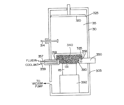
plasma, as illustrated in Fig. 3. A metal container 310 defines
the walls of a microwave cavity 315, the top of which can be a
plate 320, with finger stock 325, that serves as an adjustable
sliding short. An excitation probe 314 is provided, and its
position within the cavity can be made adjustable. A quartz
chamber or bell jar 335, which is used to contain a plasma 340,
is is mounted on a ring-shaped base 350 to which a vacuum chamber
305 and the microwave cavity 310 are attached. A gas injector
357 is used to feed a hydrocarbon and hydrogen mix into the
plasma forming region through apertures indicated at 358. A
cooling line 359 can be used to circulate a coolant to cool the
base, or cooling coils (not shown) can be provided. The insert
115, with substrate 131 thereon, is positioned on a support 392,
and a disc-shaped metal grid 380, can be used to define part of
the bottom of the microwave cavity, as shown. In operation, as
the mixture of hydrogen and hydrocarbon is fed in, microwave
energy in the cavity 315 creates the plasma 340, and
polycrystalline diamond will be deposited on the surface of
substrate 131. In a microwave plasma apparatus it is generally
beneficial to heat the substrate, and this may be implemented by
any suitable means, for example, with a susceptor plate. Also,
if desired, an apertured BN plate and/or cover can be used on the
insert (or on the entire holder) to protect edges from
overheating in the microwave field. A plasma jet deposition
apparatus could alternatively be used for deposition of the
diamond film, as could any other suitable deposition technique.
8
6 ,.
i


2~863f'~
DF-2244
A diamond film has a number of advantages for use as a
thermode tip. In addition to the recognized advantageous
properties of the diamond substance [including its thermal
conductivity, rigidity, long life, and resistance to wetting],
the diamond film can be deposited on surfaces having
predetermined shapes to avoid the necessity of machining diamond
to obtain different thermode tip configurations as in the case of
natural diamond. Deposition of the diamond film on a
polycrystalline diamond substrate, such as a sintered diamond
substrate, is particularly advantageous. A diamond substrate
facilitates the deposition growth of a diamond film of desirable
quality. Further, the diamond film surface prevents substances
such as cobalt or other metals or impurities in the underlying
substrate from contaminating parts being bonded or causing
undesired sticking. Also, the relatively close matching of the
coefficient of expansion of the diamond film to that of the
diamond substrate enhances the temperature performance and
longevity of the bonding tool. If desired, the deposited diamond
film can be polished, such as by lapping.
Alternative substrate materials having high elastic modulus
and good thermal conductivity can be utilized in conjunction with
a diamond film tip. For example, the substrate 131 and/or insert
115 or portions thereof could be cemented-tungsten carbide
(preferably, with a coating such as tungsten to separate the
diamond from the cementing agent), tungsten, silicon carbide, or
cubic boron nitride.
In accordance with a further form of the invention, a
ceramic substrate is provided which has a favorable thermal
conductivity property as well as substantial electrical
conductivity sufficient to permit shaping by electrical discharge
machining ("EDM"). Preferably, the substrate has thermal
conductivity of at least 60 W(m~°K)-~ and an electrical
resistance of less than 1000 ohm-cm. [The resistance encountered
9


2086367
DF-2244
by the EDM equipment also depends on geometry of the workpiece,
the value set forth being a general limit for typical
geometries.] A suitable ceramic which exceeds these requirements
is silicon carbide sintered with titanium diboride, which is sold
by Carborundum Company as*"Hexaloy ST". This material has good
thermal conductivity and electrical resistivity in the range 0.1
to 10 ohm-cm at room temperature. The electrical property makes
it machineable by EDM. The shaping of the hard materials used
for thermode substrates and/or tips is generally problematic, and
it is advantageous to use a ceramic which can be shaped by EDM
while still providing the thermal conductivity and rigidity
necessary for a thermode substrate and/or tip. After shaping,
the ceramic itself can be used as a tip, such as by employing it
as insert 115 (Fig.s 1, 2) or part thereof or attaching it to an
insert, or a tip can be applied, such as a tip of polycrystalline
diamond film as described above. Other electrically conductive
ceramic materials which are suitable for use in the described
manner are aluminum nitride doped with at least one dopant
selected from yttrium oxide, calcium oxide, dysprosium oxide, and
ytterbium oxide, and silicon carbide doped with at least one
dopant selected from beryllium and beryllium oxide.
The invention has been described with reference to
particular preferred embodiments, but variations within the
spirit and scope of the invention will occur to those skilled in
the art. For example, it will be understood that other tool
and/or holder configurations and other heating means could be employed.
*Trade-mark

Representative Drawing
A single figure which represents the drawing illustrating the invention.
Administrative Status

For a clearer understanding of the status of the application/patent presented on this page, the site Disclaimer , as well as the definitions for Patent , Administrative Status , Maintenance Fee  and Payment History  should be consulted.

Administrative Status

Title Date
Forecasted Issue Date 2000-02-22
(22) Filed 1992-12-29
(41) Open to Public Inspection 1993-07-11
Examination Requested 1994-02-01
(45) Issued 2000-02-22
Deemed Expired 2002-12-30

Abandonment History

There is no abandonment history.

Payment History

Fee Type Anniversary Year Due Date Amount Paid Paid Date
Application Fee $0.00 1992-12-29
Registration of a document - section 124 $0.00 1993-06-29
Maintenance Fee - Application - New Act 2 1994-12-29 $100.00 1994-11-15
Maintenance Fee - Application - New Act 3 1995-12-29 $100.00 1995-11-14
Maintenance Fee - Application - New Act 4 1996-12-30 $100.00 1996-12-20
Maintenance Fee - Application - New Act 5 1997-12-29 $150.00 1997-12-12
Maintenance Fee - Application - New Act 6 1998-12-29 $150.00 1998-12-16
Final Fee $300.00 1999-10-20
Maintenance Fee - Application - New Act 7 1999-12-29 $150.00 1999-12-03
Maintenance Fee - Patent - New Act 8 2000-12-29 $150.00 2000-12-01
Owners on Record

Note: Records showing the ownership history in alphabetical order.

Current Owners on Record
NORTON COMPANY
Past Owners on Record
HOGGINS, JAMES T.
HORTON, RALPH M.
KUO, SHIH-YEE
Past Owners that do not appear in the "Owners on Record" listing will appear in other documentation within the application.
Documents

To view selected files, please enter reCAPTCHA code :


To view images, click a link in the Document Description column. To download the documents, select one or more checkboxes in the first column and then click the "Download Selected in PDF format (Zip Archive)" or the "Download Selected as Single PDF" button.

List of published and non-published patent-specific documents on the CPD .

If you have any difficulty accessing content, you can call the Client Service Centre at 1-866-997-1936 or send them an e-mail at CIPO Client Service Centre.


Document
Description 
Date
(yyyy-mm-dd) 
Number of pages   Size of Image (KB) 
Description 1994-02-26 10 444
Cover Page 1994-02-26 1 20
Abstract 1994-02-26 1 35
Claims 1994-02-26 8 287
Drawings 1994-02-26 3 38
Description 1999-09-02 10 435
Claims 1999-09-02 8 306
Cover Page 2000-01-26 1 41
Representative Drawing 1998-10-29 1 6
Representative Drawing 2000-01-26 1 11
Correspondence 1999-10-20 1 26
Prosecution Correspondence 1994-02-01 1 30
Prosecution Correspondence 1998-11-02 2 81
Examiner Requisition 1998-07-31 2 81
Prosecution Correspondence 1997-08-18 2 85
Examiner Requisition 1997-02-18 3 127
Prosecution Correspondence 1994-04-22 1 24
Office Letter 1994-03-01 1 72
Fees 1996-12-20 1 55
Fees 1995-11-14 1 99
Fees 1994-11-15 1 78