Note: Descriptions are shown in the official language in which they were submitted.
P10280
-- 1 --
2086395
BACKGROUND OF TH~ INV~NTION
1. Field of the Invention:
The pre~ent invention relates to a film
capacitor having relia~le and excellent moisture re-
sistance, whiCh is suita~le as an electronic component
used in electronic or electric appliances, and a method
for manufacturing the same.
2. Description of the Related Art:
A film capacitor iS required to have improved
moisture resistance to improve its performance as an
electronic component. Also, studies are directed to
make a film capacitor, as well as electronic components
in general smaller and lighter. Regarding the mois-
ture resiStance, a film Capacitor has conventionally
been rated under the condition of 40~C and 95% relative
humidity (RH). Recently, however, the moisture resist-
ance of a film capacitor is required to be rated under
more severe conditions, such as tho~e of 60~C and
95~ RH, or 85~C and 85% RH, or 121~C, 2 atmospheres and
100~ RH (a condition of a pressure cooker test).
Among various film capacitors, there is known
a metallized film capacitor which-is made by forming a
metallic layer on a surface of a dielectric base film
and then stacking the thus metallized film. Because a
metallized film capacitor has very thin metallic
layers as electrodes and can be made small, it has
found an increasing demand egpecially as an electronic
component for lndustrial machines used under medium or
high voltage. A metallized film capacitor, however,
generally has a pro~lem o~ poor moisture resistance and
P10280
-- 2
20863qS
is far from satisfactory under the above-mentioned
moisture conditions.
A metallized film capacitor includes a
wound-type capacitor such as shown in Figure 5, and a
stacked-type capacitor such as shown in Figure 6. ~ach
of the capacitors can be manufactured in the following
manner. First, a multilayer structure of either a
wound metallized film or stacked metallized films is
prepared. Then, a pair of outer electrodes 12 are
formed on two side faces of the multilayer structure
opposing to each other. For example outer electrodes
are formed by the use of a metal spraying method,
thereby obtaining a capacitor element. Finally, the
capacitor element is either placed in an appropriate
casing or covered otherwise, thereby yielding a
desired capacitor.
In the manufacture of a stacked-type capaci-
tor, the manufacturing procedure can be described more
specifically as follows. First, metallized films
having a rectangular shape are stacked to each other,
thereby giving a multilayer structure. Second, a pair
of outer electrodes are formed on two side faces of
the multilayer structure opposing to each other, so as
to cover the longer edges of the rectangular metallized
films. Then, the thus obtained multilayer structure
having a pair of outer electrodes is cleaved along the
faces normal to the longer edges of the rectangular
metallized films, thereby obtaining capacitor elements
of specific sizes. Finally, the facets generated by
the above-mentioned cleavage~ are generally covered by
resin layers, thereby yielding desired stacked-type
P10280
-- 3
2086395
capacitors.
To the inside of the above-mentioned metal-
lized film Capacitors aS shown in Figures 5, 6A and
6B, moisture penetrates easily through the outer elec-
trodes 12, because these outer electrodes 12 have
porous structures. The penetration of moisture also
occ~rs easily through the dielectric films 11. In the
stacked-type CapaCitor aS shown in Figures 6A and 6B,
each of facets 14, which is generated by the cleavage
during the above-mentioned manufacturing proce~s, is
covered by a resin layer 1~. The resin layer 13,
however, can not completely prevent the penetration Of
moisture. The moisture that reaches the inside of the
capacitor may be condensed, resulting in defects of the
capacitor such as a decrease in the electric capacity.
In order to minimize the above-mentioned
problem, the capacitor element of a metallized film
capacitor has been either placed in a sealed resin
casing or provided with a sufficiently thick resin
layer as the resin layer 13. The resin layer 13 may be
extended so as to cover the entire surface of the
capacitor element
Figure 7 is a conceptual view showing a
partial cross section of a stacked-type capacitor. The
capacitor element of the stacked-type capacltor in-
cludes a multilayer structure made of metallic layers
15-and dielectric films 16, and outer electrodes 17
electrically connected to the metallic layers 15. A
side face of the multilayer structure is covered by a
resin layer 13 whiGh i~ made of ~rethane resin or epoxy
P10280
-- 4
208~3q~
resin. In a conventional capacitor such as shown in
Figure 7, the resin layer 13 cannot completely prevent
the penetration of moisture Z1 from the outside of the
capacitor. Once penetrated into the inside of the
capacitor, moisture may be easlly condensed according
to the change in temperature thereby giving water
particle~ 22 and 23. These water particles 22 and 23
cauSe corrosion and elution of the metallic layers 15,
resulting in a decrease in the electric capacity. Fur-
thermore, the resin layer 13 which is in contact with
the metallic layers 15 tends to he partially removed to
give interspaces along the facet (i.e., cleaved sur-
face) of the multilayer structure. These interspaces
may collect the water particles 22 and 23, thereby
accelerating the corrosion of the metallic layers 15.
The facet of the multilayer structure is susceptible
to corrosion especially when voltage i~ applied to the
capacitor, because of the electrolytic reaction.
Regarding the size of the capacitor, a mi-
crominiature chip metallized film capacitor has been
recently developed, which has a contact area of
~.2 mm x 1.6 mm with regard to a substrate on whiCh the
capacitor iS to be mounted. In such a microminiature
Capacitor, a resin layer required to provide the capac-
itor with moisture resistance occupies a considerable
volume of the capacitor, thereby preventing the further
miniaturization of the capacitor.
Japanese Laid-Open ~atent ~ublication
No. 63-181409 discloses a method for coating a thin
re~in layer on the surface of a chip film capacitor
except for the surface of the outer electrode~ of the
-
P10280
-- 5
2086395
capacitor and for the surface of ~he capacitor which
is to be in contact with a printed circuit board.
Japanese Laid-Open Patent Publication No. 64-77911
discloses a method for forming resin layers on the two
facets generated by the cleavage of a chip film capaci-
tor. Japanese Laid-Open Patent Publication
Nos. 64-77913, 64-77917 and 64-77920 disclose methods
for fixing by heat and pressure a specific sheet
material as a coating layer on the surface of a capaci-
tor. Japanese Laid-Open Patent Publication No. 2-43718
discloses a method for applying and curing a resin
layer on the facet of a capacitor. According to these
methods, the volume of the coating layer of a chip film
capacitor can be made significantly small.
As a metallized film capacitor is further
miniaturized, precise operation becomes more difficult
for coating a resin sheet thereon or applying a resin
solution thereto. With regard to productivity, an
advantageous coating method would be, for example, a
method of immersing a number of capacitor elements at
the same time into a resin solution. This coating
method, however, cannot be employed for the manufacture
of a chip film capacitor, because the resin layer is
required to be formed only on specific faces including
the facets of the capacitor, without covering the outer
electrodes of the capacitor.
SUMMARY OF TEIE INVENTION
The film capacitor of thi~ invention
comprises: a capacit~r element having (a) a multilayer
stru~ture made o~ stacked dielectric resin f ilms or a
20863~5 P10280
-- 6
wound dielectric resin film, each dielectric film
having a metallic layer formed on its surface, and (b)
a pair of outer ele~trode~ electrically connected to
the metallic layer; and
a moisture pe~etrated, microporous coating layer
covering at least facets of the multilayer structure of
the capacitor element, the coating layer having a
cross-linked structure and being made from a coating
material consisting essentially of polysiloxane,
organometallic compound or a combination of the
polysiloxane and the organometallic compound, the
organometallic compound being selected from the group
consisting of organoaluminum compounds, organosilicon
compounds, organotin compounds and organotitanium
compounds; and wherein the organomethallic compound has
at least one functional group attached to the metallic
atom of the organometallic compound, the functional
group being reactive to inorganic or organic materials
and represented by the formula -OR, R being selected
from the group consisting of hydrogen, hydrocarbyl,
oxygen-containing hydrocarbyl, nitrogen-containing
hydrocarbyl and oxygen- and nitrogen-containing
hydrocarbyl.
The method for manufacturing a film capacitor
of this invention comprises the steps of: preparing a
capacitor element having (a) a multilayer structure
made of stacked dielectri~ resin films or a wound
dielectric resin film, each dielectric film having a
metallic layer formed on its surface, and (b) a pair of
outer electrodes electrically connected to the metallic
layer; and providing at least facets of the multilayer
structure with a moisture penetrated, microporous
coating material so as to form a coating layer having
cro~-linked structure and being made from a coating
material consisting es~entially of polysiloxane,
' ;~
2086395
P10280
-- 7
organometallic compound or a co~bination of the
polysiloxane and the organometallic compound, the
organometallic compound being selected from the group
consisting of organoaluminum compounds, organosilicon
compounds, organotin co~pounds and organotitanium
compounds; and wherein the o~ganometallic compound has
at least one fun~tional group attached to the metallic
atom of the organometallic compound, the functional
group being reactive to inorganic or organic materials
and represented by the formula -OR, R being ~ele~ted
from the group consisting of hydrogen, hydrocarbyl,
oxygen-containing hydrocarbyl, nitrogen-containing
hydrocarbyl and ~xygen- and nitrogen-containin~
hydrocarbyl.
~hu~, the invention described herein makes
possible the advantages of (1) providing a film capaci-
tor having excellent moisture resistance; (2) providing
a microminiature chip film capacitor having excellent
moisture resistance, which includes outer electrodes
having improved wettability for solder; and (3) pro-
viding a method for manufacturing the above capacitors
in a manner Convenient and suitable for mass produc-
tion.
These and other advantage~ of the present
invention will become apparent to those skilled in the
art upon reading and understanding the following de-
tailed description with reference to the accompanying
figures.
BRIEF DESCRIPT~N ~F ~HE DRAWINGS
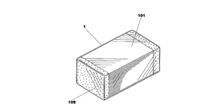
Figure 1 i~ a perspective view illustrating
an embodiment of the film capacitor according to the
2 0 8 6 3 9 5 Pl0280
pre~ent invention which is a chip film capacitor ob-
tained in ~xample 1.
Figure 2 is a schematic sectional view illus-
trating an embodiment of the film capacitor according
to the present invention.
Figure 3A is a partially cutaway perspective
view illustrating an embodiment of the film capacitor
according to the present invention.
Figure 3B is a sectional view, taken on
section lines A-B-C-D of Figure ~A.
Figure 4 is a schematic sectional view illus-
trating an embodiment of the film capacitor according
to the present invention.
Figure 5 is a partially cutaway perspective
view illustrating a conventional wound-type film
capacitor
Figure 6A is a partially cutaway perspective
view illustrating a conventional stacked-type film
capacitOr.
Figure 6B is a sectional view, taken on
section lines A'-B'-C'-D' of Figure 6A.
- 30 Figure 7 is a conceptual view illu~tratin~
corrosion Of metall1c layer~ of a conventional
stacked-type film capacitor.
P10280
_ g
2086395
Figure 8 is a graph illustrating the result
of a moisture resistance test, which was performed for
film capacitors obtained in ~xample 5 and Comparative
example 1.
Figure 9 is a schematic representation illus-
trating a step of providing a capacitor element with a
coating material according to an embodiment of the
manufacturing method of the present invention.
Figures 10, 11 and 12 are schematic represen-
tations illustrating a step of providing a capacitor
element with a coating material, which includes a
immersing step, according to an embodiment of the
manufacturing method of the present invention.
Figure 13 is a graph illustrating the result
of a moisture resistance test, which was performed for
film capacitors obtained in ~xample 1 and Comparative
examples 4 and 5.
Figure 14 is a graph illustrating the result
of a soldering wettability test, which was performed by
using solder meniscograph for film capacitors obtained
in Example 1 and Comparative exampIes 4 and 5.
Figure 15 is a graph illustrating the result
of a reflow soldering test, which was performed for
film capacitors obtained in Examples 1, 25, 26 and 27.
Figure 16 is a graph ill~strating the result
Of a soldering wettability test, which was performed ~y
using f~r film capacitors obtalned in ~xample~ 1, 25,
P10280
-- 10 --
20863q5
26 and 27.
DE;SCRIPTION OF THE PREFERRED EMBODIMENTS
In the film capacitor of this invention,
resin films such as those generally used for a film
capacitor is used as a dielectric base film for a
metallized film. Examples of the suitable resin films
include polyester resin film, polypropylene resin film,
polyphenylene resin film and laminate films made of a
combination thereof. Although this invention is not
limited regarding the material of the dielectric base
film, polyester resin film is preferably used. Fur-
ther, this invention is not limited regarding the
thickness of the dielectric base film. However, the
thickness of the dielectric base film is normally
0.1 - 30 ~m, and preferably 0. 6 - 15 ~m.
In this invention, a metallized film means a
film prepared by forming a metallic layer on at least
one side of the above-mentioned dielectric base film.
The material of the metallic layer can be aluminum or
zinc which are generally used as electrodes of a film
capacitor. Neither the method for forming the metallic
layer nor the thickness of the metallic layer is
limited. Available method~ for forming the metallic
layer include vacuum evaporation, sputtering and ion-
plating. Thickness of the metallic layer is normally
200 - 1000 A, and preferably 250 - 700 A.
The coating material used for the film capac-
itor of this invention i~ divided into two classes.
~he fir~t class iS polysiloxane represented generally
P10280
-- 11 --
2086395
by Formula I.
R3 - (Si ~ ~)n 4
R2
(Formula I)
In Formula I, R1, R2, R3 and R4 are independ-
ently hydrogen, alkyl, phenyl, hydroxyl, oxygen-con-
taining hydrocarbyl, nitrogen-containing hydrocarbyl,
oxygen- and nitrogen-containing hydrocarbyl or siloxa-
nyl (su~stituent derived from silicone), and n is an
integer of 2 or more. More specifically, R1, R2, R3
and R4 include vinyl, alkoxy, acyloxy such as acetoxy,
epoxyl, amino, acryloyl, methacryloyl, epoxy such as
glycidoxyalkyl, silanol, isocyanate, an organic moiety
containing a hydroxy group and an organic moiety con-
taining a carboxy group.
Polysiloxane of Formula I includes methylhy-
drogenpolysiloxane, dimethylpolysiloxane and the like.
The polysiloxane itself can polymerize to form a ~ili-
cone resin having a cross-linked network structure.
Furthermore, the polysiloxane can polymerize with an
another reactive resin to form a copolymer (i.e. a
denatured silicone resin). The reactive resin includes
alkyd resinr polyester resin, epoxy resin, amide resln,
imide resin, fluoride-contalned re~in, urethane resin
and acrylic resin
P10280
- 12 - 2086395
The second cla~ is an organometallic com-
pound which has at least one functional group attached
to the metallic atom of the organometallic compound.
This functional group is represented by the formula
-OR, where R is hydrogen, hydrocarbyl, nitrogen-
containing hydrocarbyl, oxygen-containing hydrocarbyl
and oxygen- and nitrogen-containing hydrocarbyl. The
above organometallic compound includes organoaluminum
compounds, organosilicon compounds, organotin compounds
and organotitanium compounds, and is represented gener-
ally by Formula II.
(R ) M (OR )
5 n-m 6 m
(Formula II)
In Formula II, M is a metallic atom which is
aluminum, silicon, tin or titanium, m is an integer of
1, 2, 3 or 4 with the proviso of m S n; n is 3 when M
is aluminum, or 4 when M is silicon, tin or titanium;
and R5 and R6 are independently hydrogen, hydrocarbyl,
oxygen-containing hydrocarbyl, nitrogen containing
hydrocarbyl and oxygen- and nitrogen-containing hydro-
carbyl. More specifically, R5 and R6 include vinyl,
alkoxy, acyloxy such as acetoxy, epoxyl, amino, acryl-
oyl, methacryloyl, expoxy such as glycidoxyalkyl, sila-
nol, isocyanate, an organic moiety containing a hydroxy
group, an organic moiety containing a carboxy group
The organoaluminum compounds Of Formula II
include aluminum trietho~ide, aluminum triisopropo~ide,
derivatives thereof, and polymers thereof. The organo-
silicon compounds of Formula I I include dimethyldime-
P10280
- 13 - 208 63q 5
thoxysilane, vinyltrimethoxysilane, methyltriethoxysi-
lane, hexyltrimethoxysilane, methyltrimethoxysilane,
tetramethoxysilane, tetraethoxysilane, methylhydrogen-
dimethoxysilane, dimethylvinylethoxysilane, diphenyl-
dimethoxysilane, gamma-(2-aminoethyl)aminopropyltrime-
thoxysilane, gamma-(2-aminoethyl)aminopropylmethyldime-
thoxysilane, gamma-methacryloxypropyltrimethoxysilane,
gamma-glycidoxypropyltrimethoxysilane, gamma-
mercaptopropyltrimethoxysilane, vinyltriacetoxysilane,
gamma-anilinopropyltrimethoxysilane, derivative~ there-
of, and polymers thereof. The organotin compounds of
Formula II include tin tetra-n-butoxide, derivatives
thereof, and polymers thereof. The organotitanium com-
pounds of Formula II include titanium tetraisopropox-
ide, titanium tetra-n-butoxide, titanium tetrakis(2-
ethylhexoxide), titanium diisopropoxide bis(acetyla-
cetonate), titaniUm di-n-butoxide bis(triethanolami-
nate), derivatives thereof, and polymers thereof.
The coating material used for the film capac-
itor of this invention may contain an additional com-
pound whiCh Can be cured by UV irradiation, thereby
yeilding a coating material which as a whole can be
cured by UV irradiation. A coating layer having de-
sired hardness can be obtained from a coating material
containing an appropriate compound.
The film capacitor of this invention can be
manufactured in the following manner. First, a metal-
lic layer is formed at least on one side of the above-
mentioned dielectric base film, thereby yielding a
metallized film. Second, the metallized film is stacked
by the conventional method into a multilayer structure.
P10280
- 14 -
20863q~
~ext, A pair of outer electrode 12 were formed on two
side faces of the multilayer ~tructure opposing to each
other, so as tO cover the longer edges of the metal-
lized films, by a metal spraying method. Then, the
thus obtained multilayer structure having a pair Of
outer electrodes was cleaved along the faces normal to
the longer edges of the rectangular metallized films,
thereby yielding a capacitor element 101 as shown in
Figure 9. This capacitor element 101 is then immersed
into a solution 102 containing the above-mentioned
coating material such as organosilicon compound, or
the other organometalli~ compound Appropriate sol-
vent for dissolving the coating material includes an
inert solvent such as n-heptane, toluene, xylene or
trichlorofluoroethane, and an organometallic compound
such as methyltrimethoxysilane. The abo~e immersing
step may be effectively carried out, as shown in Figure
10, by placing a number of the capacitor elements 101
in a Cage 107, and then immersing the cage 107 into the
solution 102. An ultrasonic vibrator 103 may be used
during the immersing step so as to facilitate contact
between the entire surfaces of the capacitor elements
101 and the solution 102. In this ultrasonic treat-
ment, the solution 102 may penetrate even into a part
Of the multilayer structure of the capacitor element
101. The solution 102 has preferably a viscosity at
25~C of not more than 3.2 x 10 Pa-s preferably, not
more than 2 x 10 Pa-s (0 02 poise), so as to assure
formation on the surface of the capaCitor element 101
of an extremely thin coating layer SUCh as a monomolec-
ular layer. The immersing step is followed, as shown
in Figure 11, by a ~tep ~f withdrawing the cage 107
from the solution 102 so as to remo~e excessi~e coating
P10280
- 15 - 2086395
material. Then, the capacitor element 101 having the
coating solution on its surface may be heat-treated, as
shown in Figure 12, at 100~C - 200~C, for example, in
an air circulating-type thermostat controlled oven 109
80 a~ to cure the coating material into a coating
layer. When the coating material includes the organo-
metallic compound, this heat-treatment allows formation
of a chemical bond between the metallic atom of the
organometallic compound and the surface of the capaci-
tor element 101. When the coating material includes
the polysiloxane having a reactive functional group,
the heat-treatment results in the same type of chemical
bond formation. In addition, when the organometallic
compound or the polysiloxane has a hydrophobic group,
this chemical bond formation places the hydrophobic
group within the coating layer on the opposite side
from the surface of the capacitor element 101. The
above heat-treatment also allows evaporation of any
excessive coating material which may slightly remain in
an interspace between the two capacitor elements be-
cause of surface tension. In thiS way, the Coating
layer iS formed on the entire surface of each of the
capacitor elements 101 which includes the surface of
the outer electrodes 12. The coating layer may be also
formed on a surface of the cage 107. Because these
coating layers are substantially monomolecular layers
which are extremely thin, the cUring process in the
heat-treatment does not cause adhesion between the
capacitor element 101 and the cage 107, or adhesion
amor~g each of the capacito~ element~: ~hu~, the coated
capacitor element~ can be ea~lly recovered from the
cage 107
P10280
- 16 -
2086395
The manufacturing method of this invention is
suitable for mass-production of the film capacitor,
because the manufacturing method may include a step,
Such as the above-mentioned immersing step, in which a
number of capacitor elements can be coated at once.
In addition, the manufacturing method of this
invention enables formation of an extremely thin coat-
ing layer on a film Capacitor element, which may be
several microns in the thickness. ~he thickness of the
coating layer can be controlled, for example, by chang-
ing the concentration of the solution containing the
coating material. Such an extremely thin coating layer
would greatly facilitate miniaturization of the capaci-
tor, because the coating layer can occupy a minimal, oreven negligible volume of the capacitor.
As mentioned above, the manufacturing method
of this invention uses coating material including the
polysiloxane or the organometallic compound. The use
of these specific coating materials results in close
contact between the resulting coating layer and the
surface of a capacitor element For example, the
organometallic compound can be chemically bound to the
surface of the Capacitor element, which includes sur-
faces of the metallic layer, the dielectric film and
the outer electrodes of the capacitor element. Also,
the polysiloxane has a high degree of affinity to the
surface of the capacitor element This affinity is
especially high when the dielectric film of the capaci-
tor element is made of a polyester resin film, such as
polyethylene naphthalate or polyethylene terephthalate.
P10280
- 17 -
20863q5
The above organometallic compound can form a
polymer having a cross-linked structure, resulting in a
m~croporous coating layer on the ~urface of the capaci-
tor element. Through thiS microporous coating layer,
moisture penetrateS easily. The above polysiloxane,
especially silicone resin and denatured silicone resin,
may have cross-linked Si-0 bonds within the polymer
molecule. Thus, the poly~iloxane can also form a
mi~roporou~ coating layer, miCroporeS of WhiCh have
larger diameters than a water molecule. The micropor-
oUs coating layers formed in the above manners are
advantageous in that even if moisture has once reached
the inside of the capacitor element, it i~ readily re-
leased to the outside. The coating layer may be highly
hydrophobic, for example, when it is made of the
polysiloxane having cross-linked Si-0 bonds. In addi-
tion, as mentioned above, the coating layer of the film
capacitor of this invention is placed in close contact
to the surface of the capacitor element. Therefore,
the film capacitor of this invention hardly suffers
from adverse effects of penetration and condensation
of moisture, such as deterioration of its performance.
Example 1
Figure 1 illu~trate~ an embodiment of the
film capacitor according to the present invention.
An aluminum layer having a thickness of
approximately 500 A was formed on a polyphenylene
sulflde film having a thickness of approximately 2.0 ~m
by vacuum evaporation, thereby giving a metallized
polyphenylene sulfide film. This metallized ~ilm was
stac~ed into a mult~layer ~trUGture~ ~ p~ir o~ oute~
P10280
- 18 -
20863~5
electrode 105 were formed on two side faces Of the
multilayer structure opposing to each other, so as to
cover the longer edges of the metallized films, by a
metal spraying method. Then, the thus obtained multi-
layer structure having a pair of outer electrodes was
cleaved along the faces normal to the longer edges of
the re~tangular metallized films, thereby giving a film
capaCitor element 101. AS shown in Figure 10, a number
Of the capacitor elements lO1 obtained in this manner
were placed in a cage 107, which was then placed in a
bath 106 ha~ing a solution 102 ~ontaining methyltrime-
thoxy~ilane, thereby immersing the capacitor elements
101 into the solution 102. The concentration of meth-
yltrimethoxysilane in the solution 102 had been adjust-
ed so that the solution 102 had a viscosity at 25~C of
about 0.7 x 10 Pa-s. During the immersing ~tep, the
solution 102 wa~ vibrated from the outside by the use
of an ultrasonic vibrator 103 so as to facilitate
contact between the entire surfaces of the capacitor
elements 101 and the solution 102. After the immersing
step, as shown in Figure 11, the cage 107 was withdrawn
from the solution 102, thereby removing ea~ily an
exces~ amount of the solution of methyltrimethoxysi-
lane. Then, aS shown in Figure 12, the cage 107 having
the capacitor elements 101 was transferred into an air
circulating-type thermostat controlled oven 109 heated
at a temperature between 100~C and 200~C, thereby
curing the methyltrimethoxysilane adhering to the
entire surfaces of the capaCitor elements 101. ThiS
heating step also allowed evaporation of any e~ce~
amount of methyltrimetho~ysilane Which h~d remained
~lightly in inte~p~es between the capacitor element~
101 because of surface ten~ion ~he methyltrlmethox-
P10280
_ 19 --
~086395
ysilane adhering to the entire surfaces of the capaci-
tor elements 101, which include the surfaces of the
outer electrodes 105, formed extremely thin layer~ 1 as
shown in Figure 1. Therefore, the curing process in
the heating step did not cause undesirable adhesion
among each of the capacitor elements 101.
Example 2
Figure 2 illustrates another embodiment of
the film capacitor according to the present invention.
A metallized film having a thickness of
approximately 2.0 ~m was prepared by evaporating an
aluminum layer on a polyethylene naphthalate (PEN)
film. This metallized film was stacked into a multi-
layer structure, a pair of outer electrodes were formed
on two side faces of t~e multilayer structure opposing
to each other, so as to cover the longer edges of the
metallized film~, by a metal spraying method. Then,
the thu~ obtained multilayer structure having a pair of
outer electrodes was cleaved along the faces normal to
the longer edges of the rectangular metallized films.
Then, a lead 55 was attached to each of the outer
electrodes 51, thereby giving a film capacitor element
52. This capacitor element 52 was then immersed into
a solution containing methylhydrogenpolysiloxane. The
immersing step was followed by a heat-treatment at
150~C for l hour, thereby forming a coating layer 53
made of silicone resin on the surface of the capacitor
element This coatqd capacitor element wa~ further
covered by an epoxy re~in layer 54 having a thic~ness
of 0.5 mm.
P10280
- 20 -
20863q5
~xample 3
Figures 3A and 3B illustrate still another
embodiment of the f ilm capacitor according to the
present inventlon.
A metallized film having a thickness of
approximately ~.5 ~m was prepared by evaporating an
aluminum layer 62 on a polyethylene naphthalate (P~N)
film 61. This metallized film was stacked into a
multilayer structure, a pair of outer electrodes 63
were formed on two side faces of the multilayer struc-
ture opposing to each other, so as to cover the longer
edges of the metallized ~ilms, by a metal spraying
method. Then, the thus obtained multilayer structure
having a pair of outer electrodes was cleaved along the
faces normal to the longer edges of the rectangular
metallized films, thereby giving a film capacitor
element 64 of a surface mount-type. This capacitor
element 64 was subjected to a heat aging at a tempera-
ture of 220~C or more, so that the capacitor element 64
was applicable to a reflow soldering operation. Then,
a solution containing methylhydrogenpolysiloxane was
applied to exposed facets 66 of the capacitor element
64, which were also cleaved surfaces of the multilayer
structure. By heat-treating the capacitor element 64
at 150~C for 1 hour, coating layers 65 made of sili-
cone resin were formed on the facets 66. These coated
facets 66 were further covered by epoxy resin layers 67
each having a thickness of 0.05 mm.
Example 4
The pLoced~re o~ Example ~ was followed
except that resin layers were not formed on the coated
P10280
- 21 -
2086395
facets.
Example 5
~he pro~edure of Example 2 was followed
except that addition-polymerizable silicone was used as
a coating material instead of methylhydrogenpolysilox-
ane. This film capacitor had a coating layer made of
cross-linked dimethylpolysiloxane having a thickness of
approximately 0.05 mm, and a re~in layer having a
thickne~s of approximately 0.5 mm.
~xample 6
The procedure of Example 3 was followed
except that addition-polymerizable-~ilicone was u~ed a~
a coating material instead of methylhydrogenpolysilox-
ane. A coating layer made of cross-linked dimethylpo-
lysiloxane of this film capacitor had a thickness of
approximately 0.05 mm.
Example 7
The procedure of Example 4 was followed
except that dimethylpolysiloxane was used as a coating
material instead of methylhydrogenpolysiloxane.
Example 8
Still another embodiment of the film capaci-
tor according to the present invention was o~tained in
the following manner.
A metalllzed film having a thlckne~: of
approxlmately ~ 5 ~m wa~ prepared by evaporatin~ an
aluminu~ layer on a p~lyethylene napnthalate ( P~N)
film. ThiS metallized film was stac~ed into a multi-
P10280
- 22 - 208 63q 5
layer structure, a pair of outer electrodes were formed
on two side faces of the multilayer structure opposing
to each other, So as to cover the longer edges of the
metallized films, by a metal spraying method. Then,
the thus obtained multilayer structure having a pair of
outer electrodes wa~ cleaved along the faces normal to
the longer edges of the rectangular metallized films,
thereby giving a film capacitor element of surface
mount-type. This capacitor element was then immersed
into a n-heptane solution containing 5 wt~ of
addition-polymerizable-silicone. After being air-
dried at room temperature for 30 min, the immersed
capacitor element waS heat-treated at 150~C for 1 hour,
thereby forming a coating layer made of cross-linked
dimethylpolysiloxane on the surface of the capacitor
element. The coating layer had a thickness of approxi-
mately 2 ~m
~xample 9
Figure 4 illustrates still another embodiment
of the film capacitor according to the present inven-
tion.
A metallized film having a thickness of
approximately 2.0 ~m was prepared by evaporating an
aluminum layer on a polyethylene naphthalate (PEN)
film. This metallized film was stacked into a multi-
layer structure, a pair of outer electrodes were formed
on two side faces of the multilayer Structure opposing
to each other, so as tO cover the longer edges ~ the
metallized films, ~y a metal spraying method. Then,
the thus ~btained multilayer structure having a pair of
~ter electrode~ waq clea~ed along the faces normal to
P10280
- 23 -
~0863q5
the lon~er edges of the rectangular metallized films.
Then, a lead was attached to each of the outer elec-
trodes, thereby giving a film capacitor element 71. An
addition-polymerizable silicone was applied to expo~ed
facets 72 of the capacitor element 71, which were also
cleaved surfaces of the multilayer structure. By
heat-treating the capacitor element 71 at 150~C for
1 hour, coating layers 73 made of a denatured silicone
obtained by the reaction of an addition-polymeriza~le
silicone with a epoxy group were formed on the facets
72. The~e coated facets 72 were further covered by
epoxy resin layers 74 having a thickness of 0.05 mm.
Then, the thus obtained film capacitor was inserted in
the box 75 of polycarbonate resign.
Example 10
The procedure of Example 2 was followed
except that hexyltrimethoxysilane was used as a coating
material instead of methylhydrogenpolysiloxane.
Example 11
The procedure of Example 3 was followed
except that metyltriethoxysilane was used as a coating
material instead of methylhydrogenpolysiloxane.
Example 12
The procedure of Example 4 was followed
except that metyltriethoxysilane was used as a coatin~
material instead of methylhydrogenpolysiloxane.
Example 13
The procedure of Example 2 was followed
except that titanium diisopropoxide bis(acetylaceto-
P10280
- 24 -
20863~
nate) was used as a coating material instead of met-
hylhydrogenpolysiloxane.
Example 14
The procedure of ~xample 3 was followed
except that titanium diisopropoxide bis(acetylaceto-
nate) was used as a coating material instead of met-
hylhydrogenpolysiloxane.
Example 15
The procedure of ~xample 4 was followed
except that titanium diisopropoxide bis(acetylaceto-
nate) was used as a coating material instead of met-
hylhydrogenpolysiloxane.
Example 16
The procedure of ~xample 2 was followed
except that a polymer o~ titanium tetra-n-butoxide was
used as a coating material instead of methylhydrogenpo-
lysiloxane
~xample 17
The procedure of Example 3 was followed
except that a polymer of titanium tetra-n-butoxide was
used as a coating material instead of methylhydrogenpo-
lysiloxane.
~xample 18
The procedure of Example 4 was followed
except that a polymer of titanium tetra-n-butoxide was
used as a coating material instead of methylhydrogenpo-
lysiloxane.
Pl0280
- 25 -
2086395
Example 19
The procedure of ~xample 2 was followed
except that aluminum triisopropoxide was used as a
coating material instead of methylhydrogenpolysiloxane.
Example 20
The procedure of Example 3 was followed
except that aluminum triisopropoxide was used as a
coating material instead of methylhydrogenpolysiloxane.
Example 21
The procedure of Example 4 was followed
except that aluminum triisopropoxide was used as a
coating material instead of methylhydrogenpolysiloxane.
Example 22
The procedure of Example 2 was followed
except that tin tetra-n-butoxide was used as a coat-
ing material instead of methylhydrogenpolysiloxane.
Example 23
The procedure of Example ~ was followed
except that tin tetra-n-butoxide was used as a
coating material instead of methylhydrogenpolysiloxane.
Example 24
The procedure of Example 4 was followed
except that tin tetra-n-butoxide was used as a coat-
ing material instead of methylhydrogenpolysiloxane.
3~
Comparati~e ~xample 1
A metallized film ha~ing a thickness Of
approximately 2 0 ~m was prepared by evaporating an
P10280
- 26 -
3 ~ ~
aluminum layer on a polyethylene naphthalate (PEN)
film. This metallized film was stacked into a multilay-
er structure, a pair of outer electrode were formed on
two side faces of the multilayer structure opposing to
each other, so as to cover the longer edges of the
metallized films, by a metal spraying method. Then,
the thus obtained multilayer structure having a pair of
outer electrodes was cleaved along the faces normal to
the longer edges of the rectangular metallized films.
Then, a lead wa~ attached to each of the outer elec-
trodes, thereby giving a film capacitor element. The
entire surface of this capacitor element was covered
by an epoxy resin layer having a thickness of O.S mm.
Comparative Example 2
A metallized film having a thickness of
approximately 3.5 ,um was prepared by evaporating an
aluminum layer on a polyethylene naphthalate ( PEN )
film. This metallized film was stacked into a multilay-
er structure, a pair of outer electrode were formed on
two side faces of the multilayer structure opposing to
each other, So as to cover the longer edges of the
metallized films, by a metal spraying method. Then,
the thus obtained multilayer structure having a pair of
outer electrodes was cleaved along the faces normal to
the longer edges of the rectangular metallized films,
thereby giving a film capaCitor element of a surface
mount-type. This capacitor element was subjected to
heat aging at a temperature of 220~C or more, so that
the capacitor element was applicable to a reflow sol-
derlng operatlon. ~he entlre surface of thls capacl-
tor element was covered by an epoxy resin layer having
a thickness of 0.05 mm.
P10280
- 27 -
20863q5
Comparative Example 3
The procedure of Comparative ~xample 2 was
followed except that a resin layer was not formed on
the capacitor element, which itself was used as a film
capacitor.
Test 1
A moisture resistance test was performed for
the film capacitors of Examples 2 through 24, and for
those of Comparative Examples l through 3. In this
test, DC voltage of lO0 V was applied to each film
capacitor under the conditions of 85~C and 85~ RH, and
variation per hour of the electric capacity of each
film capacitor was followed. For each of the Examples
and Comparative Examples, the result was obtained from
the average electric capacity of 12 samples.
Figure 8 Compares the result obtained for the
film capacitor of ~xample 5, which has a coating layer
of cross-linked dimethylpolysiloxane and an epoxy resin
layer, and that of Comparative Example l, which has
only an epoxy resin layer.
Tables l, 2 and 3 show the average time for
each film capacitor for the variation rate to reach -5
(Hours).
P10280
- 28 -
20~6~
Table l
The average time for the varia-
tion rate to reach -5~ (Hours)
Example 2 1500
Example 5 ~ 2000
Example 9 ~ 2000
Example 10 1750
Example 13 1500
Example 16 1500
~xample 19 1250
~xample 22 1250
Comparative
Example 1 600
Table 2
The average time for the varia-
tion rate to reach -5~ (Hours)
Example 3 1250
~xample 6 ~ 2000
~xample 11 1500
Example 14 1500
Example 17 1250
Example 20 1000
Example 23 1000
Comparati~e
Example 2 500
P10280
- 29 -
2086395
Table 3
The average time for the varia-
tion rate to reach -5~ (Hours)
~xample 4 1000
Example 7 800
Example 8 1750
Example 12 lO00
Example 15 900
Example 18 800
Example 21 700
~xample 24 700
Comparative
~xample 3 300
As seen from the results shown in Figure 8
and Tables 1, 2 and 3, formation of a coating layer of
polysiloxane or organometallic compound greatly im-
proves the moisture resistance of a film capacitor.
Comparative Example 4
An aluminum layer having a thickness of
approximately 500 A was formed on a polyphenylene
sulfide film by vacuum evaporation, thereby giving a
metallized polyphenylene ~ulfide film. This metal-
lized film waS stacked into a multilayer structure, a
pair of outer electrode were formed on two side faces
of the multilayer structure opposing to each other, so
as to co~er the longer edges of the metallized film~,
by a metal spraylng method Then, the thus obtained
multilayer ~tru~ture having a pair of outer electrode~
was cleave~ alon~ the faces normal to the lonqer e~ges
P10280
- 30 -
20&63q~
of the rectangular metallized films, thereby giving a
film capacitor element. On exposed facets of this
capacitor element, which were also cleaved surfaces of
the multilayer structure, coating layers made of a UV-
curing resin were formed according to the method dis-
closed in Japanese Laid-Open Patent Publication
No. 2-43718.
Comparative Example S
The procedure of Comparative Example 4 was
followed except that a resin layer was not formed on
the capacitor element, which itself was used as a film
capacitor.
Test 2
A Moisture resistance test was performed for
the film capacitors of Example 1 and Comparative Exam-
ples 4 and 5. In this test, a DC voltage of 16 V was
applied to each film capacitor under the conditions of
60~C and 95% RH, and variation per hour of the electric
capacity of each film capacitor was followed.
Figure 13 shows the results obtained for
these film capacitors. As seen from Figure 13, the film
capacitor of Example 1, which has a coating layer made
from methyltrimethoxysilane, has greatly improved
moisture resistance as compared with the film capaci-
tors of Comparative Examples 4 and 5.
Then, a soldering test was performed for the
film capacitors of Example 1 and comparative Examples 4
and 5. In this test, each fllm capacitor was subjected
to reflow soldering by solder paste within a hot-air
Pl0280
- 31 -
2086395
reflow furnace at the maximum temperature of 230~C.
For each of Example l and Comparative Examples 4 and
5, 5000 sample~ were soldered.
Table 4 shows the result of the soldering
test. As seen from Table 4, no soldering failure was
found for any of the film capacitors.
Table 4
The rate of soldering failure
Example l 0
Comparative
Example 4 0
Comparative
~xample 5 0~
Further, a soldering wettability test was
performed for the film capacitors of Example l and
Comparative Examples 4 and 5. In this test, each film
capacitor was placed in a solder bath heated at 230~C,
and the time required for the film capacitor tO become
free from stress given by melted solder was measured
by the use of meniscograph. For each of Example l and
Comparative Examples 4 and 5, 50 samples were tested.
Figure 14 shows the result of the soldering
wettability test. As seen from Figure 14, all of the
film Capacitors showed excellent soldering wettability.
Example 25
The procedure of Example l wa~ followed
except that 5 wt~ of an addition-polymeriza~le silicone
P10280
- 32 -
208639~
was added to the solution containing methyltrimethox-
ysilane. This addition-polymerizable silicone ~an
form cross-linked dimethylpolysiloxane by heat-treat-
ment. The solution used in this Example had a visco~ity
at 25~C of ~.2 x 10 Pa~s as measured by a coneplate-
type vi~cometer.
~xample 26
The procedure of Example 25 was followed
except that ~ wt~ of the addition-polymerizable sili-
cone wa~ added to the ~olution containing methyl-
trimethoxysilane. The solution used in thiS ~xample
had a viscosity at 25~C of 2.2 x 10 Pa-s as measured
by a coneplate-type viscometer.
Example 27
The procedure of Example 25 was followed
except that 1 wt~ of the addition-polymerizable sili-
cone was added to the solution containing methyl-
trimethoxysilane. The solution used in this Example
had a viscosity at 25~C of 1.5 x 10 Pa-s as measured
by coneplate-type viscometer.
Test 3
A soldering test and a soldering wettability
test were performed for the film capacitors of Examples
1, 25, 26 and 27 in the same manner as described in
Test 2. Figures 15 and 16 respectively show the re-
sults of each test. As seen from Figures 15 and 16,
the film capacitor~ of ~ample~ 1, 25, 26, and 27
especially the ones using a coating material solution
ha~ing a ~iscosity of 2 0 x 10 Pa.s or less at 25~~,
ha~e satlsfactory soldering efficiency and ~oldering
P10280
- 33 -
2086395
wettability.
Various other modifications will be apparent
to and can be readily made by those skilled in the art
without departing from the scope and spirit of this
invention. Accordingly, it is not intended that the
scope of the claims appended hereto be limited to the
description as set forth herein, but rather that the
claims be broadly construed.