Language selection

Search

Patent 2086769 Summary

Third-party information liability

Some of the information on this Web page has been provided by external sources. The Government of Canada is not responsible for the accuracy, reliability or currency of the information supplied by external sources. Users wishing to rely upon this information should consult directly with the source of the information. Content provided by external sources is not subject to official languages, privacy and accessibility requirements.

Claims and Abstract availability

Any discrepancies in the text and image of the Claims and Abstract are due to differing posting times. Text of the Claims and Abstract are posted:

  • At the time the application is open to public inspection;
  • At the time of issue of the patent (grant).
(12) Patent Application: (11) CA 2086769
(54) English Title: MULTI-LEVEL MOTOR LOAD SENSING CIRCUIT
(54) French Title: CIRCUIT DE DETECTION DE CHARGE DE MOTEUR MULTINIVEAU
Status: Dead
Bibliographic Data
(51) International Patent Classification (IPC):
  • G01L 3/00 (2006.01)
  • H02P 1/44 (2006.01)
(72) Inventors :
  • CHMIEL, STEVEN F. (United States of America)
(73) Owners :
  • CHMIEL, STEVEN F. (Not Available)
  • REXNORD CORPORATION, STEARNS DIVISION (United States of America)
(71) Applicants :
(74) Agent: BORDEN LADNER GERVAIS LLP
(74) Associate agent:
(45) Issued:
(22) Filed Date: 1993-01-06
(41) Open to Public Inspection: 1993-07-28
Availability of licence: N/A
(25) Language of filing: English

Patent Cooperation Treaty (PCT): No

(30) Application Priority Data:
Application No. Country/Territory Date
826,408 United States of America 1992-01-27

Abstracts

English Abstract


- 20 -

MULTI-LEVEL MOTOR LOAD SENSING CIRCUIT
ABSTRACT
A multi-level motor load sensing circuit senses
first, second and third ranges of auxiliary winding
voltage and provides a load-too-high signal for the first
range, a load OK signal for the second range, and a load-
too-low signal for the third range, and provides an
output which transitions from the load-too-high signal to
the load-OK signal to the load-too-low signal as auxilia-
ry winding voltage increases from the first range to the
second range to the third range, and which transitions
from the load-too-low signal to the load-OK signal to the
load-too-high signal as auxiliary winding voltage de-
creases from the third range to the second to the first
range. The output transitions twice during each of
rising and falling values of auxiliary winding voltage
between the first and third ranges. Hysteresis with
improved tracking is also provided.


Claims

Note: Claims are shown in the official language in which they were submitted.


- 10 -

THE EMBODIMENTS OF THE INVENTION IN WHICH AN EXCLUSIVE
PROPERTY OR PRIVILEGE IS CLAIMED ARE DEFINED AS FOLLOWS:


1. In an AC induction motor having a main
winding and an auxiliary winding both connectable to ar
AC power source, a multi-level motor load sensing circuit
comprising:
a main voltage detector sensing main line
voltage from said AC source;
an auxiliary voltage detector sensing auxiliary
winding voltage;
voltage comparator circuitry having a first
input connected to said main voltage detector and a
second input connected to said auxiliary voltage detector
and comparing said auxiliary winding voltage against said
main line voltage, and outputting a load-OK signal when
said auxiliary winding voltage increases to a first level
relative to said main line voltage, and outputting a
load-too-low signal when said auxiliary winding voltage
further increases to a second level relative to said main
line voltage, said second level being greater than said
first level.
2. The invention according to claim 1 wherein
said voltage comparator circuitry outputs a load-OK
signal when said auxiliary winding voltage decreases
below said second level, and outputs a load-too-high
signal when said auxiliary winding voltage further de-
creases below said first level.
3. The invention according to claim 2 wherein
said voltage comparator circuitry outputs said load-too-
high signal when said auxiliary winding voltage decreases
to a reduced level less than said first level.
4. The invention according to claim 2 wherein
said voltage comparator circuitry outputs said load-OK
signal when said auxiliary winding voltage decreases to a
given level less than said second level and greater than
said first level.
5. The invention according to claim 2 wherein
said voltage comparator circuitry outputs said load-too-


- 11 -

high signal when said auxiliary winding voltage decreases
to a third level less than said first level, and said
voltage comparator circuitry outputs said load-OK signal
when said auxiliary winding voltage decreases to a fourth
level less than said second level and greater than said
first level.
6. In an AC induction motor having a main
winding and an auxiliary winding both connectable to an
AC power source, a multi-level motor load sensing circuit
comprising:
a main voltage detector sensing main line
voltage from said AC source;
an auxiliary voltage detector sensing auxiliary
winding voltage;

a first voltage comparator having a first input
connected to said main voltage detector, a second input
connected to said auxiliary voltage detector, and an
output;
a first semiconductor switch having on and off
conduction states and connected to said output of said
first voltage comparator,
such that when said auxiliary winding
voltage increases above a first level relative
to said main line voltage, said first voltage
comparator actuates said first semiconductor
switch from one of its said conduction states
to the other of its said conduction states, and
such that when said auxiliary winding
voltage decreases below said first level, said
first voltage comparator actuates said first
semiconductor switch from its said other con-
duction state to its said one conduction state;
a second voltage comparator having a first

input connected to said main voltage detector, a second
input connected to said auxiliary voltage detector, and
an output;


- 12 -

a second semiconductor switch having on and off
conduction states and connected to said output of said
second voltage comparator,
such that when said auxiliary winding
voltage increases above a second level relative
to said main line voltage and higher than said
first level, said second voltage comparator
actuates said second semiconductor switch from
one of its said conduction states to the other
of its said conduction states, and
such that when said auxiliary winding
voltage decreases below said second level, said
second voltage comparator actuates said second
semiconductor switch from its other said con-
duction state to its said one conduction state;
a signal generating semiconductor element

connected to said first and second semiconductor switches
and generating a load-too-high signal when said first
semiconductor switch is in its said one conduction state,
and generating a load-OK signal when said first semicon-
ductor switch is in its said other conduction state and
said second semiconductor switch is in its said one
conduction state, and generating a load-too-low signal
when said second semiconductor switch is in its said
other conduction state.
7. The invention according to claim 6 wherein
said signal generating semiconductor element is elec-
trically connected in series with at least one of said
first and second semiconductor switches.
8. The invention according to claim 6 wherein
said first and second semiconductor switches are electri-
cally connected in series with each other.
9. The invention according to claim 6 wherein
said signal generating semiconductor element and said
first and second semiconductor switches are all connected
in series with each other.


- 13 -

10. The invention according to claim 6 com-
prising:
a power supply circuit connected between said
AC power source and said comparators and providing regu-
lated power supply voltage to said comparators on a power
supply voltage line;
a pull-up resistor connecting said output of
said first comparator to said power supply voltage line;
a diode connected between said output of said
first comparator and said first input of said first
comparator and changing the voltage at said first input
of said first comparator such that auxiliary winding
voltage must decrease to a reduced level less than said
first level before said first semiconductor switch is
actuated from its said other conduction state to its said
one conduction state, wherein said first level and said
reduced level vary with main line voltage, and such that
said diode blocks current flow between said first input
of said first comparator and said power supply voltage
line through said pull-up resistor such that said diode
removes the regulated power supply voltage component from
the sensed main line voltage at said first input of said
first comparator, to improve tracking response of said
first level and said reduced level to changing main line
voltage, and such that said main line voltage at said
first input of said first comparator is not offset by
said regulated power supply voltage.
11. The invention according to claim 6 com-
prising:
a power supply circuit connected between said
AC power source and said comparators and providing regu-
lated power supply voltage to said comparators on a power
supply voltage line;
a pull-up resistor connecting said output of
said second comparator to said power supply voltage line;
a diode connected between said output of said
second comparator and said first input of said second


- 14 -

comparator and changing the voltage at said first input
of said second comparator such that auxiliary winding
voltage must decrease to a given level less than said
second level and greater than said first level before
said second semiconductor switch is actuated from its
said other conduction state to its said one conduction
state, wherein said second level and said given level
vary with main line voltage, and such that said diode
blocks current flow between said first input of said
second comparator and said power supply voltage line
through said pull-up resistor such that said diode re-
moves the regulated power supply voltage component from
sensed main line voltage at said first input of said
second comparator to improve tracking response of said
second level and said given level to changing main line
voltage, and such that said main line voltage at said

first input of said second comparator is not offset by
said regulated power supply voltage.
12. The invention according to claim 11 where-
in said second semiconductor switch is a field effect
transistor having a gate connected to said output of said
second comparator, and wherein said diode provides hyst-
eresis reducing the voltage level at said first input of
said second comparator only during decreasing values of
auxiliary winding voltage when auxiliary winding voltage
at said second input of said second comparator is greater
than main line voltage at said first input of said second
comparator, and preventing hysteresis during increasing
values of auxiliary winding voltage when auxiliary wind-
ing voltage at said second input of said second compar-
ator is less than main line voltage at said first input
of said second comparator.
13. The invention according to claim 6 com-
prising:
a power supply circuit connected between said

AC source and said comparators and providing power supply


- 15 -

voltage to said comparators on a power supply voltage
line;
a first pull-up resistor connecting said output
of said first comparator to said power supply voltage
line, said first pull-up resistor having a first end
connected to said power supply voltage line, and a second
end connected to a first node between said first semicon-
ductor switch and said output of said first comparator;
a second pull-up resistor connecting said
output of said second comparator to said power supply
voltage line, said second pull-up resistor having a first
end connected to said power supply voltage line, and a
second end connected to a second node between said second
semiconductor switch and said output of said second
comparator;
a first diode connected between said output of

said first comparator and said first input of said first
comparator and changing the voltage at said first input
of said first comparator such that auxiliary winding
voltage must decrease to a third level below said first
level before said first semiconductor switch is actuated
from its said other conduction state to its said one
conduction state, and such that said first diode blocks
current flow between said first input of said first
comparator and said power supply voltage line through
said first pull-up resistor;
a second diode connected between said output of
said second comparator and said first input of said
second comparator and changing the voltage at said first
input of said second comparator such that auxiliary
winding voltage must decrease to a fourth level less than
said second level and greater than said first level
before said second semiconductor switch is actuated from
its said other conduction state to its said one conduc-
tion state, and such that said second diode blocks cur-

rent flow between said first input of said second compar-

- 16 -
ator and said power supply voltage line through said
second pull-up resistor.
14. The invention according to claim 13 where-
in:
said power supply circuit provides a regulated
power supply voltage which is substantially constant;
said first, second, third and fourth levels
vary with said main line voltage and provide compensation
of same such that sensed motor load generating said load-
too-high signal, said load-OK signal and said load-too
low signal is independent of said main line voltage;
said first diode is connected between said
first input of said first comparator and said output of
said first comparator in a polarity permitting current
flow therethrough to decrease said third level below said
first level, and removing the regulated power supply
voltage component from the sensed main line voltage at
said first input of said first comparator, to improve
tracking response of said first and third levels to
changing main line voltage, and such that said main line
voltage at said first input of said first comparator is
not offset by said regulated power supply voltage;
said second diode is connected between said

first input of said second comparator and said output of
said second comparator in a polarity permitting current
flow therethrough to decrease said fourth level below
said second level, and removing the regulated power
supply voltage component from the sensed main line volt-
age at said first input of said second comparator, to
improve tracking response of said second and forth levels
to changing main line voltage, and such that said main
line voltage at said first input of said second compar-
ator is not offset by said regulated power supply volt-
age.
15. The invention according to claim 14 where
in said first semiconductor switch comprises a bipolar

- 17 -

transistor, and said second semiconductor switch com-
prises a field effect transistor.
16. In an AC induction motor having a given
motor parameter which changes as a function of motor
load, a three level load sensor comprising a sensing
circuit sensing first, second and third ranges of said
parameter and providing a load-too-high signal for said
first range, a load-OK signal for said second range, and
a load-too-low signal for said third range, and providing
an output which transitions from said load-too-high
signal to said load-OK signal to said load-too-low signal
as said parameter changes from said first range to said
second range to said third range, and which transitions
from said load-too-low signal to said load-OK signal to
said load-too-high signal as said parameter changes from
said third range to said second range to said first
range, such that said output transitions twice as said
parameter varies from said first range to said third
range, and said output also transitions twice as said
parameter varies from said third range to said first
range, such that said output transitions twice during
each of rising and falling values of said parameter
between said first and third ranges.
17. In an AC induction motor having a main
winding and an auxiliary winding both connectable to an
AC power source, a three level motor load sensing circuit
comprising:
a main voltage detector sensing main line
voltage from said AC source;
an auxiliary voltage detector sensing auxiliary
winding voltage;
voltage comparator circuitry sensing first,
second and third ranges of said auxiliary winding voltage
and providing a load-too-high signal for said first
range, a load-OK signal for said second range, and a
load-too-low signal for said third range, and providing
an output which transitions from said load-too-high


- 18 -

signal to said load-OK signal to said load-too-low signal
as said auxiliary winding voltage changes from said first
range to said second range to said third range, and which
transitions from said load-too-low signal to said load-OK
signal to said load-too-high signal as said auxiliary
winding voltage changes from said third range to said
second range to said first range, such that said output
transitions twice as said auxiliary winding voltage
varies from said first range to said third range, and
said output also transitions twice as said auxiliary
winding voltage varies from said third range to said
first range, such that said output transitions twice
during each of rising and falling values of said auxilia-
ry winding voltage between said first and third ranges,
said voltage comparator circuit comprising
a first voltage comparator having a first
input connected to said main voltage detector,
a second input connected to said auxiliary
voltage detector, and an output;
a first transistor having a control termi-
nal connected to said output of said first
voltage comparator;
a second voltage comparator having a first
input connected to said main voltage detector,
a second input connected to said auxiliary
voltage detector, and an output;
a second transistor having a control ter-
minal connected to said output of said second
voltage comparator;
an opto-driver switch comprising an opti-
cally triggered semiconductor switch optically
coupled to a light emitting semiconductor ele-
ment, wherein said light emitting semiconductor
element is electrically connected to said tran-
sistors and controlled by conduction thereof

such that when said auxiliary winding voltage
increases above a first level from said first


- 19 -

range to said second range, said first transis-
tor changes conduction state and said semicon-
ductor element emits light, and such that when
said auxiliary winding voltage increases above
a second level from said second range to said
third range, said second transistor changes
conduction state and said semiconductor element
stops emitting light, and such that when said
auxiliary winding voltage decreases below said
second level from said third range to said
second range, said second transistor changes
conduction state and said semiconductor element
emits light, and such that when said auxiliary
winding voltage decreases below said first
level from said second range to said first
range, said first transistor changes conduction

state and said semiconductor element stops
emitting light.

Description

Note: Descriptions are shown in the official language in which they were submitted.


-` 2~8~7~9
-- 1 --
MULTI-LEVEL MOTOR LOAD SENSING CIRCUIT
BACKGROUND AND SUMMARY
The invention relates to load sensors for AC
induction motors.
The invention arose during development ef~orts
to provide a load sensor in various applications. One
such application is a gas furnace where it is desired
that there be sufficient airflow before a gas jet is
turned on. This is accomplished by sensing blower or fan
motor load. ~ultiple ranges of motor load are sensed.
If the motor load is too high, a load-too-high signal is
generated, indicating insufficient airflow, and the gas
jet is inhibited ~rom being turned on. I~ the motor load
is within a given acceptable range, a load-OK signal is
generated, indicating sufficient airflow, and the gas jet
is enabled. If the motor load is too low, for example if
the fan becomes loose on the motor shaft, a load-too-low
signal is generated, indicating insufficient airflow, and
the gas jet is disabled. In the preferred embodiment,
the sensing of multiple ranges of blower or fan motor
load is accomplished by sensing the speed of the motor
driving khe blower or fan, which in turn is accomplished
by sensing the magnitude of auxiliary winding voltage of
the motor.
~ It is known in the prior art to sense motor
load as a function of motor speed which in turn is a
function of auxiliary winding voltage. For example, it
is known in motor starting circuitry to sense increasing
auxiliary winding voltage, and at a given cut-out thresh-
old, actuate a disconnect switch to de-energize the
auxiliary winding at cut-out speed. It is also known in
such starting circuitry to re-energize the auxiliary
winding at cut-in speed to accelerate or restart the
motor from a stall or overload condition. Examples of
such starting circuitry are shown in U.S. Patents


.

:,

,; ~

7 ~ ~


4,622,506, 4,658,195, 4,670,697, 4,719,399, 4,751,449,
4,751,450, 4,782,278, 5,017,853, assigned to the assignee
of the present invention.
The present invention applies various aspects
of the above noted motor starting technology and improve~
ments thereof to multi-level load sensing applications.
The present invention may be used alone or in combination
with motor starting circuitry. In the preferred embodi-
ment, the invention is used in a permanent split capaci-
tor motor, though the invention is usable in other motorsincluding a start run capacitor motor, a start capacitor
motor, and a split phase motor.
BRIEF DESCRIPTION OF THE DRAWINGS
FIG. 1 is a circuit diagram illustrating cir-
cuitry constructed in accordance with the invention.
FIG. 2 is a waveform diagram illustratingoperation of the circuitry of FIG. 1.
FIG. 3 is a circuit diagram illustrating fur-
ther circuitry constructed in accordance with the inven-
tion.
FIG. 4 is a waveform diagram illustratingoperation of the circuitry of FIG. 3.
DETAILED DESCRIPTION
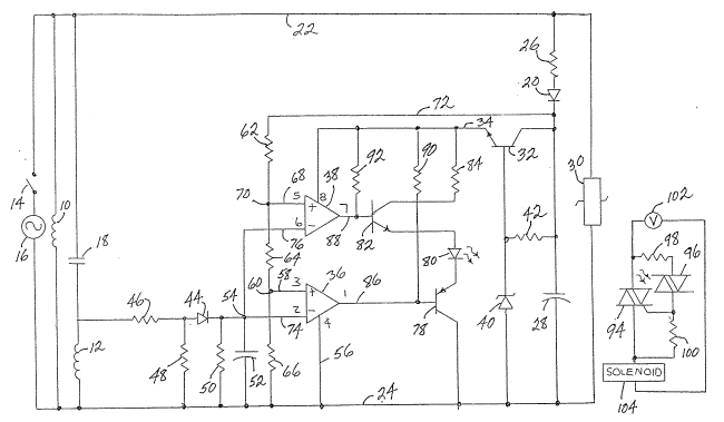
Referring to FIG. 1, a permanent split capaci-
tor motor has a main winding 10 and an auxiliary winding12 connectable through a main switch 14 to an AC power
source 16. Capacitor 18 in series with auxiliary winding
12 provides phase shift for starting and running torque.
A main voltage detector circuit including diode
20 senses main line voltage from AC sou~ce 16 across
lines 22 and 24. Voltage from ~C source 16 is sensed
through resistor 26 and half wave rectifying diode 20,
and filtered by capacitor 28. Varistor 30 provides
transient protection. An NPN bipolar pass transistor 32
has its emitter-collector circuit connected between the
cathode of diode 20 and line 34 which provides a regulat-
ed DC power supply voltage line for a pair of comparators


:

: . : :: .
. ' ' ~: . ~, :

7 ~ ~

36 and 38, to be described. The base circuit of transis-
tor 32 includes a zener diode 40 applying a limited
voltage from AC source 16 through diode 20 to the base of
transistor 32 to bias the latter into conduction. Base
drive current is supplied through resistor 42.
An auxiliary voltage detector circuit including
diode 44 is connected across auxiliary winding 12 for
sensing auxiliary winding voltage. The auxiliary winding
voltage is reduced by the voltage divider network provid
ed by resistors ~6 and 48 and sensed through half wave
rectifying diode 44 and resistor 50 and filtered by
capacitor 52, to provide sensed auxiliary winding voltage
at node 54.
Voltage comparators 36 and 38 are provided by a
~5 dual comparator integrated circuit, provided by an LM393
integrated circuit, where manufacturer assigned pin
number designations are shown to facilitate understand-
ing, having power supply voltage provided at line 34, and
are connected by line 56 to a common reference at line
24. Non-inverting input 58 of comparator 36 senses main
line voltage at node 60 as reduced by the voltage divider
network provided by resistors 62, 64 and resistor 66.
Non-inverting input 68 of comparator 38 senses main line
voltage at node 70 as reduced by the ~oltage divider
network provided by resistor 62 and resistors 64, 66.
The noted voltage divider network is connected by line 72
to the cathode of diode 20 and provides floating line
compensation. Inverting input 74 of comparator 36 senses
auxiliary winding voltage at node 54. Inverting input 76
of comparator 38 senses auxiliary winding voltage at node
54.
The emitter-collector circuit of a PNP bipolar
transistor 78, a light emitting diode, LED, 80, the
emitter-collector circuit of an NPN bipolar transistor
82, and a rPsistor 84 are connected in series between
lines 34 and 24. The base of transistor 78 is connected
to output 86 of comparator 36. The base of transistor 82


. .. .. :
.. ~


:~-: . : .

2 ~
-- 4
is connected to the output 88 of comparator 38. A pull-
up resistor 90 is connected between line 34 and compar
ator output 86. A pull-up resistor 92 is connected
between line 34 and comparator output 88. An opto-driver
5 switch is provided by a Toshiba TLP3012 integrated cir
cuit, including LED 80, power triac 94 and pilot triac
96. LED 80 is optically coupled to light responsive
element 96 to drive the latter into conduction to in turn
supply gate current through resistor 98 to the gate of
10 triac 94 to bias the latter into conduction. Resistor
100 reduces gate sensitivity and prevents false trigger-
ing. Triac 94 is connected in series with voltage source
102 and solenoid 104. Solenoid 104 provides a control
function, for example opening a gas valve in a furnace.
In operation, when auxiliary winding voltage at
node 54 increases as shown at 106, FIG. 2, above main
line voltage at node G0 as shown at level 108, then the
output 86 of comparator 36 transitions low, which biases
transistor 78 into conduction to conduct current from
20 line 34 through LED 80, which in turn emits light and
optically triggers triacs 96 and 94 into conduction, to
in turn energize solenoid 104. In FIG. 2, LED 80 transi-
tions at 110 from non-light-emitting state 112 to light-
emitting state 114. If auxiliary winding voltage contin-
25 ues to increase as shown at 116, FIG. 2, above the main
line voltage at node 70, as shown at level 118, then
output 88 of comparator 38 goes low, such that transistor
82 is rendered nonconductive which in turn terminates
current flow through LED ~0, and LED 80 transitions at
30 120 from light-emitting state 114 to non-light-~mitting
state 122 and hence triac 94 turns off at the next half
cycle of AC source 16, which in turn de-energizes sole-
noid 104. I~ auxiliary winding voltage decreases as
shown at 124 below level 118, then output 88 of compar-
35 ator 38 transitions hiyh to bias transistor 82 into
conduction to conduct current through LED 80, and LED 80
transitions at 126 from non~light-emitting state 122 to


.

~8~7~9
~ 5
light-emitting state 128, which in turn optically trig-
gers triacs 96 and 94 into conduction to energize sole-
noid 104. If auxiliary winding voltage continues to
decrease as shown at 130 below level 108, then output 86
of comparator 36 transitions high, to render transistor
78 nonconductive, which terminates current flow through
LED ~0, and LED 80 transitions at 132 from light-emitting
state 128 to non-light-emitting state 134, such that
triac 94 turns off at the next half cycle of AC source
16, to de-energize solenoid 104. When the auxiliary
winding voltage at node 54 is between levels 108 and 118,
LED 80 emits light (LED states 114, 128), and provides a
load-OK signal. If the auxiliary winding voltage is
below level 108 (LED states 112, 134), then motor speed
is too slow, and the load is too high. If the auxiliary
winding voltage is above level 118 (LED state 122~, then
the motor speed is too fast and the load is too low, e.g.
the fan on the motor shaft has become loose.
The circuitry senses first, second and third
ranges of auxiliary winding voltage and provides a load-
too high signal 112, 134 for the first range below level
108, a load-OK signal 114, 128 for the second range -
between levels 108 and 118, and a load-too-low signal 122
for the third range above level 118. LED 80 transitions
from the load-too-high signal 112 to the load-OK signal
114 to the load-~oo-low signal 122 as the auxiliary
winding voltage changes from the first range to the
second range to the third range. LED 80 transitions from
the load-too-low signal 122 to the load-OK signal 128 to
the load-too-high signal 134 as auxiliary winding voltage
changes from the third range to the second range to the
first range. LED 80 transitions twice as auxiliary
winding voltage varies from the first range to the third
range. LED 80 also transitions twice as auxiliary wind~
ing voltage varies from the third range to the first
range. LED 80 transitions twice during each of rising
and falling values of auxiliary winding voltage between


: .
. ~
:, :, -.

. - : . . .:
. .
: ~:.

2~8~7~
-- 6 --
the first and third ranges. Levels 108 and 118 vary with
main line voltage via connection 7~ and provide compensa-
tion of same such that sensed motor load generating the
load-too-high signal, the load-OK signal and the load
too-low signal is independent of main line voltage.
In the noted application, in the first range
below level 108, the load is too high and the blower or
fan motor speed is too slow to turn on the gas in a fur-
nace, and hence solenoid 104 is de-energi~ed, for example
to disable or inhibit a gas jet. In the second range
between levels 108 and 118, the blower motor load and
speed is OK, and hence solenoid 104 is energized, to
enable gas to be introduced. In the third range above
level 118/ the blower motor load is too low and speed is
too fast, indicating, ~or example, that the fan has
become loose on the motor shaft or some other event
causing loss or reduction of load, and hence solenoid 104
is de-energized, to disable the gas jet.
FIG. 3 shows a further and preferred embodiment
with hysteresis and improved tracking, and uses like
reference numerals from FIG. 1 where appropriate to
facilitate understanding. Resistor 140 and diode 142 are
connected between non-inverting input 58 and output 86 of
comparator 36. When comparator output 86 transitions
low, resistor 140 and diode 142 conduct current there-
through from non-inverting input 58 to output 86 and
lower the voltage at non-in~ert ng input 58 such that
auxiliary winding voltage at node 54 must decrease at
144, FIG. 4, to a level 146 below level 108 before com-
parator output 86 can transition high ~o turn o~f tran~
sistor 78, thus providing hysteresis. Turn-off of tran-
sistor 78 terminates current flow through LED 80, and LED
80 transitions at 148 from light-emitting state 128 to
non-light-emitting state 134. Diode 142 blocks current
flow from power supply voltage line 34 through pull-up
resistor 90 to non-inverting input 58 to remove the
regulated power supply voltage component from sensed main


' .; : ' , '
. ,... ,. ~

~: ~ , : -
., .

~8~769
- 7
line voltage at comparator input 58 This improves
tracking response of levels 108 and 146 to changing main
line voltage. Furthermore, main line voltage at compar-
ator input 58 is not offset by the regulated power supply
voltage from line 34. In the absence of diode 142, a
component of the regulated power supply voltage from line
34 through pull-up resistor 90 would be present through
resistor 140 at comparator input 58, and hence main line
voltage at comparator input 5~ would be offset by such
regulated power supply voltage. This is undesirable
because the regulated power supply voltage is relatively
constant, and does not vary with main line voltage.
Resistor 150 and diode 152 are connected be-
tween non-inverting input 68 and output 88 of comparator
38, and perform as above described for resistor 140 and
diode 142. Bipolar transistor 82 of FIG. 1 is replaced `r~.
by field effect transistor, FET, 154 in FIG. 3. FET 154
includes an inherent reverse diode 156. ~esistor 158
provides gate referencing for FET 154. When comparator
output 8~ is low, resistor 150 and diode 152 conduct
current therethrough from non-inverting input 68 to
output ~8 and reduce the voltage at comparator input 68
such that auxiliary windi~g voltage at comparator input
76 must decrease at 160, FIG. 4, to a level 162 which is
less than level 118 and greater than level 108 before
comparator output 88 can transition high to bias transis-
tor 154 into conduction, thus providing hysteresisO
Turn-on of transistor 154 conducts current through LED
80, and LED 80 transitions at 164, FIG. 4, from non-
light-emitting state 122 to light-emitting state 128,
which in turn optically triggers triacs 96 and 94 into
conduction to energize solenoid 104. Diode ~52 blocks
current flow from regulated power supply vol-tage lin~ 34
-through pull-up resistor 92 and resistor 150 to com-
parator input 68 to remove the regulated power supply
voltage component from sensed main line voltage at com-
parator input 68. This improves tracking response of


.

~ . .

'

~8~71~
-- 8
levels 118 and 162 to changing main line voltage. Main
line voltage at comparator input 68 is not offset by
regulated power supply voltage from line 34. Levels 146,
108, 162 and 118 vary with main line voltage via connec-
tion 72 and provide compensation of main line voltagesuch that sensed motor load generating the load-too-high
signal, the load-OK signal and the load-too-low signal is
independent of main line voltage.
Bipolar transistor 82 in FIG. 1 is replaced by
FET 154 in the hysteresis version in FIG. 3 to enable
comparator output 88 to remain high when the transistor
is conductive, to prevent hysteresis when undesired. In
FIG. 1, when transistor 82 turns on, there are only three
~unction drops from comparator output 88 to line 24,
namely transistor 82, LED 80, and transistor 78, and
hence comparator output 88 does not remain high. If
there were a hysteresis connection between output 88 and
input 68 of comparator 38 in FIG. 1, the voltage at
comparator input 68 would be reduced by such connection,
even during rising values of auxiliary winding voltage
when auxiliary winding voltage at comparator input 76 is
less than main line voltage at comparator input 68,
because conduction of bipolar transistor 82 across its
base-emitter draws comparator output 88 low. FET 154 has
an insulated gate as a control terminal, and hence when
output 88 of comparator 38 transitions high in FIG. 3,
such output 88 remains high, such that the voltage at
comparator input 68 is not reduced by the connection
through resistor 150 and diode 152 during rising values
of auxiliary winding voltage when auxiliary winding
vol`tage at input 76 is less than main line voltage at
input 68, thus preventing hysteresis during such inter-
vals. Instead, hysteresis is effective only during
decreasing values of auxiliary winding voltage when
auxiliary winding voltage at input 76 is greater than
main line voltage at input 68 and comparator output 88 is
low.


~ . . .
.. ~ -
,,, ~" , ~ ,:,

7 6 ~
g
In another embodiment, transistor 82 is re
placed by an SCR connected in parallel with LED 80 and
transistor 78, and shunts current away from LED 80 and
provides latching of LED 80 in the non-light-emitting
state 122 if an overspeed condition is detected.
It is recognized that various equivalents,
alternatives and modifications are possible within the
scope of the appended claims.


.~: -


: ~ ,
-

Representative Drawing
A single figure which represents the drawing illustrating the invention.
Administrative Status

For a clearer understanding of the status of the application/patent presented on this page, the site Disclaimer , as well as the definitions for Patent , Administrative Status , Maintenance Fee  and Payment History  should be consulted.

Administrative Status

Title Date
Forecasted Issue Date Unavailable
(22) Filed 1993-01-06
(41) Open to Public Inspection 1993-07-28
Dead Application 1995-07-08

Abandonment History

There is no abandonment history.

Payment History

Fee Type Anniversary Year Due Date Amount Paid Paid Date
Application Fee $0.00 1993-01-06
Registration of a document - section 124 $0.00 1993-07-09
Owners on Record

Note: Records showing the ownership history in alphabetical order.

Current Owners on Record
CHMIEL, STEVEN F.
REXNORD CORPORATION, STEARNS DIVISION
Past Owners on Record
None
Past Owners that do not appear in the "Owners on Record" listing will appear in other documentation within the application.
Documents

To view selected files, please enter reCAPTCHA code :


To view images, click a link in the Document Description column. To download the documents, select one or more checkboxes in the first column and then click the "Download Selected in PDF format (Zip Archive)" or the "Download Selected as Single PDF" button.

List of published and non-published patent-specific documents on the CPD .

If you have any difficulty accessing content, you can call the Client Service Centre at 1-866-997-1936 or send them an e-mail at CIPO Client Service Centre.


Document
Description 
Date
(yyyy-mm-dd) 
Number of pages   Size of Image (KB) 
Drawings 1993-07-28 3 84
Claims 1993-07-28 10 534
Abstract 1993-07-28 1 31
Cover Page 1993-07-28 1 22
Representative Drawing 1999-08-03 1 19
Description 1993-07-28 9 474