Note: Descriptions are shown in the official language in which they were submitted.
92/22877 1- P~r/US92/03766
TEMPERATURE-INDEPENDENT LINEAR-TO-
EXPONENTIAL CO~IV~;~
Ba.,l~luulld of the Invention
The present invention relates generally to linear-to-
al converter circuitry, and, more particularly, to a
0 i~ l~pG~ AALUl G; ~ /i . ni Iinear-to-, ~ 1 converter capable of
li; Gll G~ g a 1~ Al l,U Gl A i~ U~ 8ignal whi ch i 8
related to an input signi31 applied thereto.
Many types of circuitry utilize linear-to-~a~AnnantiAl
circuitry to generate a signal which is ~ ly related to an input
5 signal spplied thereto. For instance, circuitry for_ing portions of
c ~ of a ~ system ~ one such type of
circuitry which r l~_"~ o lcly utilizes such linear-to ~
circuitry. Ty~pically, when linear-to ~ l- --.r..l:cl circuitry forms portions
of such rnlnmllnir~f;An, ' the linear-to-~ 1 circuitry
20 is utilized to convert linear-scaled signals into decibel-scaled signals. (A
decibel is a value related to an ~ 1 value.)
A Ll A~ and a receiver comprise the ~ I portions of
a ~ .. ; -1: --~ æystem. The Ll~ulDA~uLLGl aA~d the receiver are
illk.. ~..",~ d by a L1A~-L-..~ n channel, and an ;,.r... ~ signal is
25 L1A-~L~ d by the tlc~ iLh,~ upon the L~ channel to the
receiver which receives the Ll '' 1, infA~rmAtinn signal.
A radio, "^- system r ..~ a
;I)II system wherein the L1A~I .. L.' ... channel is formed of
a radiO LG4UGll-~ romml~niratinn channel. The radio-frequency
30 rn~nml1nirAtinn channel is defined by a range of frequencies of the
~le_Ll....'AenP~ LGU,UG11L~ spectrum. To trans~nit an illrUllu~ti
signal upon the radio-L~uG.l~ rnnnmllniratinn channel, the
wO 92/22877 2 0 8 7 i 2 2 PCI/US92/03'O
infnrmotion si~nal must be converted into a form suitable for
tronRmir~;on thereof upon the radio~Lc~lu~."~ channel.
Cu~ ;u~ of the inf^~mo~i ~n signal into a forrrA suitable
for L~ thereof upon the radio-rl~qu~
channel iB ~ d by a proce3s referred to as rA~d~lst;on wherein
the il ru. "n sii~nal is , ~_3~ upon a radio-r.G~u~
~Ic~LI - ~ :c w~ve. The radio-LG~u~ L-.~...... s~cllPtic wave iB of a
value within a range of rle~uellcies of the L~lu.,..~6 which define the
radio-rl~u~ m channel. The radio-r~qu~
0 ~ o~ ot;~ wave upon which the inf~rmotinn signal is h~ 3cd
i3 commonly referred to as a "carrier signal", and the radio-r.G~Iue~
~Ic~L-~ ..9~ wave, once ~ lot~od by the inf~rmoti~n signal, i8
referred to as a mn~-llotPd signal.
The information content of the ---~-l--l~i- d signal occupies a
5 range of r ~qv~ referred to aO the ~ lot;on
spectrum. The range of rl~,quel.c;c~ which comprise the mn;l-lotion
spectrum include the LGqU.~ of the carrier signal. Because the
- ~ lotPd signal may be i ' through free space upon the radio-
LG~uel~ channel to transmit thereby the i. rul~AALi~,.. signal between
20 the transmitter and the receiver of the radio c- ~ sy6tem, the
1.. ~.. ; I ~-. and the receiver portions of the ~.. , .. ~ ~ :~n system need
not be pQ~iti~mPd in close ~-u hlliLy with one anot,her. A3 a result, radio
,.. ".. ";rotinn systemg are widely utilized to PffPCtllotp ~.. --.. _I ~n
between a L~A uAiLL. ~ and a remotely-pnciti~nPd receiver.
Various . -ur~ have been developed to
modulate the infr,~oti~,r. signal upon the carrier signal to form the
mn/ll~ pd signal, thereby to permit the L ~ ' of the ;, f
signal between the L~ P~LL~. and the receiver of the radio
c~ n system. Such rA~dl~l ' nn tPA-hniq~PR include, for
e~ample, A---l-l;l--AP -G-l lAi: - (AM), r.~qu~ n~n;"lAt;Qn (FM),
phase mndlllot;A,~ (PM), r.G~Iu~ , hift keying m^dl~loti~n (FSK),
phase-llhift keying mo~ loti~m (PSK), and ~ - .1;... - - ~ phase mn;lllotinn
~jO 92t22877 2 0 8 7 ~ 2 2 Pcr/US92/03766
(CPM). One type of - -- .t~ c phase .----~ i6 ~ LU~G
,~nrlit7~AP mn~ t;~n (QAM).
The receiver of the radio l system ~vhich
receives the ' ' ' signal contains circuitry to detect, or to recreate
5 ulL_.~iDe, the i~r~ Lu~ signal ~r~ upon the carrier signal.
The circuitry of the receiver typically includes circuitry to convert
du..~ in LG~ G~ the r~7~ tPd signal received by the receiver in
addition to the circuitry required to detect the ;. ,r . . - ~: . signal. The
proces6 of detecting or .~_....Lu.g the ;"f--. --~:-... signal from the
.7~n~ tPd gignal ig referred to as dpnn~ lllDt;nn~ and such circuitry for
p~.ru~Lh~g the r3Pn n~3lllDt;~n is referred to a6 d~ . circuitry.
In 60me receiver CO~QI~U~LUnQS~ circuitry including a
pr~,cessor (referred to a6 a digital 6ignal processor or a DSP) i6
Q~llhQt;tlltPd for ~u~ G..~io..A~ ~ 1 circuitry.
The signal actually received by the receiver of a radio
~.. 1.lll . I:~n 8y8tem r.. ~luG.. IlY varie6 in ~ '- as a result of
reflection of the 1. d signal prior to reception by the receiver.
Typically, the signal actually received by the receiver is the ~
of the ~ J?d 6ignal ~vhich travels along a plurality of different
20 paths forming signal paths of differing path lengths. Because the
tranQmi~;on channel upon which the nnr~ tPd 6ignal is f,-
typically includes a plurality of di~ferent signal paths, a ~
channel i6 L~ U~IIY referred to as a multi-path channel.
T - of the signal upon 6ignal paths of path lengths greate~
25 than the path length of a direct path result6 in signal delay as the
gllmm~t;~n of the ~ signal upon the multi-path channel is
actually a D~ ' " ' of siAFnal 1- A ~ I t d by a IIA - ---' -' I I ~ and
received by the receiver at different points in time.
Such signal delay results in inL~If~l G.~ G referred to as
30 Rayleigh fading and intersymbol i~LG~rG~GncG. Such illl~.r~ e ca~se6
6ignal _mrlih~llP variance of the signal received by the receiver. When
the ~v ~ sy6tem, formed of a l~ and receive~,
WO 92/22877 Pcr/US92/
21~8~522 4
comprises a Lr~ and receiver of a mobile ~ system
(such as a eellular I~l~Auhu~li system), when a reeeiver is pc~ .P~l in a
vehicle traveling at 60 MPH, the signal strength of a ~o~ l signal
L 3l' by the LlculDL IiLL~ and aetually reeeived by the reeeiver,
5 may vary by cl,u,uluAi~Lely 20 decibel6 during a five m~ pcrn~ period.
Gain eontrol cireuitry il~ form6 a portion of the
receiver eireuitry al~. uaLely to amplify the received signal and limit the
m~nitll~P of the received signal to overcome the effects of such fading.
Gain control eircuitry typically utilizes signals whieh are
0 scaled in terms of deeibels per volt. A6 a deeibel is a lc~ c value,
linear-to ~ I-h-~. .~l ol CUll~.D;i~ll eircuitry also typieally forms a portion
of the gain control eircuitry of the rec_iver cireuitry.
EAisting linear-to I A~ -r -1 ~1 Wll~..DiUII cireuitry is
available which i8 operative to form an ~.l.. ~I G1 output 6ignal
~i leD~JUllDiV~ to ~r~lirs~ n of a linear input 6ignal thereto.
For in6tance, disclo6ed in a text entitled, "IC Op-Amp
Co~ r " by Howard W. Sams, copyright 1974, page6 214-216 is an
antilog ~ .c Lu- for for_ing an ~ l------ ~I nl signal IlE,..~JUl~Di~, to
~rrlirPt;r~n of a gignal thereto. The antilog ~ eL t .aL... is ~ 1 of
20 discrete ~
Also, an ;~IL L~ "d eireuit, INTERSIL Part No. ICL8049,
discloses a similar such 6tructure in ` ', '~l eircuit form.
A--iAitj~n~lly, an integrated eircuit, INTERSIL Part No. ICL8048,
discloses a l~,i"~ 1 ;r converter for ~.fU~LUillg a lui~;Ll~c
2~ conversion.
The eAisting eircuitry for C~ ulg an r ~ :ol signal
,uU118;V~ to arrlir~t;~n of an input signal thereto form6 an .I....,_..I:nl
signal which is t~ pt laLul~ riPpPn~3Pnt The aetual signal i~eL i .c L~d by
such circuitry is therefore t~ uu~ Lult~ J~ .,l, viz., the actual,
30 f ~l..~.,_.~i:'l signals gt~-lc.ai~d by sueh cireuitry are of values vrhich vary
~;ul._,~l----.~in~ to the l~u~,.ai,Ult~ of the eireuitry. Therefore, the
signals ~ alêd by such existing cireuitry are not ~ . solely
~o 92/22877 2 08 7~2 2 PcrtUS92/03766
upon the values of the signals supplied thereto, but also upon
k ul.~.6Lu~..
While both the antilog 6~ ~.d~u~ and the i..t~t,.e.~ circuit
equivalents thereof attempt to provide ~ , c.Lu.~-c~ . to
minimize the A~ of the signal formed by the circuitry upon
., t, such attempts ~nay not totally caneel the 1~ Lu~
A. "~ of the liignal.
The antilog 6~,~.~Lu. disclosed by Sams includes a discrete
l.. ;~ ~, . As the ~ . e of the IJ~ ~, i8 not npc~qc~rily
0 equal to that of the ampli~ier of the antilog generator, the attempt to
r~ . for the k...p_.c.Lu.~ r of the signal is frequently
ins~ PqU~tP
The antilog 6~ Lu~ disposed upon the illk6.6l_d circllit
attempt~ to ~ for the t~ u~.6Lu~ of the signal
5 6~ kd Ll._. ~L, by forming the; 1 l IL Ll ~ lPA circuit by a hybrid
production process. An ;..t. 6.~1-.l circuit formed of a hybrid ~.udu~iu..
process is of at least two different types of ms~t~ri~lc Such a process
increases ~ulu~,LiG~ costs as well as material costs, and, in any evellt,
the l,_ u~ Lu~ -. circuitry of such illt~",..lL_d circuits
20 ag~un may not totally cancel the ~ ..,u.,,~.~u.~ . The attempt
to ~ for the klu~ Lul~ in this manner is,
therefore, r.~U ,.LIy; I.Q~F~
Ac~,u.LI.~ly, gain control circuitry of receiver c~--.l.. l .. I`;
of a radio rn~nnlunir~tinn system which utilizes such conventional
2s linear-to-~ l Cull~_.Di~"l circuitry 6_.,~.--te_ signals which vary
CUIl-~ e to the ~.~ Iul~ level of the circuitry. Therefore, gain
control signals 6~ L-d by such gain control circuitry are, at least in
part, variable l~ UII/~ . to i , ~.Lul~ levels. As such 1~ I~elc.Lul~
A_~, ..~1.... ~ adver8ely affects the filnrtinnine of the receiver gain control
30 circuitry, the resultant g~un control of a received signal is subject to
error.
~` 2087522
- 6 -
What i6 needed, therefore, is linear-to ~ .l.,,.._..~:ol
Cullv~uAiu~l circuitry which ~ullul~I,es an P~nPntiol signal which is
uiue~l,ul~-in~lPpPnrlPnt
S Surnmary ûf the Inventiûn
~ he present invention, therefore, Ldv~ ouOly provides a
circuit fûr ~ r~ tillg a l~...~ -;..rl~lJ .,~l_.,l Oignal which is
Dlly related to an input signal.
rlA-he present inventiûn further LdV~ uAly prûvides a
methûd for ~-:u~.~Lillg a L~,ue.~A~ult-in~ "~ signal which is
~,1.. ,I:~lly related to an input signal.
The present invention yet further rAIv~ ",~ u ~ ~Aly provides a
linear-to-~ ol converter for a gain control circuit ûf a radio
5 receiver which ~.~ rl~o a tb~,Url~ul~ inrlprpn~lpnt bias current
which is ~,l.. l: Dlly related to a control vûltage.
rlA-he present invention still further r.~vA ~ , u~ ~Aly provides
a circuit for tll~.rALillg a signal which is lrl~r-;~ Ally related to an
input signal.
'lAhe present invention provides further adv~lL~ t O and
features, details of which will become more apparent by reading the
detailed rl~ ûf the preferred ~ -o-l;.. l-~ hereinbelow.
In accordance with the present mvention, there is provided a circuit fûr
generating a 1~ 8~ dc~-ldc~-L signal which is p~rr)npn~ ly related to an input
25 signal. The circuit comprises a t~ aLu~ l l amplifier and an
P~-~nPn~i:,l amplifier. The Ltlll~)~,.d~UlC- , amplifier has at least one band-
gap current generator operative to generate a current of a value proportional to~tlll~ ,ld~UlC. The t~ dLulc-~ , amplifier is coupled to receive the input
30 signal, and operative to amplify the input signal and to generate thereby an amplified
signal of a value ~UIU~!UILiU~dl to Ltu-~.dlu-c. The exponential amplifier inclLIdes at
least one bipolar junction transistor having a base electrode, a collector electrode, and
an emitter electrode. The base electrode of the at least one bipolar junction transistor
is coupled to receive the amplified signal of the value ,ulu~ollicl~dl to Lt~l~p~ Id~UlC
generated by the t~.U~ld~UlC-C~ ) . amplifier. The amplified signal is
. , .
2~8~522
- 7 -
operative to bias the at least one bipolar junction transistor at a bias voltage of a value
which is ~IIU~ iVII~II to h~ whereby a current generated at the collector
electrode of the at least one bipolar junction transistor is c~, 'Iy related to the
5 bias voltage of the base electrode of the at least one bipolar junction transistor. Thus,
the current generated at the collector electrode of the at least one bipolar junction
transistor comprises the i ~ signal which is exponentially related
to the input signal.
0 Brief D~ .. . of the Drawings
The present irlvention will be better ....-1 ,~ ~vd when read
in light of the P ~ y;llg drawings in which:
FIG. 1 is a graphical l.,e~ n of the current
s generated at the collector clectrode of a bipolar junction L~ ;sL
plotted as a function of the base-to-emitter voltage thereof at three
different ambient tG~ G~ G levels;
FIG. 2 is a .~:",~ P~ block diagram of the circuit of a first
preferred Pmhvrlimpnt of the present invention;
FIG. 3 is a block diagram, similar to that of FIG. 2, but of
an alternate preferred ~ bv l;~ i of the present invention;
FIG. 4 is a fiow diagram listing the method steps of tlle
method of a preferred I ...h.~.l;...~..l. of the method of the present
invention;
FIG. 5 is a ~imrlifipd circuit diagram of an impl^ nP~t~tinn
of the preferred ~mhorlimPnf of FIG. 3;
FIG. 6 is a ~. 1,. .. 1 :~ view of a portion of a cellular
cnnnm~1ni~Pti~n system;
FIG. 7 is a graphical lG~JI' ~ -.1`-1 "'~ of a mod~ t~d ~ignal
30 plotted as a function of rlG~Iuell~ ~,
FIG. 8 is a block diagram of a radio L1UI1~CG;VGI havir, g a
receiver portion of which a linear-to ~ circuit of the present
invention forms a portion thereof;
FIG. 9 is a block diagram of another P~ltPrnP~t~ preferred
Pmho~limPnt of the present invention which for_s a 4 lI~ IIIG
inclPpPnrlPnt, lo~ ,L,.~ signal;
.,_
~o 92/22877 2 0 8 7 ~ 2 2 PCI-/US9Z/03~
- 8 -
FIG. 10 is a block diagram of yet another ~ltPrnqtP,
preferred .h~ . of the present invention ~vhich forms a
u~G-inAPppnApnt~ signal; and
FIG. 11 is a fiin~rlifipd circuit diagram of the preferred
~ .G~ of FIG. 10.
D~ of the Preferred ~hoAimPnfc
Turning first to the graphical ~ v ~ of FIG. 1, the
0 current {~GlI._.~lkil at the collector electrode of a bipolar junction
~ u~D;Dt-v~ is plotted as a function of the potential li~ G across t~le
base arld the emitter el~_L-ul~O, VBE, of the bipolar junction l-~D;oLv~.
The collector current, Ic, scaled in terms of n~illiqmrPres~ is plotted
upon ordinate axis 20 as a function of the base to emitter voltage, VBE.
5 scaled in terms of millivolts on abscissa axis 24.
Plots 28, 32, snd 36 represent the l. 1 ~ :- . RI.;1- betvveen the
current at the collector electrode and the voltage across the base-to-
e_itter ~ 1.. udeD of the bipolar junction 1~. at three different
klU~JGlal.UlG8--T2, Tl, and Tû, .~ e~ ly, vvherein T2 > Tl > To-
~Yqmi- of plots 28, 32, and 36 indicates that the current at a
collector electrode, Ic, of a bipolar junction ~ is d~ .A 1 not
only upon the base-to-emitter voltage, VBE, but also upon the
k..ll,G.aiuue of the ~ UD;DI,VI. For instance, at a particular base-to-
emitter voltage, indicated in the Figure by vertically . I .,1; . ~ line 40
25 shov~n in hatch, the current at the collector electrode of the LI~UD;DtVI
will be A~PpPnAPn~ upon the tGlUp~ tUlG of the 1~1 . At
k.u~ u G T2, the current Ic at the indicated base-to-emitter voltage is
indicated on the curve by point 28A. At k u~el~ult Tl, the current Ic at
the indicated base-to-emitter voltage is inAicated by point 32A, and at
30 t~ lOtUIG To, the current Ic at the indicated base-to-emitter voltage,
VBE, is indicated by point 36A.
~!0 92/22877 2 ~3 8 7 5 2 2 Pcr/US92/03766
Similarly, for a larger 1 - ~r l voltage, VBE.
indicated in the Figure by vertically ~ e line 44 shown in hatch, at
L~ ~ T2, the current Ic at the indicated base-to-emitter voltage is
indicated on the curve by point 28B At ~ Tl, the current Ic at
5 the indicated base-to-emitter voltage is indicated on the curve by point
32B, and at i , ' . To, the current Ic at the indicated base-to-
emitter voltage is indicated by point 36B.
Plots 28, 32, and 36 may be ' lly degcribed by the
following equation
0 Ic = Ijat enBEq/kT)
where:
Ic i8 the current level of the current at a collector electrodeof a bipolar junction 1,1.- I~i,,~l,
Isat is the D_Lul~Lull current ~ ': of the bipolar
5 junction Ll~O:sLul,
e is the value 2.71 (wherein In(e)=l);
VBE is the voltage level taken across the base and emitter
L.udes of the bipolar junction Ll~oioL~
q is the charge of an electron;
k is R~ '8 constant; and
T is the t ~ of the bipolar junction L ~,oioL
(scaled in terms of absolute degrees)
The above equation shows . ~ll I A11Y, and, plots 23-36
of FIG 1 show graphically, the ~ of the current
25 at the collector electrode of the bipolar junction L with the base-
to-emitter voltage, VBE, of the L~ o;oLul The above equation also shows
lly, and plot8 28-36 of FIG 1 also shows graphically, the
Lt ~ Lul ~ of the current at the collector electrode of the
Ll~lsiOLu~ with the L~ Lul~ thereof
Because of this t~ ._Lul. ~ J, the signals
._I,cd by w..~.;.lLiu..al linear-to-~ 1 circuitry require
t~ Lul e C ~ n
WO 92/22877 Pcr/uss2/o37~
208~S~2
- 10 -
Turning now to FIG. 2, the circuit of a preferred
' of the present invention, referred to generally by reference
nurneral 70, is 6hown. Circuit 70 generatvs a ~ u~ Lu
signal which ia ,I - ,_..l;Ally related to an input signal.
An input signal formed on line 74 is supplied to
v ~ . circuit 78 . T~_. _ Lul v
circuit 78 is operative to convert the input signal supplied thereto on line
74 into a lvllll~_.6~ul~. A- I~- .At- -~ aignal of a deaired l ~ ' - v
At-lJ. .~ . With reference to the ~,-v. ~,-listed
0 equation u~ed to describe the current at the collector electrode, Ic~ circuit
78 i8 operative to introduce upon the signal supplied on line 74 a
_i.UI V ~1. " . ~A.... J which is inverse that of the ~ , v
t~ J of the above-listed equation.
T~ UIV ~ , ~rm circuit 78 gPnPr~tPA a
L_AIIIJ_~AALUIV-A~ IJ .A~ .~ signal on line 82 which is coupled to -
~mllltirlipr circuit 86 to supply the I -~ I signal thereto.
F.. ~ .~.. 1: -1 r-A-~lltirlipr circuit 86 .. - .. n~ 1~ at least one bipolar junction
~._I.a.bl~, which forms an _,1 ,I al _.~.I~l;r'. Al ~ circuit. Because,
as ~ iU~Dly described, the current at the collector electrode of the at
20 least one bipolar jurlction ~ D;D(~ is -~ lly related to the base-
to-emitter voltage thereof, the current at the collector electrode form~ an
I ~lly-amplified signal L~ lDi~ to a signal applied to bias the
base electrode thereof (here the aignal supplied on line 8a). A signal
g_~CA ' ' on line 90, which is ~ ~y coupled to the collector
25 electrode of the bipolar junction L.- -ID;S~ of multiplier 86, is
lly related to the input signal supplied on line 82. Because the
L_.lll~_~_LU V~~ t signal g_AI_A_LOd on line 82 is of a 1- ---1 ~ e
rlPrPnAPnt y inverse to that of the 1, . .1.. . ,- ' . v ~1_l, ,A_- ~ of the at least
one bipolar junction Lll DiDL~ the signal generated on line 90 by circuit
30 86 is t~VlUIJV- AA-.UU v-invariant.
Turning now to the block diagram of FIG. 3, a circuit,
referred to generally by reference numeral 100, of an alternate preferred
~lo 92/22877 2 0 8 7 5 2 2 Pcr/uss2/o3766
_...h.,.l;,....~ of the present invention is shown in filnrhr~n~l block form.
Sirnilar to circuit 70 of FIG. 2, circuit 100 is operative to generate a
t_ u,u.,~ALulc~ A~ A- ..1. signal which is --~u~ lly related to an
input signal supplied thereto. More particularly, circuit 100 of FIG. 3 is
operative to receive a voltage signal which forms an input signal and to
generate a k~ l.u o ;--A~ .1- current signal which is
, ~ -'ly related to the voltage level of the voltage signal formin~ the
input signal.
With reference, then, to the block diagraln of FIG. 3, a~
input signal, formed of the voltage signal, is ~ ' on line 104, ~nd
supplied to voltage-to-current converter circuit 108. Voltage-to-current
converter circuit 108 converts the voltage signal supplied thereto on line
104 into a signal of a current of a level which varies ~ U~-D;~C to the
level of the voltage of the voltage signal forming the input signal. The
current signal forrned by converter 108 is b~ .c.kd on line 114 whi~h is
coupled to t~ U~U~ UI~ circuit 118 to supply the current
signal thereto. T , ~U.O ~ - -I-_ .~-l rn circuit 118, siilar to
~ u~uO.rA~u. O ~ ': --. circuit 78 of FIG. 2, is operative to introdluce
a desired kl.lu~ Lulc ~ A. --.~ upon the current signal supplied
20 thereto on line 114, and to generate a t~l-- _~- .~ A- ~ A~ currerlt
signal on line 156.
Line 156 is coupled to ~ al ~- 1 l ;l-l; circuit 160.
"~"~"":nl rr~lltirliPr circuit 160, gi_ilar to ~ 1 mllltirli~Pr
circuit 86 of FIG. 2, is operative to generate a signal, here on line 170,
which is _A~ ly related to the signal supplied thereto on line 156.
Si_ilar to -.l.. ~ :~l mllltirliPr circuit 86 of FIG. 2,
circuit 160 of FIG. 3 ~rriRPs at least one bipolar junction Ll~_ D~U~
which forAns an ~ l Amrlifir~ti~n circuit. The current at t~le
collector electrode forms an P-rnnPn~i~lly-amplified signal lC~.~JUIm;llo to
a signal applied to bias the base electrode thereof (here, the signal
supplied on line 156). Line 170 is ~ ù~u.; Akly coupled to the collector
electrode of the Ll ~IDiDLUI and the current at the collector elOctrode of the
WO 92t22877 Pcr/US92/037
2o87S2~ - 12 -
L. , and the current at the collector electrode forms the output
sihnal on line 170 which is ~ ly-relat~Od to the input signal
supplied on line 156 Similar to the . ~ ' ' between L~ Lule
circuit 78 and ~ l n--ltirliP- circuit 86 of FIG 2,
Lo~ ulc t.~ " circuit 118 and ~ .I.r.. ~l a7 ml-ltirliPr
circuit 160 of FIG 3 are I ~ l~kod in that the L .~ . pLul O ~ " . A~
h.LIulu~cd upon the signal supplied to circuit 118 on line 114 is inverse
to that of the l~ Lul e A- ~ ,A- -- / i--L u lu o~ upo~ the current
generated at a collector electrode of the at least one bipolar junction
0 Ll~ulD;DLul of r~ -l m~ltirliPr l6o Because thO tO~"~ Lu
APrPnAPnt gignal h_.._.~.~d on line 156 is of a L ~ Luuo ~ -A- ~
invOrse to that of the tOII~ O A- IJ -A- .,. .~ of the at least onO bipolar
junction Ll of circuit 160, the sign~ d on line 170 by
circuit 160 is i aLu.~ invariant Because of such t l.- ..I .e-
15 illvc.l;a l~o, the signal ~.l~ ud on line 170 does not vary l~ UIID;~_ tochanges in ambient k~~ .Lulo
Turning now to the flow diagram of FIG 4, the steps of the
method of a preferred: ~ ' of the present invention are listed for
D_.l .~Li~.g a Lclu,u_.c~Lu~ AI ~ signal which is ~ lly
20rOlated to an input signal
First, and as indicated by block 178, the input signal is
converted into a L~ Lul~ A~ i signal of a desired L~ ule
~. ~,..,A.... ~. With respect to the filnrt;~nnl block diagrams of the
prPrerred; ' ~ of FIGs 2 and 3, L~ I e ~.. I.. ~.. ~-I.;I~n
circuits 78 and 118 of the l~ Li~_ figures are operative to perform such
a step.
Ne~t, and as indicated by block 182, the l~ Iuue-
d~ l sihnal is amplified by an ~ l al ml~lt.irli~Pr having a
Lclul,_.pLu o d~ A .-~ v (.u,-- ~ to, and inverse of, the
t~ Lu- 6 d~ of the L_~e~Luu~ A- .~1 signal such that
an amplified signal formed thereby forms the L~u~ Lule-i~ A l~ t
signal which is ~.~.n.,. " -lly related to the input signal With respect to
~10 92r22877 1 3 PCr/US92/03766
the preferred: ~ ' of FM6. 2 and 3, such step is p- f~ d by
P ~ ltirliPr circuitg 86 and 160 of FIGs. 2 and 3, l~ w._l~.
In a preferred: ' ' of the method of-the present
invention, the step of .,v... _. w-.g the input signal into a ~._. .. Lule-
5 A~ ~J - r~ 1 signal; , the step, indicated by block 186, of
~v..~_. Li- g the input signal into a signal having currents of levels which
vary l~ U~D~, to values of the input signal. With respect to FIG. 3,
such a step is p~ ~ - ' by voltage-to-current converter 108.
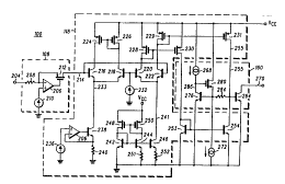
FIG. 5 is a circuit diagram of circuit 100, which was
previously shown in r.. I -.A1 block form in FIG. 3. Voltage-to-cu~^rent
converter 108, ~...~ Ul~,; . '- circuit 118, and ~
"" ~ ; circuit 160 i~ .d in the filnrt;~mAl block diagram of FIG.
3 are indicated in FM. 5 by similarly-~lu llb_.c~ blocks, shown in hatch.
Line 204 of FIG. 5 cv...,_,,v..v~ to line 104 of FIG. 3, and supplies an
input signal to voltage-fo t,~.. ~ converter 108. Line 204 is coupled to a
negative input of amplifier 206 through resistor 208. A DC voltage
"_.le.cLLl_d by voltage generator 210 is supplied to a positive input of
amplifier 206. Metal o~ide - ' field effect LIOIIDiDLV~
(MOSFET) 212 iuL~.wllll~_lD an output of amplifier 206 and the negative
20 input thereof. More particularly, and as illustrated, a gate electrode of
MOSFET 212 is coupled to the output of the amplifier 206, a source
electrode of MOSFET 212 is coupled to the negative input of amplifier 206,
and a drain electrode of MOSFET 212 is coupled to line 214. The signal
~_.l_. ' 1 on line 214 i8 of a current level which varies in value
25 ~,v, l ~ .I..,. ,.l; "~ to the variance in value of the voltage level of the input
signal supplied on line 204. Line 214 of FIG. v ~ _rlV11~8 to line 114 of
the filnrti~nsl block diagram of FIG. 3.
TC~ dtUI~ . ' ' circuit 118, in the preferred
~- " ' of FIG. 5, is ~vl.l~ d of a ~ ' wv.~ ' -- L;v.
30 amplifier and a band-gap current 6_~ Lvl. The
~1~ ' Lion/yf ~ - L;u.. amplifier forming a portion of ~ t . ,. LU~ ~
- " circuit 118 cv .1,l;.. _~ bipolar junction Il~llDi~t.vlD 216, 218,
Wo 92/22877 Pcr/uss2/o37~
2o8~522
- 1 4 -
220, and 222. (~ollector el~-Ll udG& of the ~ L -1~' :. 216-222 are
coupled to drain ~l~cL ud~D of c~ ones of MOSFETs
224, 226, 228, and 229. MOSFETs 224 and 226 are ~ ' "" -lly coupled
tu~GLller to fonn a current urror. Similarly, MOSFET 228 is
coupled to MOSFET 230 to form a currGnt mirror, and MOSFET 229 is
coupled to MOSFET 231 to forln a current mirror.
Voltage source 232 biases the base el~ ~,u~3 of ~ u ~$
218 and 220.
The ernitter F~ V~3 of ~, ' D 216 and 218 are coupled
together by line 233. Line 233 is also coupled to an amplifier circuit
" A~ d of amplifier 234 in which a voltage generated by voltage
source 236 is supplied to a positive input thereo An emitter electrode of
1~ - 238 is coupled to a negative input of amplifier 234: The emitter
electrode of L 238, and the negat*e input to arnplifier 234, are
coupled to ground through resistor 240.
The emitter el~,_l,iudG3 of i ' D 220 and 222 are coupled
together by line 241. Line 241 iB also coupled to to the band-gap current
generator ~u .~,I;..Fd of l,~ D;DlUlD 242, 244, and 246. MOSFETs 248 and
250, also ~ e a portion of the band-gap current b_.~ lul, are
coupled t~ ub_tl-er in a current mirror ~u lfibul~;ull. Drain
el~_.,rudes of the l~ i._ MOSFETs 248 and 250 ar~ coupled to the
collector Cl~_LLU~A of ~-~lsiDLulD 242 and 244, ., . ~GIy. Emitter
clF_~.udes of LI~ID;5L~IID 244 and 246 are coupled to ground through
resistors 251 and 252, ~ _ly.
2s The drain electrode of ~ DiDLUI 230 is coupled to the
collector electrode of Ll~rDiDLùl 253 which, together with i.l~Ul~ ,UI 254,
forins a current mirr~ir.
A ratio formed of the current levels on lines 241 and 233 of
the J,~G' Lion/,uoDLLD~uli.ion amplifier of t~ up_.aLulG ~.. .-, - ., -I:~.,
circuit 118 forms the gain of the amplifier. The current level on line 241
is, however, A~,u~--~i- ..~ upon the current level of the band-gap cunrent
b-.l~ due to the -- -F~ ~ U~ ~ of line 241 to the collector electrode of
~092/22877 PCI/US92~03766
208~522
-15-
L - ~oioLu~ 246. Therefore, the resultant gain of the
~u-~liOLul Lion/l,uOIL61u~ Lion amplifier is ~1. " ~A l~ upon the current
level of the band-gap current 6_.~ 1u~. And, because the band g;ap-type
current 6_.._._Lùl forms an output current at the collector electrode of
5 L 246 which is i _lu~ ,A- .l., the gain of the
1~ ' Li~uo;dioLu~ Lu~l amplifier is therefore also ,1~". ..~3. .1. upon
- Lu~
The p~eLol,u~Liu~old;o~ulLu~l amplifier ~,_.I_._Leo an
nplified si6nal, formed of the D"l"l--` 1 "" of the current at the drain
electrode of MOSFET 231 and the current at the collector electrode of
Ll 254, I~,Lr~u~o~., to ~ of the input 6ignal supplied
thereto on line 214. Because the gain of the amplifier is L_~l~_._Lu~,
A. I~ ..A_..t., the amplified gi6nal c~ (l by the amplifier is
Lelu,u_._Luu~ This si6nal is coupled to node 256, and
e O,uu..ds to the signal ~,_.._._~ on line 166 of FIG. 3.
It is noted that the current at the collector electrode of
ll_ o;bLû- 220 is mirrored at the drain electrode of MOSFET 230, anà is,
in turn, mirrored at the collector electrode of Ll_lo;oLOI 254. Similarly, it
is noted that the current gPm ' ~ at the collector electrode of transistor
222 is mirrored at the drain electrode of MOSFET 231.
Node 256 is also coupled to the base electrode of bipolar
junction Ll_ls;sL~. 264. Transistor 264 forms the amplifier of
~.I.. ~.. I:Yl r/~-lltirliPr circuit 160. Line 270 is coupled to the collector
electrode of Ll-ulb;~Lùl 264. The ~,I.. ~.. l :~l mllltirliPr circuit of the
25 preferred ~ G~ ..l. of FIG. 5 further C --..l ;A O current sources 268
and 272, bipolar junction Ll~lo;oLu~ 276, MOSFET 280, and resistor 2~4.
Line 286 h~h.~ul~_lo current source 268 and the collector electrode of
6;sLu~ 276.
Because Ll ' 264 is c~ArriAPd of a bipolar junctio:n
30 L~ ' , the current L~ at the collector electrode thereof is
governed by the ~ .- I ol j . _Lu~ rPl-t;^nRhip
WO 92J22877 Pcr~us92~037
2~87~2~ - 16 -
previou61y listed. Similarly, the current G. ~ Pd at the collector
electrode of l~ 81D;~I 276 is governed by the same l~
A ' " ' ~ , of operation of circuit 160
follows.
The current at the collector ~Ic_lludes of the transistors 276
and 264 may be IG~-~ Gd as follows:
IC276 = Is276 esp LvgE276q!kT]
IC264 = I~264 eA~p LVgE264q/kT]
where:
o IC276 i8 the current at the collector electrode of transi6tor
276;
IC264 is the current at the collector electrodie of LIA 1:~1;~1.UI
264;
~s276 ~nd I"264 are the DA~.UI " currents C1AA~-CL~;S~A;C of
the ~.I~l.. ;.. L~l:. 276 and 264;
VBE276 and VBE264 are the base to emitter voltages of
Ll~15;bl~1~ 276 and 264, l~ ~,o~ ~ly,
q is the charge of an electron;
k is Boltzmann's constant; and
T is the t~lJGI-A~UlG of the bipolar junction L~;~,l
(scaled in terms of absolute degrees).
When LIA~ U~ 5 264 and 276 are similarly ~O~LI u~d, the
I rA ~ current of the two ~ - are essentially identical.
By forming a ratio of the cu~rent at the collector electrode of
~l~i:,l~l 264, IC264. to the current at the collector electrode of L_l&;,,L~,I
276, IC276. and by algebraic ~.;...1.1.1`;. Al;^n, the following equation may be obtained:
IC264/IC276 = esp [(vsE264-vsE276)q/l~l
VBE264 VBE276 is merely the voltage drop across resistor
284, or I2s6SR2g4 where R284 is the l~ of resistor 284, and I266 is
~wo 92/22877 2 0 8 7 ~ ~ 2 PCr/uss2/03766
- 17 -
the t~ llllhl ~ l of the current at the drairl electrode of MOSFET 23] and
the current at the collector electrode of L. 254.
By ~ ., the following equation may be obtained:
- Ic264/Ic276 = exp [I256R284q/kT)
Because the current at node 256, i.e., I2s6, is directly
proportional to the i , ' G, T, the t. .~ ni- ,G ~l. " .~ is
cancelled at the wollector electrode, and the ratio of the current at t]le
wollector electrode of i 264 and the current at the collector
electrode of IIL~ 274 is l~ .AALu.G-invariant~ Therefore, a ratio
0 formed of the current levels of the the currents of lines 270 and 286
WI~ JUl.~8 to line 170 of FIG. 3.
The linear-to ~ circuit of the present invention,
as sho~vn in FIG. 2 or FIGs. 3 and 5, may be ;d~A "t L~ O' _ly utilized to
fûrm a portion of an a..~ gain control circuit of a receiver, such as
the receiver portion of a cellular radio telephone of a cellular
~nnmllnirAt;~n system. Because the linear-to ~ :al circuit is
k ~J.,.~i.Ul~: invariant, gain control of a signal received by the radio
telephone does not vary l~ ul~ to ~ .r.~i,U~t: fl~lrt--Ot;~n
Portions of a 100 megahertz LG~U~ band ~
between 800 megahertz and 900 AmAegahertz are allocated in the United
States for radio telephone ~- . --. -.; A~ '~11, such as the radio telephone
~,","""";, _i;rn of a cellular, ~ system. Conventionally, a
radio tPlP~hAnP contains circuitry to permit ~imllltAnpous generation
and reception of mr~dlllDtpd signals, to pe~nit thereby two-way
25 ,,,,,;. AI on betwGen the radio telephone and a remotely-located
tran6ceiver.
Referring now to FIG. 6, a cellular, r~ -..- ...;. A~:,n ~yst,em
is graphically shown. The cellular, ~.~.~.. ;. _::~n system is formed by
r~ u~ .vu~ base stat,ions at spaced-apart locations
30 ~L ui,lloLL~ a ~Gi,~rAp}i;~RI area. The base stations are indicated in FIG.
6 by points 304, 306, 308, 310, 312, 314, and 316. While FIG. 6 illustrates
six separate base stations, it is to be ulld~. .,.~,ùd, of cour~e, that ~1 actual
WO 92/22877 PCr/USg2/037
2o8~522
- 1 8 -
cellular, L " system is conventionally ~ ;- ed of a large
plurality of base stations. Each base station 304-316 contains circuitry to
receive ..-~ ev sii7,nals L~ by one, or many, radio
, and to transmit ~..r.J..l~i d signals to the one, or many,
radio tPlPrhnnPR Each base station 304-316 is coupled to a w.,~ ~.. Lul~l
wireline, i J~ network. &ch ~ o~ . is l~ .; ' ' in the
fii~ure by line 320, shown in hatch, ' ~ e base station 316 and
wireline network 324. C^nnPC~ R bet veen wireline net~vork 324 and
other ones of the base stations 304-314 may be similarly sho~vn.
0 The p~ e of each of the base stations 304 316 forming
the cellular,; "- system is carefully selected to ensure that
at least one base station is p~ to rece*e a ".r..l~ d sigDal
iL ~ d by a radio telephone rn~ tirnPd at any location iLLuu~ uuL
the i,~G". , l area. That is to say, at least one base station 304-316
5 must be within the i range of a radio telephone pORiti~mpCl at
any such location lluuu~ uuL the r~_vl~P~lu~l area. (Because the
;. ... signal streni~th, and hence, --~ - i ~ range,
of a signal L~ _ 1 by a base station is typicaLIiy greater than the
...-~;....~... sii~nal strength, and ~ul.~ e~ Y;...lll.. tr~qnRnniRRi~n
20 rani7,e, of a sii~nal ~ d by a radio tPlerhr~np~ the ...-.;........
range of a signal ~ y a radio ~I~.u~.c is the
primary factor which must be c v~n;du. u d when pnRitionine the base
station6 of the cellular - "~ system.)
Because of the spaced-apart nature of the pr'-`;l --";~'i7~ of the
2~ base stations, portions of the i7~ -7lr ~I;;L~I area LLIUUiJ71lUUi~ which the base stations 304-316 are located are r ' ' with individual ones of
the base stations. Portions of the ~ LiL~I area ~,. u-illl~Le to each of
the , d , L base stations 304-316 define "cells" which are
e~ ..Led in the Sgure by areas 304A, 306A, 308A, 310A, 312A, 314A,
and 316A ~u~uuud;llg the l~ ba6e stations 304-316. Cells 304A-
316A together form the r~ lr~h;~l area .~ , ~8 by the ceLlular,
v . - ~ : . system. A radio t~ ,hûl.c pno-*r`~Pd within the
~o 92/22877 2 0 8 7 ~ 2 2 Pcr/US92/03766
- 1 g -
bVu~lv~ B of any of the cells of the cellular"-- - --- .;- Al: ... system
may transmit, and receive, n~r~dl~lDiad signals to, and from, at least one
base station 304-316.
Turning now to the graphical ~ of FIG. 7, a
5 signal L1 A A I I d upon a L. channel, such as a
L~ ~ charmel defined as a portion of the r~Gvlu_..~.~ band
allocated for radio tFl~"ho.. c ~- .. - .. ;. ~': ., and received by a receiver,
such as a radio l l I-k --,P is plotted as a function of r~ u.,.~ The
_ ~l 1;1, lr of the signal, sccled in terms of volts on ordinate axis 350, is
0 graphed as a function of r~ UG~ , scaled in terms of hertz on abscissa
354. The energy of the received signal, indicated in the figure by wa~e
form 358, is typicPlly centered about a center L~ uc.~ fc~ of a
particular L~ u~u~,y~ and, as illustrated, is typically Dy..-- ;-;~Al al~out
a line, here line 362, shown in hatch.
The signal received by the receiver is ~ .Fd within a
desired range, and such range is ~G~ _.ILGd in FIG. 4 by lines 366 and
370, shown in hatch. To maintain a Dignal level within such a range,
the receiver typically includes gain control circuitry. The gain control
circuitry amplifies the signal when the received signal is of too small of
a si~nal level, and Al l~ A the signal when the signal is of too great of
a signal level to maintain the received signal within a desired range. As
" ~ --.ad ~ .;UUDIy, because gain control signals are typically scaled
in terms of dB/volt, linear-to-~ D1 C~ D;U~- circuitry LG~IU~ ~LIy
forms a portion of gain control circuitry.
FIG. 8 illustrates a block diagram of a radio L~ P
referred to generally by reference numeral 400, of the present inven.tion.
Radio tPlarh~ P 400 includes the linear-to-~ l C~ D;V~ circuit
200 of FIG. 5. A signal L~-. h...;1 l' d to the radio telephone is receive~ by
antenna 404. Antenna 404 generates a signal on line 408 ih~L~Li~o of
the received signal. Line 408 is coupled to filter circuit 412 which
generates a filtered signal on line 416. A filtered signal b~ Led on
line 416 by filter 412 is supplied as an input to mixer circuit 420. ~ixer
wo 92/22877 Pcr/Us92/03
2~87522 ,~
-20 -
420 is also provided, as an input thereto, an llntine L~lu~
generated on line 424 by oscillator 428.
Mixer 420 generates a rnLxed sigr~al on line 432 (r,...~ ,,r.
referred to as a first down-converted signal) which is provided to filter
436. Filter 436 generates a filtered signal on line 440 which is supplied to
amplifier 44L A , ' '`- 441 generates an amplified signal on line 442
which is supplied to mixer 444.
Mixer 444 ~ ly is provided, as an input thereto, an
llotine signal kG~ ted on line 448 by oscillator 452. As illustrated,
0 ~ 'l 428 and 452 are coupled by lines 456 and 460, G_~Li~ ~ly, to
reference oscillator 464 to lock the L ~Iu~ of oscillators 428 and 452 in
a desired relation ~vith oscillator 464.
Mixer 444 generates a mixed signal (~ P~ referred to
as a second down-converted signal) on line 468 which is supplied to filter
472. Filter 472 generates a filtGred signal on line 473 which is supplied to
amplifier 474. Amplifier 474 generates an amplified signal on line 482
which is supplied to analogto-digital converter 486. A/D converter 486
generates a signal on line 492 which is supplied to digital signal
processor (DSP) 500.
The signal ~.. ~.~.L~d on line 482 is further supplied to
".FG..~ r- detector 520 which detects the . r",,;l .rlr of the signal.
~oenit--AP detector 520 generates a signal on line 530 which is supplied
to linear-to-~,l --....l ol converter 550, which is similar in ~u- DL u~lio
to circuit 100 of FIG. 5. Converter 550 generates a, , G-
25 ;~ u-~A-~l signal on line 560 which is ili~ ofthe ~".;I~r of
the filtered signal ~ . ' d on line 482. Line 560 is coupled to amplifier
474 which modifies the ~P~G,.:~ of the signal received thereat on line
473 leD~u. si~ to the value of the signal on line 560. Gain control of the
receiver circuitry of radio telephone 400 ig thereby ~ Al~
Because the linear-to ~ :ol circuit 550 generates a
signal which is not d~ upon L~,u~ Lu G, variance of the
~po 92r22877 - 2~ - Pcr/US92/03766
n ~ 7~ of the signali generated by DSP 500 (or ~ ' ls7trlr 510) i8 not
,7~l .,n~.,l. upon L~ Luie
DSP 500 generates a signal on lirie 562 wnici-i i8 supplied to
digital-to-ana7log converter (D/A) 564 D/A converter 564 generates a
sigi~ial on line 566 wiiich is supplied to a L~ - such as speai~er 580
l[n som~ radio 1~ l.. t~, a ~uss~ Liuls&l rPmn~i7llotJ~r, ~ G~e.-~d in
the figure by bloci~ 510, shown ii hatch, iB ~ 7 for A/D converter
486, DSP 500, and D/A converter 564
Radio telephone 400 of FIG. 8 further includes a Ll, ~l~lliLL
portion ~ l.; . ~ a LI~I~U~G. suci-i as . i~,lui,lluile 690 which
generates an electrical signa7. on line 594 which is supplied to 777r~dl~lptnr
598. rr~lllstr~r 598 generates a modl~ls7tPf signali on line 602 which is
supplied to mi~er 606 Mixer 606 is a'iso provided, as an input therêto,
an o~r7lls7tinv sig ali eil~. ' 1 on linê 610 by osciilator 616.
Miser 606 generates a mixed sigiiai (~ referred to
as a first up ~~ . Le~ sig -ia7.) on line 612 which is supplied to filter 614.
Filter 614 generates a filtered signa7i on line 618 wiiic7ii is supplied to
second mixer circuit 622 Second ~iixer circuit 622 is a7sso provided, as
an input thereto, an ~q~`illPti7~ signal f5~l_.r~Le~i on line 626 by oscillator
630 Oscil7iators 616 and 630 may, nl~S;l ~ to oscillators 428 and 452, be
coupled to reference oscillator 464 to maintaii-i the c llPt;nE r.~luG
of signals ~ ell~.cs~d by osci7l1ators 616 ai-id 630 in a desired LG~IU. .1~ Y
rPl~7tin7~ichii~ with that of oscillator 464
Mixer 622 gPnPrPtPC a mixed sig~ - rS referred to
as a second up ~UIl~ ~. LGd sig lal) on line 636 which is supplied to fi]ter
642 Filter 642 generates a filtered signal on line 648 which may be
coupled t~ ante -ina 404 to transmit the mrid~ 7t~f and up-converted,
signal therefrom
As a 1r.L~.;I1 .;r fui-iction is merely the reverse of the
P~r~n7-Pntis7l function, aiui~lu~ Le reversali of the operation of the present
invention permits a tesllp.,.c-Lul-, in~1~ s~ -i Bigna7i which is
lu~r l " I~y-related t~ an input signal applied thereto
WO 92 28'~)'8~ 5 2 2 Pf~r/uss2/o37f~
-22 -
For instance, turning now to FIG. 9, then, the circuit of
another alternate ~ ..1-f, 1;~.. ~t of the present invention, referred to
generally by reference nu~eral 900, is shown. Circuit 900 be.~ .L_G a
L~ .Lu.e-;..~ p_-.fl~ signal:which i8 lob~.l"' ' lly related to an
5 input signal.
An input signal formed on line 904 is applied to 1fJ~ ;r
",..l~ ;f . circuit 908. T~"~,.,;ll..";f . 1~ . circuit 908 ~ at
least one bipolar junction i ' ' and is operative to form a signal
which is l~ '-l lly-related to an input signal applied thereto. As a
0 bipolar junction L. ~--oioL.,I _Ul~ ;a~B a portion of circuit 908, the
lf.~,..;ll....;r signal ~ L~ thereby iB a L~ u~e-d-
signal.
The Le~~ Lu~ " ~fl~ signal formed by circuit 908 is
b~ Lvd on line 916 which is coupled to i , ..Luue
circuit 922. Circuit 922 is operative to convert tbe ~
...1 If ~EP"ilL~"iC gignal applied thereto on line 916 into a
L~ -,u~ Lu e-;--fl~l- ,fl- . l signal which is l~.b~.. ;1.1.-- ;- Ally-related to the
input signal. Circuit 922 is of a l~ ..A. .. ~ ~.U~
to, and inverse of, the t~ u~Lule ~ ..A- .. ~ of the L~ u e-
20 A~ .,A. ..~ IGb~iLl-- lic signal applied thereto on line 916.
Circuit922 ~ ' q online 928, the l~
;,.~. IJ. "A/ ..1. 5ignal which is IG~11 ' lly-related to the input signal
FIG. 10 is a block diagram of another alternate I . ~1~.l;",_"1
of tbe present invention, referred to generally by referencê numeral
2s 1000. Circuit 1000 generates a i , ~ ""1 ~_ ,A- l voltage signal
which is l~ .liLl~cally related to an input current signal.
An input current signal formed on line 1004 is applied to
lo~;~" ;ll"";r mllltirli~r 1008. T~ ;r mllltirli~r circuit 1008
at least one bipolar junction i ' ' and is ûperative to
form a signal which is I~ lly related to an input signal
supplied thereto. As a bipolar junction Ll~loioLu~ ;P-~P a portion of
20~7522
92/228~7 Pcr/US92/03766
-23-
circuit 1008, the lc~ r signal ~ led thereby is a t~
. signal.
The l~lu~ sign~l formed by circuit 1008 is
r,~ ed on line 1010 which is coupled to voltage to current converter
1012. Voltage to current converter 1012 converts the signal applied
thereto on line 1010 into a current signal having a current level var~ing
according to the level of the signal applied on line 1010.
The current signal h.,.l~ d by converter 1012 is gPnP~ ptpd
on line 1016 which i8 coupled to ~ -, circuit 1~22.
0 Circuit 1022 is operative to convert the ~ 1 ." " A_l,. . ~1-.. ~.,
gignal applied thereto on line 1016 into a l~ .i.u~
i".l. 1~ I signal which is 1-.L"..;1.1.... ~A11Y related to the input signal.
Circuit 1022 i6 of a ~ UU~ -IJ- ~ UlL~ to, and
inverse of, the L~ Lu~ 1. ".. ,A................ ~ of the ~ u~ rlPpPntlPnt
lû~ ;ll~uc signsl applied thereto on line 1016.
Circuit 1022 gPnPrPtDR, on line 1028, a current signal v,~hich
is applied to current to voltage converter 1034. Converter 1034 converts
the signal applied thereto on line 1028 into a voltage signal having a
voltage level varying according to the current level of the current signal
supplied thereto on line 1028. Converter 1034 generates a voltage si~nal
on line 1040 which is 1~ tu~ i...1~1,_..~- ..l, and l~.,;~. ;l.l....;. Ally
related to the input signal supplied on line 1004.
FIG. 11 is a circuit diagram of circuit 1000, which was
previously shown in filnr~;on~l block form in FIG. 10. T.~ ..ir
2~ mllltirliPr 1008, voltage to current converter 1012, l~ t~
-- . circuit 1022, and current to voltage converter 1034
illustrated in the filnrtirm_l block diagram of FIG. 10 are indicated in
FIG. 11 by sirnilarly--.u~l,~.~d blocks, shown in hatch.
Line 1104, which is coupled to a positive input of amplifier
1112, ~ul . ~ ,lldD to line lO04 0f the r.. - ~ l block diagram of FIG. 10.
Diode 1114 is P~l~itirnPlly coupled between the positive input of amplifier
1112 and ground. A base electrode of tl~llD;~ 1116 is coupled to an
wo 92/22877 PCr/uss2/037
2o8~22 -24-
output of amplifier 1112, and an emitter electrode of L ' 1116 iB
coupled to ground through resistor 1118, as well as to a negative input of
amplifier 1112.
Reference current generator 1122 i8 coupled to a positive
input of amplifier 1126; r ' ' ' -'1~, diode 1128 is coupled between the
positive input of amplifier 1126 and ground A base electrode of
L ' 1130 is coupled to an output of amplifier 1126, and an emitter
electrode of L ' 1130 is coupled to ground through resistor 1132
The emutter electrode of L- ' ' 1130 is r ~ ' ' -~ly coupled to a
0 negative input of amplifier 1126.
The cu~rent ~.~ .L~d at the collector electrode of L~o;oL
1130 is mirrored on line 1134 by a current mirror ~ of
MOSFETS 1136 and 1138 Line 1134 is coupled at one end to 8 drain
electrode of L ~ID;OIUI 1138, and, at a second end thereof to a collector
electrode of L ' 1116 Line 1134 co, ~ .db to line 1016 of the
filnrl;~ n~l block diagram of FIG. 10. Line 1134 is coupled to a base
electrode of 1.1 ' 1144, as well as a base electrode of L-~;sw. 1150,
a collector electrode of l.~ô;sLu. 1144, and a drain electrode of MOSFET
1152
Similartothett~ .&Lu~ circuitofFIG 5,
Luu~ circuit 1022 of FIG 11 is; , ;3~d of a
i6~. LiolJ~ Lu.l amplifier, and a band-gap current
generator
The ~dioLul Lull/~uDILoLulLul~ amplifier is c~ l of
L~o;oLulo 1144, 1146, 1148, and 1150, and current mirrors ~ d of
MOSFETS 1152 and 1154,1156 and 1158,1160 and 1162, and a current
mirror ''"'l'' l~ of bipolar junction L~s;s u~;~ 1164 and 1166 Line
1167 connects the drain electrode of MOSFET 1162 with the collector
electrode of L.~ o;oLu. 1166 The base ~le_L.~ 3 of L ' ' o 1146 and
1148 are biased by voltage source 1168 The emitter e,l~Lu~ of
L~o;c~Lul~i 1148 and 1150 are coupled to an ~ ) circuit
l" ~ d of amplifier 1170 having a positive input thereof biased by
~/o 92/22877 2 0 8 7 ~ 2 2 Pcr/US92/03766
-25 -
voltage source 1172, and an output thereof coupled to v~ Dio1vU1 1174
having an emitter electrode coupled to a negative input of the amplifier
and coupled to ground throug~h resistor 1176. Line 1177 couples the
emitter el~_v u~3 of v.~ DiDLv.D 1148 and 1158 with the collector
5 electrode of L. 1174.
The band-gap type current ~,_...,..~vu. is ~ .. ;AC~i of bipolar
junction Ll~a:DIv-D 1178,1180, and 1182, and a current mirror
"~ of MOSFETS 1184 and 1186. The emitter cl~_Lud~. of
Llv~o~DLv~D 1180 and 1182 are coupled to ground through resistors 1183
and 1184. Line 1188 is coupled at one end thereof to the collector
electrode ~f vl D;DLv. 1182, and at a second end thereof to the emitter
ele L~u~c~ ûf L.~DLu.6 1144 and 1146. An~ln~l~ to the t~
r n circuit of FIG. 5 a ratio formed of the currents on lineO
1177 and 1188 form the gain of the y~LDLu~ Liu~GDlcliDLu~ lion amplifier
5 ofthe l,t~,ut~ Lu-~ : , circuit 1022.
Current to voltage converter 1034 is formed of amplifier 1190
having a positive input thereof coupled to voltage source 1192, and a
negative input thereof couplsd to line 1167. Resistor llg4 i ~ v~ __LD
~he negative input terminal and the output terminal of amplifier 1190. A
20 signal ~ d ûn line 1196 forms a voltage signal which is
lû~ iLl~i~lly-related to an input signal supplied on line 1104 to diode
1112.
While the present invention has been described in
ronnPrt;~n with the preferred ~ hv~ ....I.A shown in the various
figvres, it is to be .. l~ od that other similar .~\hG-l;.. Ic _ay be
used and " ,-.-l; 1;. _i :- -- A and additions may be _ade to the described
V'l;~ A for p ~ the same func~vion of the present invention
without deviating therefrom. Therefore, the present invention should
not be limited to any single omhoAimPnt~ but rather construed in bresdth
30 and scope in ~c~v.vl~ c with the recitation of the appended claims.