Note: Descriptions are shown in the official language in which they were submitted.
2 0 8 7 6 7 8 NE-466
TITLE OF THE INVENTION
Arrangement of controlling issue timing of a
instruction in a vector processor
BACKGROUND OF THE INVENTION
Field of the Invention
The present invention relates generally to an
arrangement of controlling issue timing of an instruction
which includes a data retrieval from a RAM (Random Access
Memory) provided in a vector processor, and more
specifically to such an arrangement via which vector data
can rapidly be read out from the RAM as compared with a
known technique.
Description of Related Art
Vector processing has proven to be an effective
approach to speeding up a large number of vectors using
pipelined units which perform arithmetic operations on
uniform, liner arrays of data values. A vector implies a
linear collection of N variables (N is a positive
integer) or a data structure that consists of an ordered
set of elements. Throughout the instant disclosure,
terms "vector" and "vector data" are interchangeably used
for the same meaning.
It is a common practice to provide, within a vector
processor, a vector memory for temporarily storing vector
data to be referred to in subsequent vector processing.
The vector memory takes the form of a RAM (Random Access
Memory) which is physically, logically divided into a
plurality of memory units as discussed later.
Before turning to the present invention it is deemed
advantageous to describe a known arrangement with
reference to Figs. 1-4.
Referring to Fig. 1, there are schematically shown a
RAM 10, a memory unit selector 12 and a time slot
adjuster 14. The RAM 10 is physically divided into four
(for example) memory unit MUO-MU3 each of which includes
CA 02087678 1998-01-19
a plurality of vector element storage sections.
As shown, the memory unit MU0 includes vector
element memory sections VD(0), VD0(4), VDl(0), ....
VDn(4), while the memory unit MU1 memory sections VD0(1),
VD0(5), VD1(1), ..., VDn(5). Similarly, the memory unit
MU2 includes memory sections VD0(2), VD0(6), VDl(2), ....
VDn(6) while the memory unit MU3 memory sections VD0(3),
VD0(7), VDl(3), ..., VDn(7).
The vector element memory sections are logically
divided into a plurality of memory blocks, viz., VD0(0)-
VD0(7), VDl(0)-VD1(7~, ..., VDn(0)-VDn(7) which are
sometimes simply depicted by VD0, VD1, ..., VDn,
respectively.
As shown in Fig. 1, each of memory blocks VD0-VDn is
shared by the memory units MU0-MU3 and stores an incoming
vector. In more specific terms, a vector which has
undergone time slot adjustment (if necessary) at the
adjuster 14 using a time slot adjust signal, is stored in
one of the memory blocks VD0-VDn using write addresses
under the control of write enable signals. The write
addresses and write enable signals are applied to the
memory units MU0-MU3 from a vector processor controller
(not shown).
Elements of a vector, which are stored
in one of the memory blocks VD0-VDn, are retrieved using
read addresses applied to the memory units MU0-MU3. That
is, the vector elements are successively derived from the
RAM 10 in a predetermined order using the memory unit
selector 12 which selects the memory units MU0-MU3 under
the control of a memory unit select signal applied
thereto.
The arrangement of Fig. 1 is operatively coupled to
a crossbar (not shown) from which vectors are applied to
the RAM 10. Vectors retrieved from the RAM 10 are also
transferred to the crossbar. A crossbar is not directly
71024-222
CA 02087678 1998-01-19
concerned with the instant disclosure and also is well
known in the art and, hence, further descriptions thereof
will be omitted.
Fig. 2 shows timing charts which schematically
illustrate the write/read operations ln connection wi-th
the memory block VD0-VDl (or memory units MU0-MU3).
A first row (A) of Fig. 2 depicts reference time
slots "..., Tl, T2, T3, T4, ...., T12, T13, ..." which
are used to control overall operations of a vector
processor. Time slots in a second row (B) of Fig. 2 are
arranged in a manner identical with those in the first
row (A) but are illustrated for the convenience of
describing the read/write operations of the memory blocks
VD0-VDl (or memory units MU0-MU3) shown in Fig. 1. As
shown, time slots in the row (B) are numbered 0, 1, 2 and
3. The reason why the time slots (~) are numbered 0, 1,
2 and 3, is that the RAM 10 is divided into four memory
units MU0-MU3 in this particular case. Time slots in a
row (C) of Fig. 2 are numbered in the same manner as the
reference time slots (B) and are applied to the memory
unit MUO. On the other hand, time slots in rows (E), (G)
and (I), which are respectively applied to the memory
units MUl, MU2 and MU3, are respectively numbered such
that the preceding ones thereof (viz., time slots (C),
(E) and (G)) are shifted to the right by one time slot.
Fig. 2 illustrates a manner which shows that eight
elements of a vector are written into the memory block
VD0(0)-VDO(7) using time slots 0. Each of the capital
letters W in rows (D), (F), (H) and (J) indicates a write
operation of a vector into the memory units MU0-MU3 (Fig.
1). On the other hand, a vector stored in the memory
block VDl(0)-VD1(7) is read out of the memory units MU0-
MU3 using time slots 2. Each of the capital letters R
within rectangles indicates a read operation of the
vector from the memory units MU0-MU3.
71024-222
4 2087678 NE-466
In Fig. 2, it is understood that the write and read
instructions are implemented in parallel. These
instruction can correctly be executed in that the memory
blocks VD0 and VD1 respectively accessed by the write and
read instructions are different with each other.
However, according to a known technique, if an
instruction including a RAM read operation issues
immediately after an instruction including a RAM write
operation wherein both instructions are directed to the
same memory block, the issuance of the instruction
including a RAM read operation should be inhibited until
the instruction including a RAM write operation is
completely finished. The waiting time imposed on the RAM
read operation undesirably lessens the overall operation
efficiency of a vector processor.
An instruction which includes a RAM write or read
operation, may be called as a RAM write or read
instruction merely for the convenience of description.
The above mentioned problem inherent in the known
technique will further be discussed with reference to
Figs. 3-5.
Reference is made to Fig. 3, wherein a known
arrangement for controlling issue of RAM read/write
instructions is illustrated in block diagram form.
The arrangement of Fig. 3, denoted by an instruction
issue timing controller 29, is interconnected between an
instruction controller and a vector processor controller
both of which are not directly concerned with the present
invention and hence are not shown in the instant
disclosure for the sake of brevity.
Throughout the remainings of the instant disclosure,
each of the memory blocks VD0-VDn which is designated by
a RAM read or write instruction, is sometimes called
"entry number".
The arrangement of Fig. 3 is generally provided with
CA 02087678 1998-01-19
an instruction issue indicator 30, an entry number
coincidence determiner 32 and a read-out time slot
controller 34.
The instruction issue indicator 30 includes an
instruction register 36 and an entry number register 38.
An instruction, applied from the instruction controller
(not shown), is stored in the instruction register 36.
On the other hand, the register 38 is arranged to store
an entry number which is accompanied by the instruction
stored in the register 36.
It is assumed that: (a) two ins~ructions including
~AM write and read operations (depicted by first and
second instructions) are successively applied to the
arrangement of Fig. 3 and (b) the entry number of the
first instruction is VDO (viz., VDO(O)-VDO(7).
The instruction issue indicator 30 further includes,
an instruction decoder 40 which decodes the instruction
stored in the register 36. If the decoder 40 ascertains
that the instruction includes a RAM write operation, it
supplies a write instruction controller 42 with a logic l
(for example). The controller 42 further receives a flag
bit from a flag register 44 of the entry number
coincidence determiner 32 and also receives an available
time slot indicating signal (2 bits) from a time slot
flag register 46. Contrarily, if the decoder 40
determines that the instruction stored in the register 36
includes a RAM read operation, the decoder 40 applies a
logic 1 to a read instruction controller 47.
In Fig. 3, only one entry number coincidence
determiner (denoted by numeral 32) is provided merely for
the convenience of simplifying the disclosure. However,
in order to effectively achieve multiple accesses to the
RAM 10 (Fig. 1), it is a common practice to provide two
or more entry number coincidence determiners which are
~5 respectively assigned to multiple paths to the RAM 10 and
71024-222
2 0 8 7 6 7 8 NE-466
each of which is configured in exactly the same manner as
the determiner 32.
The flag register 44 holds a flag bit which changes
a logic state from 0 to 1 in the event that the
controller 29 generates information which indicates issue
timing of a RAM write instruction, as will be referred to
later. The flag register 44 retains a logic 1 until the
RAM write operation is completed. The flag register 44
initially stores a flag bit assuming a logic 0 and
accordingly, the write instruction controller 42 is
advised that any other RAM write operation is not
presently implemented using the determiner 32.
The time slot flag register 46 includes, in this
particular case, four one-bit registers 46a-46d which are
respectively assigned to the time slots 0, 1, 2 and 3 and
each of which stores a logic 0 if the corresponding time
slot is available. In the event that a plurality of time
slots are simultaneously available, the time slot with
the smallest number is first selected and used. It is
assumed that the flag register 46 indicates that all the
time slots (viz., 0-3) are free at this time. Thus, the
write instruction controller 42 is informed that the time
slot O should be used.
Subsequently, the write instruction controller 42
issues a control signal A (assuming logic 1) over a line
48. The control signal A is applied to the flag register
44 which, in response to the control signal A, changes
the logic state thereof from 0 to 1. Further, the
control signal A is applied to an entry number retainer
(viz., register) 50 which, in response to the control
signal A, stores the entry number held in the register
38.
Still further, the control signal A is applied, via
an OR gate 49, to an instruction issue indicator 54, a
time slot indicator 56 and an entry number indicator 58
2087678 NE-466
each of which takes the form of a register.
In response to the generation of the control signal
A, the three indicators 54, 56 and 58 store the following
information. That is, the indicator 54 stores a logic 1
which is applied from the instruction decoder 40 and
which indicates the RAM write instruction in this
instance. The time slot indicator 56 receives the time
slot 0 (viz., the time slot with the smallest number
among the available time slots) from the write
instruction controller 42 and stores same therein.
Further, the entry number indicator 58 stores the entry
number VD0 applied from the entry number register 38.
When the entry number stored in the register 38 is
transferred to the blocks 50 and 58, the entry number
register 38 no longer stores the entry number VD0 applied
thereto.
Subsequently, the pieces of the information stored
in the indicators 54, 56 and 58 are applied to the vector
processor controller (not shown). In other words, the
vector processor controller coupled to the instruction
issue timing controller 29, is informed of issue timing
of the above mentioned RAM write instruction. The output
of the blocks 54 and 56, depicted by "B" and "C", are
applied to a decoder 57 which changes the content of the
time slot flag register 46a from "0" to "1".
The above mentioned operations, that the controller
29 (viz., the Fig. 3 arrangement) receives the RAM write
instruction and then generates the information from the
indicators 54, 56 and 58, are implemented within one time
slot.
It is assumed that: (a) a RAM read instruction is
applied to the instruction issue timing controller 29 at
time slot which follows immediately the time slot wherein
the above mentioned RAM write instruction is applied and
(b) the entry number is VD1 (viz., VDl(0)-VD(7)).
- 8 - 2 0 8 7 6 7 8 NE-466
The RAM read instruction is stored in the
instruction register 36, while the entry number VDl in
the entry number register 38. The instruction decoder 40
specifies the RAM read instruction and applies a logic 1
to the read instruction controller 47. A comparator 60
compares the entry number VDl stored in the register 38
and the entry number VD0 retained in the entry number
retainer 50. (The entry number VD0 has been stored
during the preceding RAM write instruction and preserved
in the register 50.) In this instance, the comparator 60
issues a logic 0 in that the two entry numbers are not
identical. Accordingly, an AND gate 62 issues a
coincidence signal D which assumes a logic 0 indicative
of incoincidence or mismatch and which is applied to the
read instruction controller 47.
It is further assumed that, when the RAM read
instruction controller 47 receives a logic 1 from the
instruction decoder 40, the flag section 46a holds a
logic 1 in that the preceding RAM write operation has not
yet been completed. Thus, the flag register 46 applies
time slot 1 to the read instruction controller 47 and
also to a read-out time slot determiner 64. At the
present time, time slot 1 is the time slot having the
smallest number among the three available slots 1-3. A
time slot counter 66 cyclically generates slot numbers 0,
1, 2, and 3 in combination with an adder 68. The output
of the counter 66 is applied to the determiner 64 and the
read instruction controller 47. If the time slot timing
determiner 64 detects coincidence between available time
slots applied from the flag 46 and the counter 66, the
determiner 64 applies a logic 1 to the read instruction
controller 47.
Since the data read entry number VDl differs from
the entry number VD0 which is used by the RAM write
instruction, the read operation can correctly be
-
2087678
implemented independently of the above mentioned RAM
write operation. Accordingly, the read instruction
controller 47 issues a logic 1, over a line 51, which is
applied to the indicators 54, 56 and 58 via the OR gate
49.
Similar to the aforesaid RAM write instruction, in
response to the issuance of a logic 1 from the controller
47, the three indicators 54, 56 and 58 store the
following information. That is, the indicator 54 stores
a logic 1 which is applied from the instruction decoder
40 and which indicates the RAM read instruction in this
instance. It should be noted that the indicator 54
stores a logic 1 which is the same logic state as in the
RAM write instruction. However, the vector processor
controller (not shown) coupled to the Fig. 3 arrangement
is able to determine that the logic 1 stored in the
indictor 54 indicates the issue timing of the RAM read
instruction. On the other hand, the time slot indicator
56 receives the time slot 1 from the read instruction
controller 47 and stores same therein. This means that
the time slot 1 will be used for reading a vector out of
the entry number VD1 of the RAM memory 10. Further, the
entry number indicator 58 stores the entry number VD1
applied from the entry number register 38.
Subsequently, the pieces of the information stored
in the indicators 54, 56 and 58 are applied to the vector
processor controller (not shown). Thus, the vector
stored in the entry number VD1 is retrieved therefrom.
Contrarily, if the above mentioned RAM read
instruction is to retrieve the vector which is stored in
the same entry number VDO as utilized by the RAM write
instruction, the comparator 60 detects the coincidence
between the entry numbers (viz., VDOs) applied from the
register 38 and the entry number retainer 50.
Accordingly, the comparator 60 generates a logic 1.
CA 02087678 1998-01-19
-- 10 --
Further, if the preceding RAM write instruction has not
yet been completed, the flag register 44 still assumes a
logic 1. Thus, the AND gate 62 supplies the read
instruction controller 47 with the coincidence signal D
assuming a logic 1. In such a case, the read instruction
controller 47 does not generate a logic 1 over the line
51 until receiving a logic 0 from the AND gate 62. In
other words, neither of the three indicators 54, 56 nor
58 generate a control signal indicative of issuance of
the RAM read instruction until the preceding RAM write
instruction is completely executed.
The operations of the instruction issue timing
controller 29 are further discussed with reference to
Figs. 4 and 5.
Fig. 4 is timing charts which schematically
illustrates successive execution of the following
instructions:
VADD VD0 ~ VR0 + VRl
VMDA VR2 ~ VDl
The instruction VADD implies operations that two vectors
stored in registers VR0 and VRl (not shown) are added and
then the sum obtained is written into the memory block
VDO (viz., VRO(O)-VR0(7)). On the other hand, the
instruction VMDA indicates operations that a vector
memorized in the memory block VDl iS read therefrom and
then applied to a register VR2 (not shown). The
registers VR0, VRl and VR2 are provided in an external
arrangement (not shown).
In Fig. 4, "PPT" is an abbreviation for "Pre-Process
Time" which is a time duration from issuance of a RAM
read instruction to an actual data read operation from
one of the memory blocks VD0-VDn or from the registers
such as VRO-VR2. The "PPT" is a constant value
determined when designing a vector processor. On the
other hand, "FUT" is an abbreviation for "Function Unit
71024-222
2 0 8 7 6 7 ~ NE-466
Time" which means an execution time period and may assume
different values depending on instructions to be
executed. It is assumed that the "PPT" and "FUT"
respectively correspond to the time periods of 3 and 7
time slots in the instant disclosure.
The information which controls issue of the
instruction VADD, is generated from the indicators 54, 56
and 58 (Fig. 3) at reference time slot T2. After three
time slots of "PPT", the contents of the registers VR0
and VRl are read out and then added. Subsequently, after
seven time slots of "FUT", the computing result (viz.,
sum obtained) is written into an appropriate register
(not shown in Fig. 3). Timing of generating vector
elements of the sum obtained is illustrated in Fig. 4.
Thereafter, the sum is written into the memory block VD0
using time slots 0.
In Fig. 4, the instruction VMDA is applied to the
controller 29 at reference time slot T4. The memory
block VDl from which vector data is to be retrieved,
differs from the memory block VD0 into which the
preceding instruction VADD stores the vector data.
Therefore, the controller 29 issues the information which
controls issue of the instruction VMDA at the same time
slot T4 at which the controller 29 receives the
instruction VMDA. After three time slots of PPT, a
vector stored in the memory block VDl is read out using
time slot 1 (viz., time slot with the smallest number
among available slots 1-3). Following this, the elements
of the vector retrieved from VDl are successively stored
into the register VR2 (not shown).
Fig. 5 is timing charts for discussing successive
execution of the following instructions:
VADD VD0 I VR0 + VRl
VMDA VR2 ~ VD0
The instruction VADD is executed in exactly the same
CA 02087678 1998-01-19
- 12 -
manner as in Fig. 4 and hence this instruction VADD will
not be further discussed for the sake of brevity. The
other instruction VMDA reads the vector out of the memory
block VD0 and then writes same into the register VR2. It
should be noted that the two instructions VADD and VMDA
utilize the same memory block VD0.
As discussed in connection with Fig. 3, if a RAM
read instruction is to be executed on the same memory
block as the preceding RAM write instruction, th~ former
instruction is executed after the latter instruction is
completely finished. As illustrated in Fig. 5, even if
the RAM read instruction is applied to the controller 29
(Fig. 3) at reference time slot T3, the controller 29 is
unable to generate the information, which indicates issue
timing of the RAM read instruction, until reference time
slot T23. The RAM read operation is carried out, from
reference time slot T27, using time slots 0 in that time
slot 0 is the smallest numbered one among the slots 0-3
which are rendered availa~le when the execution of the
instruction VADD is finished.
As discussed above in detail, the known arrangement
has encountered the problem in that, if a RAM read
instruction is to be executed on the same memory block as
the preceding RAM write instruction, the issuance of the
RAM read instruction is undesirably delayed until the RAM
write instruction is completely executed. Accordingly,
it is highly desir~ble if the RAM read 1nstructlon can be
issued as soon as possible without waiting for the
completion of the RAM write instruction.
SUMMARY OF THE INVENTION
It is an object of the present invention to provide
an arrangement via which a RAM read instruction can be
executed without waiting for completion of a RAM write
instruction which is followed by the RAM read
instruction even if the same memory block is to be used
71024-222
CA 02087678 1998-01-19
by the two instructions.
In brief, the above object ls achieved by an
arrangement whereln, in order to effectively accelerate lssue
of a RAM read instruction whlch is to access the same memory
block as a precedlng RAM wrlte lnstructlon, when the RAM write
instructlon ls issued, a counter initiates counting-up of a
value indicative a predetermined time duratlon. When the
counter counts up the value, the RAM read lnstruction is
allowed to be issued at appropriate timing. A time duration
for which the RAM read instruction is prohibited to be issued,
is much shorter than a time duration whlch expires when the
RAM write lnstructlon is completely finished. Thus, the RAM
read instructlon issue is not required to wait for the
completion of execution of the RAM write instruction as in a
known technique.
In one aspect, the invention resides in an
arrangement of controlllng lnstructlon lssue timing in a
vector processor which includes a memory means which is
physically divided into N memory units (N is a positive
integer) and logically divided into a plurality of memory
blocks whlch are shared by said N memory units, a vector being
written into or read out of one of said plurallty of memory
blocks using one of consecutive N time slots which are
cyclically generated, said arrangement comprlslng:
flrst means for decoding an instructlon applied thereto
and determlning whether said instruction is a memory write
lnstruction or a memory read instructlon, said flrst means
further receiving an entry number indicating one of said
71024-222
CA 02087678 1998-01-19
plurallty of memory blocks whlch ls designated by said
lnstructlon;
second means coupled to said first means and informed
therefrom that sald lnstructlon has been determlned to be sald
memory write lnstructlon, sald second means generating a flrst
control slgnal whlch enables sald memory wrlte lnstructlon to
be applled to sald memory means, sald flrst control slgnal
further lndlcatlng one of sald plurality of memory blocks
which is designated by sald memory wrlte lnstructlon;
thlrd means coupled to sald flrst means and informed
therefrom that sald lnstruction has been determlned to be said
memory read lnstructlon for controlllng memory read
operatlons;
fourth means for generating sequentlally sald N tlme
slots and selectlng avallable time slots among said N time
slots and applylng respectlvely one of the selected avallable
tlme slots to sald second and thlrd means;
flfth means coupled to sald second means for recelvlng
and storlng a selected tlme slot applled to sald second means;
~0 and
slxth means coupled to said third, fourth and fifth means
and belng responslve to sald flrst control slgnal for countlng
a predetermlned tlme duration when sald memory read
lnstructlon lndlcates a read operatlon from one of sald memory
blocks whlch ls also lndicated as a memory block of a wrlte
operatlon of a precedlng memory wrlte lnstructlon, sald slxth
means belng responslve to count-up sald predetermlned tlme
duratlon for applylng a second control slgnal to sald third
14
71024-222
CA 02087678 1998-01-19
means when said selected time slot matches one of sald N time
slots generated by said fourth means,
wherein sald third means, responsive to said second
control signal, generates a third control slgnal enabling
execution of sald memory read instruction using one of said N
time slots other than said selected time slot.
In a further aspect, the lnvention resides in a
method of controlling instruction issue timing of a subsequent
memory read instruction, in a vector processor which includes
a vector memory physically divided into N memory units (N
being an integer) and logically divided into a plurality of
memory blocks, vectors being written to or read from said
memory blocks using one of N consecutive cyclically generated
time slots, said subsequent memory read instruction indicating
a read operation from one of said memory blocks, said one of
said memory blocks also being indicated as a write destination
by a preceding memory write instruction, said method
comprising the steps of:
decoding a first instruction including a memory write
instructlon and determining which of said memory blocks is
designated as a write destination of said memory write
instruction;
selecting a first time slot to be used for carrying out a
write operatlon of said memory wrlte instruction;
generating a first control signal controlling said write
operation of sald memory wrlte instruction to sald vector
memory, said first control signal indicating a particular
memory block as said write destlnatlon;
14a
71024-222
CA 02087678 1998-01-19
decoding a second instruction including a memory read
instruction;
determining whether said memory read lnstructlon is for
readlng from said particular memory block;
producing a second control signal to issue said memory
read instructlon after a predetermlned time duration and when
said first time slot matches one of said N consecutive
cyclically generated time slots; and
determlning a second time slot, which is dlfferent from
sald flrst tlme slot, to be used for carrying out a read
operatlon of sald memory read lnstructlon ln response to the
second control signal.
In a still further aspect, the inventlon resides in
an arrangement of controlling instruction issue timing in a
vector processor which includes a memory means which is
physically divided into N memory units (N is a positlve
lnteger) and loglcally dlvlded lnto a plurality of memory
blocks which are shared by said N memory units, a vector being
wrltten lnto or read out of one of sald plurallty of memory
blocks uslng one of consecutive N time slots whlch are
cycllcally generated, sald arrangement comprlslng
first means for decoding an lnstructlon applled thereto
and determlnlng whether said lnstructlon is a memory wrlte
lnstruction or a memory read instruction, said first means
further receivlng one of sald plurality of memory blocks whlch
is deslgnated by sald lnstructlon;
second means coupled to sald flrst means and lnformed
therefrom that sald lnstruction has been determined to be sald
14b
71024-222
CA 02087678 1998-01-19
memory write instructlon, said second means generating a flrst
control signal which enables said memory wrlte instructlon to
be applied to said memory means, said first control signal
further indicating one of said plurality of memory blocks
whlch is designated by said memory write lnstructlon;
third means coupled to sald first means and informed
therefrom that said instructlon has been determlned to be said
memory read instruction for controlling memory read
operatlons;
fourth means for generating se~uentially said N tlme
slots and selectlng avallable tlme slots among sald N tlme
slots and applylng respectlvely one of the selected available
tlme slots to said second and thlrd means;
flfth means coupled to sald second means for recelvlng
and storing a selected time slot applied to said second means;
and
sixth means coupled to sald thlrd, fourth and fifth means
and being responsive to said flrst control signal for counting
a predetermined tlme duration when sald memory read
instruction indicates a read operation from one of sald memory
blocks which is also indicated as a memory block of a write
operation of a precedlng memory write instruction, said sixth
means being responsive to count-up said predetermined time
duration for applying a second control signal to sald thlrd
means when said selected time slot matches one of said N time
slots generated by sald fourth means,
whereln sald thlrd means, responsive to sald second
control signal, generates a third control slgnal enabllng
14c
71024-222
CA 02087678 1998-01-19
execution of sald memory read instruction using one of sald N
time slots other than said selected tlme slot,
and wherein said predetermlned time duration is a
function of said N tlme slots, a preprocesslng time of sald
vector processor, and an executlon tlme of sald vector
processor.
BRIEF DESCRIPTION OF THE DRAWINGS
The features and advantages of the present lnvention
will become more clearly appreciated from the following
description taken ln coniunction with the accompanying
drawings in which like elements are denoted by llke
14d
71024-222
- 15 - 208767~ NE-466
reference numerals and in which:
Fig. 1 is a block diagram schematically showing a
RAM which is divided into a plurality of memory modules
and which is applicable to either the known arrangement
or the present invention, this figure having been
referred to in the opening paragraphs of the instant
disclosure;
Fig. 2 is timing charts depicting the operations of
the arrangement shown in Fig. 1;
Fig. 3 is a block diagram for discussing the known
arrangement, having been referred to in the opening
paragraphs of the instant disclosure;
Figs. 4 and 5 are timing charts depicting the
operations of the arrangement shown in Fig. 3;
Fig. 6 is a block diagram showing an embodiment of
the present invention; and
Fig. 7 is timing charts depicting the operations of
the arrangement of Fig. 6.
DETAILED DESCRIPTION OF THE
PREFERRED EMBODIMENTS
One embodiment of the present invention will be
discussed with reference to Figs. 6 and 7.
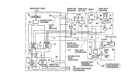
An instruction issue timing controller 29' (viz.,
the arrangement of Fig. 6), differs from the counterpart
29 (Fig. 3) in that the controller 29' further includes
an instruction ch~; ni ng controller 80 and a time slot
number register 82 which is provided in the entry number
coincidence determiner 32. The remaining portions of
Fig. 6 will not be referred to for the sake of brevity
since already referred to, except for the cases necessary
for the discussion of the instant invention. The
instruction ch~; n; ng controller 80 includes two flag
registers 84, 86, a counter 88, and a slot timing
detector 90.
According to the present invention, even if a RAM
CA 02087678 l998-Ol-l9
- 16 -
read instruction is to access the memory block which is
also designated by a preceding RAM write instruction, the
issue timing of the RAM read instruction can be generated
without waiting for completion of the preceding RAM write
instruction.
In other words,when the controller 29' receives a
RAM write instruction, the controller 29' sets a
predetermined time period for which a RAM read
instruction applied to the controller 29' at a later time
is prohibited to be issued if the two instructions use
same memory block. The predetermined time duration is
much shorter than the time period which is terminated
upon completing the RAM write instruction.
The present invention is not concerned with the case
lS where a RAM read operation is carried out on a memory
block which is different from that utilized in the
preceding RAM write instruction. In this instance, the
arrangement of Fig. 6 works in exactly the same manner as
described in connection with Fig. 4.
The operations of the Fig. 6 arrangement will be
discussed with reference to Fig. 7. For the purpose of a
better understanding, the same instructions as already
described in connection with Fig. 5 are again presented.
That is,
VADD VD0 ~ VR0 + VR1
VMDA VR2 ~ VD0
The instruction VADD is executed in exactly the same
manner as descri~ed in connection with Fig. 4 and
accordingly, the instructlon VADD will not be referred to
in detail. The following instruction VMDA includes a RAM
read operation on the same memory block VD0 as used by
the instruction VADD. The data retrieved from VD0 are
moved to the register VR2 (not shown).
The instructions VADD and VMDA are respectively
applied to the controller 29' at reference time slots T2
71024-222
CA 02087678 l998-Ol-l9
- 17 -
and T3, as illustrated in Fig. 7.
Thus, at reference time T3, the entry number
retainer 50 stores the entry number VD0 which is
accompanied by the instruction VADD. The flag register
44 still holds a flag bit assuming a logic 1 in that the
instruction VADD has not been completed. Therefore, the
output of the AND gate 62 (viz., coincidence signal D)
assumes a logic 1 at reference time T3.
Before the instruction VADD is applied to the
controller 29', the counter 88 receives a value
indicative of time duration defined by
PPT + FUT - SLT
where SLT denotes the number of time slots 0-3 (viz., 4
in this particular case) which equals the number of the
memory units MU0-MU3 (Fig. 1). Since PPT=3 and FUT=7,
PPT + FUT - SLT = 6. It is necessary to renew the
content of the reset circuit 88 if FUT is different from
the previous value.
When a control signal which indicates the issue
timing of the instruction VADD is generated at reference
time slot T2, the signal B is applied to the counter 88
and the flag registers 84, 86 at reference time slot T3.
The counter 88 is responsive to the signal B and starts
counting-up of the above mentioned time slots using
clocks applied thereto. On the other hand, each of the
flag registers 84, 86 changes the flag bit from "O" to
"1" in response to the signal ~ (viz., the registers 84,
86 are set). When the counter 88 has counted up six time
slots, it changes the content of the flag register 84
from "1" to "0" at reference time slot T9 (viz., the
register 84 is reset). Since the output of the flag
register 84 is inverted, the slot timing detector 90 is
supplied with a logic 1 from the flag register 84.
In response to the resetting of the flag register
84, the detector 90 initiates the operations thereof.
71024-222
CA 02087678 l998-Ol-l9
- 18 -
That is, the detector 90 receives a signal E from the
time slot number register 82. The signal E indicates
time slot 0 which is to be used by the instruction VADD.
Further, the slot timing detector 90 receives a signal F
which indicates the output of the time slot counter 66
(viz., time slots 0-3). When the time slot applied from
the register 82 (viz., "0") coincides with that applied
from the time slot counter 66, the detector 90 resets the
flag register 86 (viz., the content of the register 86
changes from "1" to "0"). The flag bit of the flag
register 86 is inverted and then applied to the read
instruction controller 47.
The read instruction controller 47 is already
informed of time slot 1 (viz., the time slot having the
smallest number among the available slots) which is to be
used with the instruction VMDA. The controller 47, in
response to the resetting of the register 86, detects the
timing of time slot 1 using the output of the read-out
time slot timing determiner 64 at reference time slot
T12. In Fig. 7, a line P indicates a time period for
which the issue of the RAM read instruction is prohibited
in the above mentioned embodiment.
Following this, the read instruction controller 47
generates a logic 1 which is applied to the indicators
54, 56 and 58. In this instance, the time slot indicator
56 stores time slot 1 which is used in the following RAM
read operation.
After three time slots of PPT (T13-T15), vector
elements stored in the memory block VD0 at reference time
slots T15-T22 are successively read out using time slot 1
at the following reference time slots T16-T23,
respectively. The vector elements thus retrieved are
succeedingly stored in the register VR2 at reference time
slots T19-T26 in this embodiment.
In the above discussion, the slot timing detector 90
71024-222
2087 67~ NE-466
detects the coincidence of the time slots applied from
the time slot number register 82 and the time slot
counter 66. However, the present invention is not
limited to such a case. As an alternative, the detector
90 may be arranged to reset the flag register 86 when
detecting the time slot number difference of the two
slots applied thereto which indicates one or two (for
example).
As mentioned in the opening paragraphs, two or more
entry number coincidence determiners may be provided
which are respectively assigned to the multiple paths to
the RAM 10 (Fig. 1). In such a case, it is necessary to
provide the same number of instruction chaining
controllers which are respectively assigned to the
multiple paths.
It will be understood that the above disclosure is
representative of two possible embodiments of the present
invention and that the concept on which the present
invention is based is not specifically limited thereto.