Note: Descriptions are shown in the official language in which they were submitted.
W092/02094 PCT/US91/05061
2~77~
DESCRIPTION
SAWC Phase-Detection Method and Apparatus
- Backaround Of The Invention
This invention relates to spread spectrum
communications, and more particularly to a spread spectrum
receiver that utilizes a phase coded surface-acoustic-wave
device or other analog device.
Description Of The Prior Art
A spread spectrum system is one in which the
signal energy is distributed over a frequency spectrum
that is much wider than the maximum bandwidth required to
transmit the information being sent. Techniques for
direct sequence spread spectrum modulation have been
developed for several years to promote among other
benefits, secure communications. Modulation is achieved
by mixing (or multiplying) the information to be sent wi~h
a periodic pseudo-noise (PN) code. The spectral density
function for the resulting signal has a sin(X~/X shape
with a very wide ~andwidth, as compared to the
information, and a lower spectral density functisn
amplitude as compared to the information. This
modification of the original spectral density function
reduces the signal's sensitivity to in-band interference
and jamming, as well as reducing interference to other
equipment that is sensitive to radio frequencies. Among
the other advantages inherent to a spread spectrum system
are selective addressing capabilities, code division
multiplexing for multiple access, and' highly accurate
ranging capabilities.
Due to the encoded nature of the signal,
demodulation is a more involved process compared with
demodulation schemes associated with traditional
communications systems. In this case, demodulation
involves a receiver reference code, identical to that
2~877~ 2
W092/02094 ~ PCT/US91/05061
transmitted, that synchronizes the receiver wi~h the
transmitter. The difficulty with this process is that
there is no indication of the degree of
non-synchronization between received and reference codes
until a very high degree of synchronization is achieved.
Additionally, mismatches between transmit and receive
oscillators used to generate PN codes tend to cause drift
in the synchronization between transmitter and receiver.
A prior art communications system using two
pseudo-random waveforms and two correlators for
designating a MARK and a SPACE, is disclosed in U.S.
Patent No. 4,247,942, to Hauer, issued January 27, 1981,
which is incorporated herein by reference. Hauer
discloses in a communication system, a first delay line
having multiple spaced taps for supplying successive input
pulses to the delay line. In response to each input
impulse, variously delayed pulses appear at the taps of
the delay line, which are used to generate pulses
representing a MARK or a SPACE. His disclosure includes
synchronous detectors, and means for supplying the
carrier-transmitted pulses to the detectors.
The prior art does not teach or suggest an
apparatus having or using a single tapped delay line
surface-acoustic-wave-correlator (SAWC) device for
decoding either of two spread spectrum chip sequences or
N tapped delay line SAWCs for decoding a multiple of N
spread spectrum chip sequences.
Ob~ects And Summary Of The Invention
An object of the invention is to provide an
apparatus for demodulating, using SAWCs, a spread spectrum
signal which uses different codes for different
information symbols.
Another object o~ the invention is to provide an
apparatus for acquiring a spread spectrum signal without
the requirement of a separate synchronous reference code.
W0~2/02094 2 0 ~ 7 ~ 1 ~ PCT/US91/05061
An additional object of the invention is to
provide an apparatus which will acquire a spread spectrum
signal on each data bit received at the rate the data are
tran~mitted with no time loss due to code synchronization,
- 5 and without use of any code synchronization preambles.
Another object of the invention is to demodulate
a first data symbol represented by a first phase shift on
a carrier signal and having a spread spectrum chip
sequence modulating the first phase-shift on the carrier
signal, and a second data symbol represented by a second
phase shift on the carrier signal and having the spread
spectrum chip sequence modulating the second phase shift
on the carrier signal, using a SWAC appropriately tapped
for the spread spectrum chip sequence and a phase
detection device.
A still further object of the invention is to
demodulate a plurality of data symbols represented by a
plurality of phase shifts on a carrier signal and having
a spread spectrum chip sequence modulating the plurality
of phase shifts on the carrier signal, respectively, using
a SWAC appropriately tapped for the spread spectrum chip
sequence and a phase detection device.
According to the present invention, as embodied
and broadly described herein, a phase coded surface
2S acoustic wave correlator (SAWC) based spread spectrum
receiver for use on a spread spectrum signal employing a
phase-shift modulated carrier signal is provided
comprising a SAWC and a phase detector. The SAWC has
appropriate transducer and tapped delay line structures
phased-matched to a chip sequence of the phase-shift
modulated carrier signal, at the carrier signal frequency
or an equivalent frequency, such as an intermediate
frequency (IF). The carrier signal of the spread spectrum
signal is phase modulated by a data-symbol sequence. The
data-symbol sequence is coherently modulated by a
repetitively generated chip sequence. The repetitively
generated chip sequence is known as the spreading sequence
W092/02094 ~ PCT/~S91/0~061 ~--
2~877~`~
for generating the spread spectrum signal. ~he
data-symbol sequence usually includes information to be
communicated by the spread spectrum signal. Preferably,
each data symbol is modulated by a complete sequence of
the repetitively generated chip sequence.
In response to a spread spectrum signal having
a carrier signal which is phase modulated by a chip
sequence matched to the tapped-delay line structures of
the SAWC, the SAWC outputs a post-SAWC-signal pulse at the
carrier signal frequency or the equivalent frequency. The
post-SAWC-signal pulse has a data phase which corresponds
to the data symbol of the data-symbol sequence which
modulated the carrier signal. The post-SAWC-signal pulse
has a signal-to-noise enhancement, which is also known as
processing gain, that is a function of the number of chips
in one complete chip sequence.
Additional objects and advantages of the
invention will be set forth in part in the description
which follows, and in part will be obvious from the
description, or may be learned by practice of the
invention. The objects and advantages of the invention
also may be realized and attained by means of the
instrumentalities and combinations particularly pointed
out in the appended claims.
Brief Description Of The Drawinas And PhotoaraDhs
The accompanying drawings, which are
incorporated in and constitute a part of the
specification, illustrate preferred embodiments of the
invention, and together with the description serve to
explain the principles of the invention.
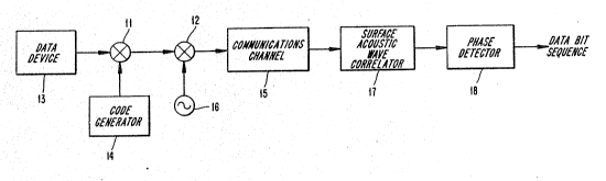
FIG. 1 illustrates one embodiment of a phase
coded surface acoustic wave device spread spectrum
receiver according to the present invention;
FIG. 2 shows modulo-2 addition for BPSK carrier
signal modulation, for a data-bit sequence and an eight
chip-code sequence;
W092/02094 2d877~2 PCT/~S9~/05061
FIG. 3A illustrates a post-SAWC-signal pulse for
an 80 nanosecond pulse;
FIG. 3B illustrates a time-expanded view of the
post-SAWC-signal pulse;
- 5 FIG. 4A illustrates a phase inverted version of
the post-SAWC-signal pulse; and
FIG. 4B is a time-expanded view of the phase
inverted post-SAWC-signal pulse.
Detailed Descri~tion Of The Preferred Embodiments
The invention disclosed in this patent is
related to the inventions disclosed in U.S. patent
application entitled "Spread Spectrum Correlator", by
Robert C. Dixon and Jeffrey S. Vanderpool and having
Serial No. 07t390,315 and Filing Date of August 7, 1989,
and in U.S. patent application entitled "Asymmetric Spread
Spectrum Correlator" by Robert C. Dixon and Jeffrey S.
Vanderpool and having Serial No. 07/389,914 and Filing
Date of August 7, 1989, which are expressly incorporated
herein by reference.
Reference will now be made in detail to the
present preferred embodiments of the invention, examples
of which are illustrated in the accompanying drawings.
The present invention includes the use of a SAWC
for demodulating a phase-coded spread spectrum signal. As
illustrated in FIG. 1, a spread spectrum transmitter and
receiver are shown including data-sequence-generating
means, chip-sequence-generating means, chip-sequence-
modulating means, carrier-modulating means, a SAWC device,
and phase-detecting means. The data-sequence-generating
means may be embodied as a data device 13 which outputs a
data-symbol sequence. The data-symbol sequence usually
includes information to be communicated by the spread
spectrum signal. The data-symbol sequence may have each
data symbol represent two or more data bits. In a binary
case, the data-symbol sequence has each data symbol
represent one data bit, and accordingly, the data-symbol
W092/02094 2a877~ 2 PCT/US91/05061 ~~
sequence is known as a data-bit sequence. As an example,
the data device 13 may be a computer terminal, a device
which has converted analog voice or video to data, or any
other source where data are to be transmitted from a
transmitter to a receiver.
The chip-sequence-generating means may be
embodied as a code generator 14 which repetitively
generates a chip seguence. The repetitively generated
chip sequence is known as the spreading sequence for
generating the spread spectrum signal. In a preferred
embodiment, the chip sequence is a pseudo-noise (PN) code.
The code generator 14 may employ shift registers having
appropriate taps for generating the chip sequence. The
chip sequence is generated coherently with each data
symbol, generated by the data device 13.
The chip-sequence-modulating means may be
embodied as a chip-modulating device ll. Preferably, each
data symbol is modulated by a complete sequence of the
repetitively generated chip sequence. For a binary case
~O where the data-s~mbol sequence is em~odied as a data-bit
sequence having l-bits and 0-bits, the chip-modulating
device ll can be realized with a modulo-2 adder, or an
exclusive-OR gate. Accordingly, the chip-modulating
device ll outputs the chip sequence from code generator
14 in response to a 0-bit from the data device 13, and an
inverted, 180 phase shifted, chip sequence in response to
a l-bit from the data device 13.
A signal source 16 generates a carrier signal.
The carrier-modulating means is coupled to the
chip-sequence-modulating me~ns and the signal source 16,
and may be embodied as a phase modulator 12. The phase
modulator 12 modulates the carrier with the output from
the chip-modulating device ll, causing phase shifts in the
carrier signal corresponding to each state transition of
the chip sequence. The spread spectrum signal is the
carrier signal, modulated with the output from the chip
modulating device ll. Thus, the carrier signal of the
W092/02094 PCT/US91/05061
2387~1 ~
spread spectrum signal is phase modulated by a
repetitively generated chip sequence, which is coherently
phase modulated by a data-symbol sequence. The phase
modulator 12 outputs the spread spectrum signal to a
communications channel 15.
By way of example, FIG. 2 illustrates the
operation for BPSK carrier signal modulation and modulo-2
addition for a data-symbol sequence embodied as a data-bit
sequence, and an eight chip code sequence. Shown are a
code chip clock, chip sequence, data-bit sequence, carrier
signal, and phase modulated carrier signal. The data-bit
sequence forces a 180~ code sequence phase shift for each
change in the data-bit sequence. The chip sequence in
turn causes a 180 carrier signal phase shift for each
change in the chip sequence.
A phase coded surface acoustic wave correlator
(SAWC) based spread spectrum receiver for demodulating the
spread spectrum signal having the phase-shift-modulated
carrier signal is provided comprising a SAWC 17 and
phase-detecting means. The SAWC 17 has appropriate
transducer and tapped delay line structures phased-matched
to the chip sequence of the phase-shift modulated carrier
signal, at the carrier signal frequency or an equivalent
frequency, such as an intermediate frequency (IF).
A SAWC is a passive device designed to recognize
a specific sequence of code chips and accomplishes this
through a correlation of phase shifts in an RF signal.
Each delay element within the SAWC device has a delay
equal to the period of the clock of the transmitted chip
code such that each element corresponds to only one chip
at any one time. As the received signal propagates down
the SAWC device, the phase structure of each element is
added in or out of phase with the propagated received
signal, and the outputs of all the elements from the SAWC
are summed in phase to arrive at a total correlation
value. When all the phase shift structures of the
W092/02094 2 0 8 7 7 ~. ~ PCT/US91/05061 -~
elements match the phase shifts of the received signal,
then the maximum sum and correlation is achieved.
In order to achieve the desired correlation, the
correct reference code must be "loaded" onto the SAWC
device. The present discussion is for a BPSK device,
however, the invention extends and includes any PSK
process such as MSK, QPSK, etc. Assuming a binary-phase
shift keyed signal, 180 phase shifts occur at each
one/zero transition of the chip sequence. Receiver
detection with a SAWC is usually accomplished in one of
two ways. The first is through a programmable SAWC which
allows progra~ming all phases in each element by a user.
The inverted and non-inverted phase elements are summed.
The second is through a non-programmable SAWC.
In non-pro~rammable SAWCs, the phase shifts are
programmed at the time of construction through transducers
placed in each element to produce an elemental phase
match. The non-programmable SAWCs cannot be changed by
the user. Thus, only one chip sequence can be correlated
The inverted and non-inverted phase elements of the coded
SAWC are then summed together just as in the progra~mable
device.
A received signal, which is phase-shift-key
modulated with a chip sequence at an RF frequency
equivalent to that in the SAWC, is amplified and fed to
the SAWC. The received signal may be down-converted,
although down conversion to an IF frequency is not
preferred unless necessary, before being fed to the SAWC.
As the received signal propagates across the surface of
the SAWC, the energy in each delay element increases by a
factor determined by the phase of the reference elements
versus the received signal phase. When the received
signal propagates to the end of the delay line correlator,
and all the phase shifts in the received signal match the
phase shifts in the SAWC, a maximum correlation energy is
attained. At this point, the SAWC outputs a
post-SAWC-signal pulse.
W092/02094 2 0 ~ 7 7 1~ 2 PCT/US91/~5061
The post-SAWC-signal pulse has a signal-to-
noise enhancement, which is also known as processing gain,
that is a function of the number of chips in one complete
chip sequence. The post-SAWC-signal pulse typically is a
two-chip-wide pulse which comprises the carrier signal
~odulated with the first phase or the second phase.
Essentially, the post-SAWC-signal pulse is a very narrow
pulse of the carrier signal phase modulated with the data
bit sequence.
Referring to FIG. 1, in response to a spread
spectrum signal having a phase-shifted modulated carrier
signal which is phase modulated by a chip sequence matched
to the tapped-delay line structures of the SAWC 17, the
SAWC 17 outputs a post-SAWC-signal pulse at the carrier
signal frequency or the equivalent frequency. The
post-SAWC-signal pulse has a data phase which corresponds
to the data symbol of the data-symbol sequence which
modulated the carrier signal.
The phase detecting means may be embodied as a
phase detector 18. The phase detector 18 is coupled to
the surface-acoustic-wave correlator 17. The phase
detector 18 detects the changes in phase in the
post-SAWC-signal pulse outputted from the
surface-acoustic-wave correlator 17. In response to
detecting a particular phase, the phase detector 18
outputs a corresponding data-symbol.
The phase-detecting means may, for example, be
embodied as a phase detector 18 which compares the phase
of adjacent bits in the carrier signal outputted from the
surface-acoustic-wave device 17. This modulation is
commonly known as differential phase shift keying (DPSK).
Alternatively, the phase-detecting means may be
embodied in other ways, such as a phase-loc~ed-loop (PLL)
device which is coupled to the surface-acoustic-wave
device 17. The PLL device locks the phase and frequency
of a PLL signal onto the post-SAWC-signal pulse. A phase
comparator may be added to the output of the
W092/02094 2 0 8 ~ 7 ~ 2 PCT/US91/05061
phase-locked-loop device for comparing the phase of the
PLL signal with the phase of the post-SAWC-signal pulse
and thereby generate the data-symbol sequence.
An advantage of the present invention is the
ability to detect multiple data symbols from a single chip
sequence, phase modulated carrier signal by detecting the
phase of a very narrow post-SAWC-signal pulse outputted
from a SAWC. A transmitter can send, for example, a
carrier signal having phase shifts representing a
data-symbol se~uence using only one chip code. For the
binary case, the data symbols represented as data bits
determine whether to send a first chip code or a phase
shifted version of the first chip code. The present
invention requires only a single tapped delay line SAWC
for a matched filter, which is phase matched to the chip
code. For the binary case, the carrier signal is binary
phase shift key (BPSK) modulated with a chip sequence, and
the phase of the carrier signal can be shifted 180 at
every state transition of the chip sequence. For the
binary case, the chip sequence is further phase modulated
by a data-bit sequence whereby a first data-bit, i.e. a
1-bit, causes the chip sequence to be generated and a
second data-bit, i.e. a 0-bit, causes a 180 phase shifted
version of the chip seguence to be generated. Thus, the
carrier signal is phase shifted 180 at every state
transition of the chip sequence, and also phase shifted at
every state transition of the first and second data bits.
FIG. 3A illustrates a post-SAWC-signal pulse
having a first phase for an 80 nanosecond pulse outputted
from the surface-acoustic-wave correlator. FIG. 3B is a
time expanded view of the post-SAWC-signal pulse. FIG. 4A
illustrates a post-SAWC-signal pulse haYing a second phase
where the second phase is a 180 phase shifted version of
the first phase. FIG. 4B is a time expanded view of the
post-SAWC-signal pulse having the second phase.
The present invention may be extended to phase
shift keyed systems other than binary. By way of example,
wo 92/020g4 2 0 8 7 7 ~ 2 PCT/US91/05061
in a QPSK system, a single quadrature phase tapped delay
line SAWC would detect one of four phases by having a
carrier signal modulated in 90 phase shifts by one or
more chip sequences, as opposed to the two phases detected
in the BPSK system by a bi-phase tapped delay line SAWC.
In a QPS~ system, each chip sequence would represent one
of four data symbols, or two binary data bits.
The present invention may be extended to a ~-ary
system using the same underlying techniques as presented
herein. For example, a quaternary BPSK system would
utilize two chip codes to generate a first chip sequence
and a second chip sequence, and a 180 phase shifted
version of each chip sequence requiring only two tapped
delay line SAWC's. In this case, two chip sequences may
represent two of four data-symbols each, or two binary
bits. Two data-symbols would be represented by the first
chip sequence and a 180 phase shifted version of the
first chip sequence, respectively. Two additional
data-symbols would be represented by a second chip
sequence and a 180 phase shifted version of the second
chip sequence, respectively. Accordingly, a receiver
would require only two bi-phase tapped delay line SAWC's
to demodulate four symbols by phase comparing the
post-SAWC-signal pulses. This concept may be extended to
QPSK, etc.
This system may also be extended by using a
single chip sequence to represent more than two chip
sequence states. For example, in a BPSK system, the chip
sequence may represent a first data symbol, a phase
shifted version of the chip sequence may represent a
second data symbol, a time reversed, or "reciprocal"
version of the chip sequence may represent a third data
symbol, and a reciprocal, phase shifted version of the
chip sequence may represent a fourth data symbol.
More broadly, the present invention may include
N phase coded SAWC devices in a spread spectrum receiver
for use on spread spectrum signals including a carrier
W092/02094 2 0 8 7 7 ~ ~ PCTtUS91/05061 ^
signal phase modulated by a data-symbol sequence and one
of N chip sequences or phase shifted versions of the N
chip sequences. The chip sequences repetitively and
coherently are generated with the data-symbol sequence
- 5 determining the generation of one of the N chip sequences
or a phase shifted version of that chip sequence. A
plurality of N SAWC's are employed with each SAWC matched
to one of the N sequences. In response to the carrier
signal modulated with one of the data-symbol sequences and
chip sequences, the SAWC phase matched to the chip
sequence transmitted outputs a post-SAWC-signal pulse
whose phase is determined by the phase shift of the chip
sequence. In response to the post-SAWC-signal pulse, the
phase detection means, coupled to the SAWC output, detects
the phase of the post-SAWC-signal pulse and generates a
corresponding the data-symbol.
The present invention may be extended to M-ary
and/or MSK, or QPSK symbols using the same underlying
techniques as presented herein, where each phase shift
generated by a data sequence may represent a data symbol
or symbols. A single spread spectrum receiver may employ
one or more SAWC's, and a single SAWC may employ more than
one tapped delay line. A single SAWC device may have one
or more correlators, and a system may have one or more
SAWC's.
A difference between the method and apparatus of
this invention and those used in the prior art is that the
correlation pulse is used to directly derive the data
symbols, while other systems may use the pulse for
synchronizing a much longer reference code signal to the
incoming received code signal.
A difference between SAWC devices and digital
correlators is in the frequency bands in which they are
used. The SAWC devices are usually employed at IF, but
they can be used at RF. The digital correlators are
usually used at baseband. Another difference is that SAWC
devices perform phase shift comparisons while the digital
W092/02094 ~ PCT/US91/~06l
2087712
correlators perform voltage level comparisons. Further,
the SAWC devices sum the outputs differently from that of
digital correlators. Also, when the present invention is
realized with a SAWC correlator, no receive code clock is
required to correlate the PN code. The present invention,
using a SAWC correlator, may be realized using fewer
components.
It will be apparent to those skilled in the art
that various modifications can be made to the phase coded
spread spectrum SAWC receiver for decoding a received
spread spectrum signal, which includes a data signal
modulated with a PN code, of the instant invention without
departing from the scope or spirit of the invention, and
it is intended that the present invention cover
modifications and variations of the phase coded spread
spectrum SAWC receiver provided they come within the SCOp2
of the appended claims and their equivalents.