Note: Descriptions are shown in the official language in which they were submitted.
20s7~$~
A SYSTEM FOR DISTRIBUTED POWER MANAGEMENT
IN PORTABLE COMPUTERS
DESCRIPTION
Technical Field
This invention relates generally to computers. More
specifically, this invention relates to the management of
power in portable computers.
Background Art
Reducing power consumption in portable computers has gained
a great deal of attention in the technical community as a
result of a set of conflicting user requirements and
technological constraints. On the one hand, users would
like to operate these portable machines for extended periods
of time without access to ac power. This means that such
machines must carry their own power sources, i.e., batteries
of various types. On the other hand, the total energy
stored in such batteries varies almost directly in
proportion to their weight. Carrying heavy batteries of
course, detracts from the portakility attributes of these
machlnes.
Therefore, efforts in the industry have focused in several
related areas. First, designing components that consume
less power than corresponding components in desktop
ac-powered machines; second, detecting when such components
are not in use and turning them off or placing them in a
lower power consuming mode(s), thus reducing their energy
consumption over time; third, using batteries that provide
higher energy-to-weight ratios; and last, monitoring the
battery and providing the user alerts and related actions
due to the non-linear nature of battery power output as a
function of time.
YO9-91-151 2 2087767
The power management techniques which are currently practiced in the personal computer industry
commonly address a combination of one or more of these areas. World PCT App. No. 91/00566
to Harper et al., published January 10, 1991, describes the design elements of the POQET
C~ JUl~I. The POQET C(~ ]U~;I has been designed with several low power components such as
low power display element, low power Universal Asynchronous Receive Transmit (UART)
component, etc. Additionally, circuitry has been designed that detect the occurrence of certain key
events in the system such as the occurrence of a key press on the keyboard, system timer signal,
access to a special memory location commonly known as the interrupt vector, etc. The occurrence
of any of these events triggers a Non-Maskable Ill~ellupt (NMI) to the processor which then
executes a special block of power management code. This code then determines if a change in the
power state of the system is warranted. There are several drawbacks to this approach. The scheme
of monitoring processor access to certain i~lt~llUpt vector locations and thereby deducing that the
operating system and/or applications are idle, don't apply to advanced processors such as the Intel
80286/386 operating in the so-called protected mode of operation. In these processors, the location
of the inl~.~ u~ vectors is not fixed. As a result, the address lines external to the Central Processing
Unit (CPU) cannot be monitored to determine if a particular i~ltellupl is vectored to a particular
location. Nor can they be relied upon to work correctly in multi-tasking environments such OS/2
or the more recent Penpoint operating system developed by GO. Corp. for pen-based colllpu~
Such operating systems generally do not issue software inlellupts to indicate an idle state.
Furthermore, in the advanced processors cited above, the interrupt vectors themselves are not
guaranteed to be in any given memory address. Thus, while the POQET design works well with
real mode DOS applications, it is inadequate for environments using multi-tasking operating
systems executing on processors such as 386.
U.S Pat. No. 5,041,964 to Cole et al. describes the power management hardware and software of
a GRID laptop computer.
YO9-91-151 3
~2o87~6~l
In this computer, a standby mode is defined in which power
to most parts of the computer except dynamic memory is
removed when one of a set of pre-defined events occurs.
Power is restored to the system when the user so indicates
(by a push button) and there is sufficient battery power to
enable proper system functioning. As in the case of the
POQET computer, the solutions in this patent break down in a
multitasking environment where multiple applications may be
active at once and in advanced microprocessors such as the
Intel 80386 and compatibles wherein the operating system can
(and does) disable NMI interrupts from occurring or
re-vectors them to code fragments that may have no knowledge
of the nature of NMI being presented to the computer.
In the European Patent Application No. 90311832.1, Watts and
Wallace describe an apparatus and a method whereby the CPU
clock is reduced whenever a real-time monitor determines
that CPU activity level is low. The reduced clock rate
results in lower power consumption by the CPU. Such
apparatus has been incorporated in highly integrated chip
sets available from several chip vendors. However, Watts
does not teach how to apply such techniques when multiple
CPUs are involved in the operation of a computer. In fact,
applying the above methods to a single microprocessor,
albeit the main processor, without overt coordination among
the principal points of intelligence within the system may
result in a net increase in power consumption.
International Pat. Appln. No. PCT/US89/05576 to Bolan et
al., a method whereby the power consumed by a certain
microprocessor can be controlled externally by a chip. This
chip is designed to consume very low power. As in the
previous teachings, such methods and apparatus are readily
available from a number of chip vendors. What is missing
from the Bolan device is a description of how these
mechanisms can be applied to the design of a distributed
power managed computing platform such as a pen based tablet
computer.
YO9-91-151 4
208~767
Other implementations, including the IBM laptop computer
(the PS/2 L40SX computer), have provided for user
specifiable time-outs for various power consuming devices.
When no input/output (I/O) activity is perceived for a
time-out period on a given component, that component is
placed in a low power state. For example, many
implementations include a specifiable time out value for the
hard file. At the end of the time out period, if no
activity has occurred, the device is turned off. However,
it must be noted that extra power is expended when the hard
file is turned on again and furthermore, the CPU has to wait
(wasting energy) while the spin-up is taking place. Studies
have shown that no single time out value is likely to result
in optimal power conservation. Thus, it is difficult if not
impossible for users in general to provide appropriate
timeout values for devices in a portable system.
What is needed is a power management system which can
operate effectively in multi-tasking, multiple-CPU systems
and advanced processors at a reduced rate.
Disclosure of the Invention
The present invention provides a system and method for
managing power in a portable, petl-based notebook computer.
The system and method provides a means for minimizing power
consumption by collecting and in~erpreting power related
data at various processing elements while hiding many of the
details from the end-user.
Power management is carried out co-operatively at several
layers. These layers include a system planar hardware
level, battery controller level, service processor level,
main processor firmware level, and operating system level.
At the system planar level, mechanisms for low power
operations are implemented. These mechanisms include
partitioning of peripherals and I/O devices into power
planes that can be independently turned on and off,
providing software switches that control power to these
planes and selection of devices that are capable of low
Y09-91-151 5
208~67
power standby modes of operation. In the battery controller
level, mechanisms are provided to turn power to the system
on and off and to collect data relating to the state of the
battery to send this information to the main processor. The
battery controller is a]sc responsible for protecting the
battery from excessive drain or operation under low charge
conditions. At the service processor level, circuits are
provided to monitor the on/off button and to communicate
power management events and battery state information to the
main processor on the system planar. The system firmware
and operating system software levels execute on the main
processor on the system planar and are responsible for
policy decisions such as when power planes can be shut down
and what to do when a power event takes place.
Features and Advantages
It is an advantage of the present invention to distribute
the power management function among three processors,
thereby reducing the amount of processing time the main CPU
is required to dedicate to -the power management function.
It is a further advantage of the present invention not
having to monitor address patterns to obtain access to
certain interrupt vector locations. This enables the
present invention to operate in advanced processors which
have a protected mode of operation and do not follow
conventional addressing standards.
It is a further advantage of the present invention to have
multiple processors operating asynchronously enabling one
processor to enter a low power mode of operation independent
of the other processors.
It is a further advantage of the present invention to have
an established communiclt~on protocol to transfer power
management data between multiple processors enabling each to
efficiently determine which power management functions to
perform by taking the states of the other processors into
consideration.
Y09-91-151 6
208~7~7
It is a further advantage of the present invention to
separate the computer into independently controlled power
planes enabling it to selectively power only those parts of
the computer necessary to perform the present functions and
without affecting the overall usability of the system.
It is a further advantage of the present invention to
immediately enter a low power mode of operation whenever
there are no instructions to perform.
It is a further advantage of the present invention to have a
zero power state wherein the computer enters such state only
after storing all application data. Having a zero power
state rather than an off state enables the user to turn off
the machine in the middle of running an application program
without losing data. The computer will save all the
necessary application data and return the computer to the
same state upon turning the system on.
It is a further advantage of the present invention to have
the capability to save CPU state and application data in a
secondary storage medium whenever battery power is low.
This reduces the need for a backup battery and thereby
reduces the weight of the computer
The foregoing and other objects, features and advantages of
the invention will be apparent from the following more
particular description of '~he preferred embodiments of the
invention, as illustrated in the accompanying drawings.
Brief Description of Drawings
FIGURE 1 is an illustration of the layering of the power
management elements of the present invention;
FIGURE 2 is a block diagram of the System Planar Hardware
Layer; FIGURES 3(a) and 3(b) are block diagrams of the Core
Chip Set Register Files;
Y09-91-151 7
87 r~ ~7
FIGURES 4(a) and 4(b) is a schematic block diagram of the
On/Off switch logic;
FIGURE 5 is a state diagram of the main processor and system
planar;
FIGURE 6 is a flowchart of the main processor firmware logic
for the Power Management Interrupt Handler;
FIGURE 7 is a flowchart of the main processor firmware logic
for transitioning between the full power state and the low
power state;
FIGURE 8(a) is a flowchart of the main processor firmware
logic for entering the zero power state from the full power
state;
FIGURE 8(b) is a flowchart of the main processor firmware
logic for entering the zero power state from the full power
state;
FIGURE 9(a) is a flowchart of the main processor firmware
logic for entering the standby power state from the full
power state;
FIGURE 9(b) is a flowchart of the main processor firmware
logic for managing the RESUME PM event and entering the full
power state from the standby power state;
FIGURE 10 is an interface block diagram illustrating the
service processor interface signals;
FIGURE 11 is a state diagram of the service processor
flrmware;
FIGURE 12 is a flowchar~ of the service processor main loop
processing; FIGURE 13 is a block diagram of the battery
controller;
YO9-91-151 2087767
FIGURE 14 is a block diagram for the start up circuitry and low power linear regulators of the
battery controller;
FIGURE 15 is a block diagram of the battery controller power converter assembly;
FIGURE 16 is a block diagram for the power control logic of the battery controller;
FIGURE 17 is a block diagram for the battery monitor of the battery controller;
FIGURE 18 is a flowchart of the main loop executed by the battery controller fi~lllwale;
FIGURE 19 is the data tr~n.cmi.csion protocol between the battery controller and the service
processor;
FIGURE 20 is a state diagram of the battery microcontroller;
FIGURE 21 is a flowchart of the on/off button logic.
Best Mode for Carrying Out the Invention
The preferred embodiment of the present invention for use in a portable, pen-based notebook
com~uler is disclosed herein. In the ple~lled embodiment, the computer is logically compatible
with an IBM(E~ Personal Computer/AT(~ standard computer and has an Intel 386SX or an AMD
AM386SXL main processor. It is equipped with an integrated LCD panel and fligiti~çr and
packaged to resemble a notebook with a writing surface.
The power management function is carried out co-operatively at several levels or layers as
illustrated in FIGURE 1. The most external layer, the applications layer 112, represents any
software which is installed by the user and executed on the notebook computer. The functional
layers of the power management system are contained within this broader applications processing
layer 112. Specifically, there are five functional levels:
(1) System Planar 102
~'
Y09-91-151 9
20~7 ~ ~ ~
(2) Battery Controller 104
(3) Service Processor 106
(4) Main Processor Firmware 108
(5) Operating System 110
These five functional levels work in conjunction to maintain
the computer in one of four operational states. The present
state (full power or normal, low power or idle, standby or
sleep , or zero power) of the system determines what
functions are performed at each of the five layers.
These four states are briefly described with reference to
FIGURE 5. Each state and transition shall be fully
described in section II. The full power or normal state is
the fully operational and active state. As shown in FIGURE
5, every change in state must involve the normal state. In
the low power or idle state the system is operational but
only necessary functions are being powered. The computer
appears to be ON in this state. In the standby or sleep
state, the system appears to be OFF to the user, however,
there are certain system components which are powered and
the system will immediately resume its normal operation if
requested to do so. If not, the system will automatically
transition to the zero power state after a given period of
time. This is the lowest power state and the computer
appears to be OFF.
A brief description of the functlons performed at each of
these levels is given below.
At the System Planar Level 102, mechanisms for low power
operations are implemented. These mechanisms include
partitioning of peripherals and I/O devices into power
planes that can be independently turned on and off,
providing software switches that control power to these
planes, and selecting devices that are capable of low power
standby modes of operation. An example of this methodology
is the selection of a Solid State File (SSF) as the storage
media. The SSF consumes significantly less power while in
operation (active read/write) than comparable conventional
Y09-91-151 10 20877~ ~
rotating magnetic media files. It also consumes lower power
in non-operational modes such as the standby or sleep mode.
At the Battery Controller l,evel 104, mechanisms are
implemented to control the system power, collect status data
on the state of the battery, and transmit this information
to the main processor. Also, functions which are
responsible for protecting the battery from excessive drain
or operation under low charge conditions operate at the
Battery Controller Level 104.
At the Service Processor Level 106, circuits are provided to
monitor the on/off button and to communicate power
management events and battery state information to the main
processor on the system planar level 102.
The System Firmware Level 108 and the Operating System Level
110 contain software which executes on the main processor
which is part of the system planar level 102 and are
responsible for policy decisions such as when power planes
can be shut down and what to do when a power event takes
place.
The structure and operation of the preferred embodiment of
the present invention will be described in terms of these
layers.
I SYSTEM PLANAR LAYER
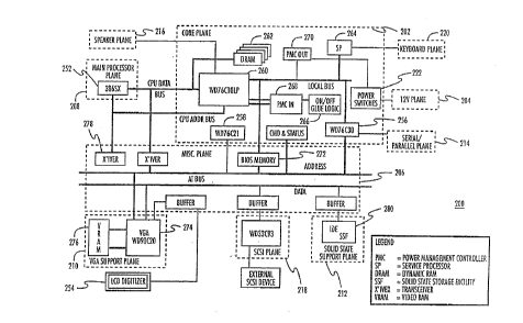
FIGURE 2 is a block diagram of the system planar level 200.
In the preferred embodiment, the system planar level 200 is
divided into ten power planes for the purposes of managing
power consumption. They are:
(1) Core Plane 202
(2) 12 Volt Plane 204
(3) Miscellaneous Plane 206
(4) Main Processor Plane 208
(5) VGA Support Plane 210
(6) Solid State Support Plane 212
Y09-91-151 11
208~
(7) Serial/Parallel Plane 214
(8) Speaker Plane 216
(9) SCSI Plane 218
(10) Keyboard Plane 220
A brief description of each power plane and the conditions
under which it receives power is given below with reference
to FIGURE 2.
1. Core Plane 202
The core plane 202 is comprised of three vendor chips 256,
258 and 260 (described in detail below) which enables the
invention to be compatible with an IBM Personal Computer AT.
These chips comprise what is defined as the core chip set
and perform many power control functions. Core Plane 202 is
also comprised of power switching circuitry 222, up to 16M
of dynamic RAM (DRAM) memory 262, a service processor 264,
power management control logic (PMCIN 268 and PMCOUT 270),
and on/off button glue logic 266. The core plane 202
remains powered during all power states of the system except
the off state. Removal of power from this plane cannot be
accomplished directly by the main processor 252. Instead,
the main processor 252 requests the battery controller (not
shown), via service processor 264, to remove power to the
entire system planar 200.
2. 12 Volt Plane 204
The 12 volt plane 204 carries a specific voltage (i.e., 12
volts) used in support of power switch circuits 222 located
the core plane 202. These circuits 222 control power to all
the power planes except the core plane 202, 12 volt plane
204, and to the miscellaneous plane 206. Furthermore, it is
possible for the firmware in the main processor to actuate
these power switch circuits by programming certain registers
located in the core plane 202. These will be fully described
below. The 12 volt plane is powered as long as the core
plane is powered. Similar to the core plane 202 the 12 volt
plane 204 is not directly controllable by the main processor
firmware or operating system software.
Y09-91-151 ~2 20~767
3. Miscellaneous Plane 206
The Miscellaneous Plane 206 includes the AT address and data
bus transceivers 278, and the BIOS memory 272. The BIOS
memory 272 contains the firmware needed to support multiple
operating systems and certain power management functions.
The Miscellaneous plane 206 receives power only in the full
power state and the low power (idle) state of the system.
4. Main Processor Plane 208
The Main Processor plane 208 powers the Intel 386SX (or
AM386SXL) processor chip 252. This plane is powered down by
the core chip set (256, 258, 260) whenever the system enters
the standby (sleep) state or the zero power state.
5. VGA Support Plane 210
The VGA Support plane 210 includes a VGA controller 274 with
LCD control and display memory VRAM 276. The VGA controller
274 is a low-power vendor chip WD9OC20. It provides the
driver for an LCD flat panel which is industry standard VGA
compatible. This plane remains powered in all states except
the zero power state of the system. However, the VGA
controller 274 itself is placed ill a low powered mode when
the system enters the standby state. In this mode, the
display memory 276 is slow-refreshed to preserve the
contents of the screen, although the screen (i.e., the LCD
panel and backlight both not shown) has been powered down.
This scheme allows the system to restore the visual state of
the screen without reloadinq the display memory 276 when the
system enters the full power state from the standby state.
6. Solid State Support Plane 212
The Solid State Support Plane 212 powers the solid state
file (SSF). It is powered down when the system enters the
standby state or the zero power state. It receives power
when the system is in the full power state and in the idle
state.
7. Serial/Parallel Plane 214
The Serial/Parallel Plane 214 supplies power to the serial
and parallel port control logic portion of the WD76C30 chip
Y09-91-151 13 20~7~67
256. This part of the chip, which is located in the core
plane 202, is separately powered from the remaining parts of
the chip. The Serial/Para!lel Plane 214 receives power in
the full power state or in the idle if and when an
application re~uests the use of the underlying devices (not
shown). It is turned off by the operating system after the
said application has indicated that it no longer needs use
of the devices.
8. Speaker Plane 216
The Speaker Plane 216 includes the audio amplifier of the
system speaker. This plane receives power in the full power
state only if and when an application requests use of the
speaker. It is turned off by the operating system after the
application has indicated that it no longer needs the use of
the speaker.
9. Small Computer System Interface (SCSI) Plane 218
The SCSI Plane 218 provides power to the SCSI controller and
associated logic. This plane receives power in the full
power state only if and when an application requests use of
a device (not shown) attached to the SCSI plane. It is
turned off by the operating system after the application has
indicated that it no longer needs use of the attached
device.
10. Keyboard Plane 220
The Keyboard Plane 220 controls power to an (optional)
keyboard. This plane is powered in the full powered state
and in the idle state of the system. It is powered down in
the standby state and in the zero power state.
Core Plane Detailed Description
The core plane 202 is ccmprised of the core chip set 256,
258, 260 which performs numerous power control functions.
The core plane 202 is alc,o comprised of the on/off glue
logic 266 which monitors the condition of such systems as
the battery and on/off switch to determine if an event has
occurred which may require the state of the system to
change. An event of this nature is defined as a power
Y09-91-151 14 2~87~6~
management (PM) event. The core chip set and the glue logic
portions of the core plane 202 perform critical functions in
the power management system, and are described below.
Core Chip Set Description
The compatibility with an IBM Personal Computer AT and many
power control functions are accomplished by what is defined
as the core chip set. The three vendor chips 256, 258, 260
which comprise the core chip are fully described in "Western
Digital 1991 Devices Databook," Western Digital Corp., l991.
The core chip set is comprised of registers which are
programmed to control the ten power planes of system planar
200. Each of the chips of the core chip set have been
specifically designed for low power consumption. The vendor
chips are described below, followed by a description of the
register files contained therein.
1. WD76ClOLP 260
This CPU and core logic controller chip incorporates a
memory controller, main processor control, AT bus logic
including DMA signals and power management control. Power
management control implements a register file that can be
accessed from the main processor and that allows for
altering the clock speed of the main processor, for shutting
down the main processor and/or other power planes in the
system and for resuming the execution of the main processor
upon the occurrence of one or more external events.
2. WD76C21 258
This chip implements a floppy disk controller, real-time
clock and IDE hard file control signals.
3. WD76C30 256
This chip implements standard AT style serial and parallel
ports, programmable interrupt controllers and clock
generators.
Core Chip Set Register Files
In the preferred embodiment, access to all power control
functions and related data is achieved through a set of I/O
Y09-91-151 15
208 7 7 S ~
buffers defined as register files. These register files are
implemented in the core plane and illustrated in FIGURES
3(a) and 3(b). The following is a description of each of
these registers and their associated functions:
1. Power Down Control Register (PDCR) 302
Two bits in the PDCR register 302 are of interest to power
management. The first bit controls the power to the main
processor plane 208. The other bit controls when there is a
full power down sequerlce. This sequence will turn off the
miscellaneous plane 206, the main processor plane 208, and
optionally the VGA support plane 210.
2. CPU Clock Control Register (CCCR) 304
The CCCR register 304 contains the main processor clock
speed. The CCCR register 304 may be programmed to reduce
the main processor clock to 1/2, 1/4th or 1/8th its normal
value. Since the power .-onsumption of a processor is
proportional to the clock speed, operating the main
processor 252 at the lowest possible clock speed will result
in the maximum power saving.
3. Refresh Control Register (RCR) 306
The RCR register 306 contains the refresh rate of the system
random access memory (RAM). It can be programmed to reduce
the refresh rate to ]/8th the normal value whenever the
system planar 200 enters the standby state.
4. Power Plane Control Register (PPCR) 308
The PPCR register 308 contains one bit for controlling power
to each of the following power planes: speaker plane 216,
VGA support plane 210, solid state support plane 212, SCSI
plane 218, Serial/Paralle] plane 214, and keyboard plane
220.
5. Screen Timer Control Registers (STCRs) 310,312
Power to the LCD panel and its backlight are controlled by a
pair of STCR timer registexs 310, 312. The STCRs 310 and 312
can be set up to control the amount of time for which the
Y09-91-151 ~6 208776~
LCD and backlight will be powered when there is no activity
on the system.
6. Power Management Interrupt Mask Register (PMIMR) 314
The PMIMR register 314 is comprised of three mask bits
corresponding to three power management (PM) events. A PM
event is a condition change which may require the system to
change state. Setting a bit to a 1 enables the corresponding
PM event to raise a power management (PM) interrupt to the
main processor 252. Settjnc~ the bit to a zero will prevent
the PM event from causing a PM interrupt.
7. Power Management Interrupt Status Register (PMISR) 316
The PMISR register 316 contains the PM events which have
caused a PM interrupt. This register is interrogated by the
main processor 252 to determine which of the three PM events
caused the latest PM interrupt.
8. Power Management Event Register (PMEVR) 318
The PMEVR register 318 contains information as to which PM
event(s) took place. This register records the event and
maintains a limited historical file of which events have
occurred.
On/Off Glue Logic Description
FIGURE 4 is a schematic block diagram of the on/off glue
logic 266 contained in the core plane 202. On/off glue
logic 266 monitors the condition of such systems as the
battery and on/off button to determine if an event has
occurred which may require attention by the system. These
inputs are received on the following input signal lines:
1. LOW BATT
The on/off glue logic 266 receives the low battery condition
signal on the LOW BATT signal line 402 from the service
processor 264. This signal indicates that the battery
charge is low enough to aLert the system.
2. TIMER INT
YO9-91-151 20877 67
The on/off glue logic 266 also receives a timer interrupt
signal on the TIMER INT signal line 404 from the real-time
clock 432 which represents when a time-out condition has
occurred. For example, if the system is in a normal power
state and no activity has occurred for a predetermined
length of time, the real-time clock 432 will transmit a
timer interrupt signal to notify the system of the lack of
activity.
3. RI
The on/off glue logic 266 also receives notification of an
external modem call on the ring indicator (RI) signal line
406 from the modem interface 434.
4. RESCLR
The on/off glue logic 266 also receives a resume clear
command on the RESCLR signal line 408 from the service
processor. This signal commands the on/off glue logic 266
to delatch the on/off button.
5. ON/OFF
The on/off glue logic 266 also receives an indication of
when the on/off button 438 has been pressed on the ON/OFF
signal line 410.
6. FULLPDN
The on/off glue logic 266 also receives a full power down
signal on the FULLPDN signal line 412 from the PMCOUT
register 270. This signal indicates when the system is in
the standby state.
The on/off glue logic 266 processes these inputs and
generates appropriate output signals representing certain
events which need to be addressed by the power management
system. The three output signal lines are the RESUME signal
line 426, SUSPEND signal line 422, and SPIRQ signal line
424.
1. RESUME signal line 426
Y09-91-151 1~ 2087767
The on/off glue logic 266 generates the RESUME signal on the
RESUME signal line 426 when the system planar 200 is in the
standby state (FULLPDN signal line 422 is active) and the
on/off switch 438 has been pressed, the real-time clock 432
generates a timer interrupt signal, or there is a modem call
ring indication. The RESUME signal will be inhibited if the
on/off glue logic receives a low battery signal on the LOW
BATT signal line 402 from the service processor 264.
2. SUSPEND signal 1ine 422
The on/off glue logic 266 generates the SUSPEND signal on
the SUSPEND signa] line 422 when a low battery signal 402 is
received from the service processor 264.
3. SPIR~ signal 424
The on/off glue logic 266 generates the SPIRQ signal on the
SPIRQ signal line 424 when the on/off signal line 410
indicates that the on/off button 438 has been pressed when
the FULLPDN signal line 412 indicates that the system was
not in standby (normal or low power states). The SPIRQ
signal is also generated when the low battery power
condition signal is received on the LOW BATT signal line 402
and there is either a timer interrupt, modem call, or the
on/off button is pressed, as described above for the RESUME
signal line 426 output.
Power Management Events
There are three types of power management events that are
recognized by the system planar's core chip set. These PM
events are:
1. Suspend PM Event
A SUSPEND PM event i 5 detected whenever the service
processor 264 determines that the charge of the battery is
below a particular threshold. The processing of the low
battery signal is performed by the on/off glue logic 266 and
presented on the SUSPEND signal line 422 as discussed above.
The vendor chip 260 will generate a SUSPEND PM event based
on the state of this output signal and the state of the
system. A SUSPEND PM event will only occur when the system
Y09-91-151 19
2~87767
is in the full power (normal) or low power (idle) state. A
low battery condition in the standby state will not generate
a SUSPEND PM event; rather, it will prevent the system from
returning to normal power and wi]l eventually turn itself
off.
2. Resume PM Event
A RESUME PM event is detected whenever the system is
requested to return from the standby state to address either
a timer interrupt, modem call, or user demand. This is
determined by the state of the on/off glue logic 266 RESUME
output signal 426 and the state of the system. The system
will only "resume" operation from the standby state; it is
not operational in the normal and idle states.
3. PCUINT PM Event
This is an event that may be generated by the service
processor 264 and detected by the core chip set whenever the
system planar level 200 is in the full power (normal) state.
This is one of many interrupts that may occur in the system
and will occur due to many conditions, including when the
on/off glue logic 266 generates a SPIRQ output signal. All
PM events are recorded in the power management interrupt
status register (PMISR) 316 and the power management event
register (PMEVR) 318 implemented in the core chip set 256,
258, 260 and accessible by the main processor 252.
Additionally, the main processor 252 can specify which of
these events will generate a PM lnterrupt by setting the
appropriate bits in the power management interrupt mask
register (PMIMR) 314. In the preferred embodiment, the PM
interrupt which is generated as a result of the PM events
described has been designated as IRQ level 11 (IRQ11).
PM Event Reason Codes
As seen above, the PM events are generated upon the
occurrence of different conditions and the state of the
system. The different callses which generate the PM events
are represented in the system hy what has been defined as a
reason code. The reason code is used by the system to
determine how to respond to a particular PM event. The
YO9-91-151 20
20~7 i6 ~
reason code will indicate one or more of the following
conditions:
1. Battery Warning
This indicates that the battery charge is low enough to
warrant a suspension of computer operation. This
condition will cause a SUSPEND PM event if the system
is in the full or idle state. If the system is in the
standby state the service processor 264 will re~uest
the battery controller to turn the system power off.
This results in the system entering the zero power
state.
2. On/Off Button Pressed
This indicates that the user has pressed the on/off
button 438. This condition will cause a PCUINT or
RESUME PM event.
3. External Source Present
This indicates if an external DC source is present and
that the system i 9 no longer dependent on battery
power. This condition will c~use a PCUINT PM event.
4. Excessive Battery/Ambi~nt Temperature
This indicates that the temperature of the battery is
high (i.e., due to charging) or that the temperature of
the system planar level ~00 is very high due to
excessive power consumption. This condition will cause
a PCUINT PM event.
5. Battery Charge Fault
This condition indicates that the battery charger
detected an over-voltage condition (i.e., battery was
removed while being charged) or battery temperature
became excessive while charging was in progress. This
condition wil] cause a PCUINT PM event.
6. Ring Indication
Y09-91-151 21 20~7767
This condition indic~tes that the system has received a
modem call. This condition will cause a RESUME PM
event in the standby state.
7. Timer Interrupt
This condition indicates the expiration of a time-out
value. This condition will cause a RESUME PM event in
the standby state.
II OPERATING SYSTEM LAYER
In the preferred embodiment there are three processors. The
main processor 252, which controls the system and is
synonymous with it; the service processor 264, which manages
peripheral devices; and the battery microcontroller, which
manages the power sources. Each of these processors are
multi-state machines, and are not always in the same state
at the same time. The service processor 264 and the battery
microcontroller will be discussed in their respective
sections. Below, the state of the main processor operating
system is discussed.
The computer operates in four (4) major states: Full power
or Normal, Low Power or Idle, Standby or Sleep, and Zero
Power. FIGURE 5 is a state diagram illustrating each of the
four major states of the operating system. The states of
the system and transitions between each of these states is
discussed below.
1. Transition 514: Zero Power 506 to Full Power 508
Initially, the system is in the zero power state 506. In
this state, all power to the system is removed except to the
battery controller. The battery controller is an 8 bit
microprocessor which is placed in a standby mode when the
system is in the zero power state 506. When in the standby
mode, the battery control]er consumes extremely low power
(microamps). When the on/off button 438 is pressed, the
battery microprocessor enters the normal mode of operation
and turns on DC power to the rest of the computer.
Y09-91-151 22 2087767
The core plane 202, the VGA support plane 210, and the
miscellaneous plane 206 receive full power first. After a
short interval of time, power is applied to the main
processor 252 which then executes a sequence of instructions
in the machine's firmware. This code eventually gives
control to the operating system. The operating system
restores the various applications to the states obtained
when the system entered the zero power state 506,
irrespective of whether the user saved the data prior to it
entering the zero power state 506. This includes refreshing
(repainting) the screen as well as enabling various
applications that were active at that time. During this
initial entry into normal state 508, all power planes that
have I/O devices attached to them - specifically, 12 volt
plane 204 and keyboard plane 220 also receive power. Other
peripherals such as the SCSI plane 218 are powered up if
they are required by the applications.
2. Transition 518: Full Power 508 to Low Power 504
In the full power state S08, the multi-tasking operating
system detects when there is no useful work being done in
the system. This is indicated by the execution of the
lowest priority thread in the system. This thread is defined
as the idle thread. In the preferred embodiment, the idle
thread invokes the main processor firmware which then places
the main processor 252 in the low power or idle state 504.
The low power or idle state 504 is a low power operational
state in which the clock speed of the main processor 252 is
reduced. This state is immediately entered whenever there is
no activity in the system. The appearance of the computer is
no different than when the system is in the normal state.
However, after a certain period of inactivity in the idle
state, the backlight of the LCD panel is turned off to
further conserve power. This is done by the firmware
programming of the screen time control registers (STCRs
310). The user can still view the screen albeit with reduced
clarity. This results in substantial reduction of power
consumption in the low power state 504.
Y09-91-151 23 2087767
3. Transition 520: Low Power 504 to Full Power 508
When an interrupt is detected by a core chip WD76ClOLP 260,
it automatically sets the clock speed of the main processor
252 back to full speed for a small interval of time
sufficient to process the interrupt as fast as possible.
When the interrupt is completely processed, the firmware
turns on the backlight (if the interrupt is caused by the
stylus or the keyboard), reprograms the control chip
WD76ClOLP 260 to continue main processor operations at full
clock speed, and returns to the operating system's idle
thread. (The logic of the firmware of the preferred
embodiment is fully described in a later section.) The idle
thread then invokes the operating system's dispatcher to
determine if any application threads have been made
executable as a result of the recent interrupt. If so,
control is given to such a thread and the full power state
508. If no such thread has been made dispatchable, then the
idle thread gains control again. The idle thread then
invokes the firmware to reenter the low power state 504.
4. Transition 510: Full Power 508 to Standby 502
When the system has been in the low power or idle state 504
continuously (except for short bursts of full power state
508 to handle periodic interval timer interrupts) for some
length of time, a time-out alarm is received from the
real-time clock 432. This alarm is received in the form of
an interrupt. This will return the system to the full power
state 508 as described above. When processed by the
operating system, this interrupt indicates that the activity
level of the system is low enough to warrant entry into the
standby state 502. The time~out period may be set by the
user, otherwise a default time-out period is used by the
operating system. In the preferred embodiment, the default
value is 5 minutes. Entry into the standby state 502 is
also triggered by two PM events: SUSPEND (due to low battery
charge) and PCUINT (due to pressing the on/off button).
The operating system requests the firmware to turn off the
LCD and its backlight (to immediately effect a power saving)
and then proceeds to save application data to the solid
Y09-91-151 24
2087767
state file (SSF) 280. The saving of application data is
necessary because there is a possibility that the system may
not be able to resume after entering the standby state 502.
Subsequent to saving the application data, the operating
system enters the standby state 502 by invoking the
appropriate firmware logic. In the standby state 502, the
user's primary interaction devices, i.e., LCD panel,
digitizer and keyboard are in-operative, having been placed
in the off or standby state by the firmware. The user thus
perceives the state of the computer as being off.
In the case of a PCUINT PM event, the on/off button 438 has
been pressed indicating that the user desires to shut the
computer off. The operating system requests the firmware to
turn off the LCD and its backlight (to immediately effect a
power saving).
5. Transition 512: Standby 502 to Full Power 508
From the standby state 502, the system can only be brought
to full power or normal state 508 by a RESUME PM event. As
discussed above, the occurrence of the RESUME PM event has
three causes. Transition 512 due to each of these causes is
described separately below:
5a. Transition 512 Due to On/off Button Press
When the system is in the standby state 502 (appears to be
"off" to the user), and the on/off button 438 is pressed, a
RESUME event is generated if the battery charge is
sufficient. If the battery charge is low, returning to full
power or normal state will consume more power. As a result,
the computer will notify the user audibly or visually that
the computer cannot resume operation due to the lower power
condition.
If the battery charge is sufficient, the event is captured
by the WD76ClOLP chip 256 on the core plane 202. The
WD76ClOLP chip 256 then applies power to the main processor
252 which then commences execution at the reset vector. The
power on self test program (POST) can determine the reason
the reset vector was entered. This information is passed to
Y09-91-151 25 2 ~ 87 7 6 ~
the operating system (which is still in the DRAM 262). The
POST code also restores the normal refresh rate for the DRAM
262. The operating system then powers up the I/O devices
such as the LCD/digitizer 254 and the keyboard plane 220.
This sequence of events is interpreted by the user as the
computer being in the ON state. Furthermore, because the
amount of time taken to reach this state is very short (of
the order of 2 seconds or less), the user perceives that the
system has turned on instantaneously, hence the notion
"instant on". At this point, the operating system level 110
and the system planar level 102 are ready to respond to user
inputs.
5b. Transition 512 Due To a Modem Call
If an external call is received at the modem interface 434,
the glue logic 266 is notified by receiving the modem call
signal on the RI signal line 406. Provided the battery
charge is not low, the glue logic will generate the RESUME
signal which will be received by WD76ClOLP 256. As in the
case of the on/off button 438, this event causes the
WD76CIOLP chip 256 to apply full power to the main processor
252. The main processor 252 then enters the reset vector as
discussed above, and returns to the operating system with a
reason code that indicates that a modem call is pending.
The operating system then processes the call, invoking
appropriate application programs, if any, and returns after
a timeout period to the standby state 502. Note that the
operating system does not tur~ on the LCD or backlight,
since the resume event was not triggered by the user.
5c. Transition 512 Due to a Real-Time Clock Interrupt
With the system in the standby state 502, the system planar
level 200 continues to draw a certain amount of power,
principally to keep the core plane 202 active and to keep
the DRAM 262 and VRAM 276 refreshed. Before entering the
standby state 502, the operating system programs the
real-time clock 438 to generate an alarm at a pre-specified
time-out interval. When this value is reached, the
real-time clock 438 generates an interrupt which in turn
causes a RESUME PM event to be detected by the WD76ClOLP
YO9-91-151 26 208776~
chip 260. The WD76CIOLP chip 260 then places the main
processor 252 in the normal state 508. The main processor
252 enters the reset vector which then gives control to the
operating system with an appropriate reason code. This
reason code indicates to the operating system that
resumption was due to an alarm generated by the real-time
clock 438. This event could be interpreted by the operating
system as an indication that it must now enter the off state
506. Interrupts from the real-time clock 438 can also occur
to signal execution of one or more scheduled tasks. As in
the case of the modem call, no I/O device is powered up
since this is not a user initiated resumption.
6. Transition 516: Full Power 508 to Zero Power 506
The computer enters the zero power state 506 only under the
condition of the occurrence of a time-out while in the
standby state 502. The pressing of the on/off button 438 to
turn the computer off will result in the computer entering
the standby state 502. The computer will remain in this
state until a time-out value has been reached. At that
time, the operating system invokes the firmware to send a
command to the service processor 264 to instruct the battery
controller to turn off power to the entire system. The
battery controller then shuts off power to all power planes
of the computer. The battery controller itself enters a
standby state in which it consumes a very small amount of
current.
III. MAIN PROCESSOR FIRMWARE LAYER
The firmware in the main processor 252 embodies the
mechanisms needed by the operating system to perform power
management control. It is responsible for effecting the
actual state transitions of the main processor 252 and the
system planar 200, and thereby the computer.
The main processor firmware is invoked under two
circumstances: whenever a PM interrupt is received by the
main processor 252 or whenever the operating system is
required to make a state tr~nsition.
Y09-91-151 27
2087767
1. Power Management (PM) Interrupt Handler
The PM interrupt handler's logic is shown in FIGURE 6. In
the preferred embodiment, the power management (PM) events
which can be programmed to cause a PM interrupt are
determined by setting the associated mask bit(s) in the
power management interrupt mask register (PMIMR) 314. In the
full power state 508 and the low power state 504, the power
management interrupt mask register (PMIMR) 314 is programmed
to allow the PCUINT PM event and the SUSPEND PM event
generate a PM interrupt. The RESUME PM event is not
permitted to cause a PM interrupt in the full power state
508 and the low power state 504 because the system is
already operational in these states. In the Standby state
502, the power management interrupt mask register (PMIMR)
314 is programmed to allow the RESUME PM event to generate a
PM interrupt. The RESUME PM event is the only PM event which
may generate a PM interrupt when the system is in the
standby state 502.
When a PM interrupt is received, step 602, the power
management interrupt status register (PMISR) 316 is read to
determine which PM event caused the PM interrupt, step 604.
Since the system is not in standby state 502, it is either
the PCUINT PM event or SUSPEND PM event. The service
processor 264 is then queried for the cause of the PM event,
step 606. The cause of the PM event will be one of the
reason codes discussed previously. If the firmware
determines that the PM interrupt is caused by a SUSPEND PM
event, step 608, the firmware executes step 612 to verify
that the reason for the SUSPEND PM event is a low battery
condition. If not, then the PM event is ignored since the
low battery condition is the only cause which will generate
the SUSPEND PM event, step 614. The PMIMR register 314 is
then rearmed to receive future PM events, step 616. If the
SUSPEND PM event is the result of a low battery condition,
step 612, then the firmware informs the operating system of
the cause by setting the PMReason variable to indicate that
a low battery condition has occurred, step 620. The firmware
then performs a callback to the operating system, step 628.
This step will be further discussed below.
YO9-91-151 28 2087767
If the PM interrupt was due to a PCUINT PM event, step 608, then the reason code is read to
clet~ e if it is due to the on/off button 438 being pressed, step 610. This cause of the PCUINT
PM event indicates that the user wants to power down the co~ ul~l. As a result, the r~ w~
notifies the operating system by setting the PMReason variable to indicate this, step 622, and then
releases the on/off button latch (via a command to the service processor 264 to send the resume
clear signal to the on/offglue logic 266), step 624. The rl,lllwale then performs a callback to the
operating system, step 628. This step will be further discussed below.
If the PM intelTupt was due to any other reason which would cause a PCUlNT PM event, for
example, the presence of an external source, then the information is passed on to the operating
system in a likewise manner, step 626. For a battery charge fault condition, the charge fault is first
cleared by a command to the service processor 264, and the information is then passed to the
operating system.
After the callback to the operating system occurs, step 628, then the PMIMR register 314 is reset
to receive additional PM event indications, step 630.
Step 628, c~llb~ck to the operating system, is a coding technique whereby one software component
(in this case the operating system) anticipating a future event, tells another component (in this case
the firmware) to pass control to a specified location in the forrner upon detection of an external
event. The callback capability is disclosed in the commonly owned patent application titled,
"Techniques for Supporting Operating Systems for Portable Computers", by Kannan et al.,
(Attorney Docket No. YO991 -154/ 1252.1210000), which is concu~ ly filed herewith.
2. Firmware Logic for State Transitions
The description of the main processor firmware which is invoked to support the operating system
layer 110 ~o e r~or~
'1~ ~;
.~
Y09-91-151 29
208776~
the state transitions is divided into three sections. The
first section will describe the firmware logic for
transitioning between the full power state 508 and the low
power state 504 and is illustrated in FIGURE 7. The second
section will describe the firmware logic for transitioning
between the full power state 508 and the zero power state
506 and is illustrated in FIGURES 8(a) and 8(b). The third
section will describe the firmware logic for transitioning
between the full power state 508 and the standby state 502.
This section is supported by FIGURES 9(a) and 9(b).
a. Firmware Logic for Full Power/Low Power State
Transition
The logic for transitioning the system planar 200 between
the full power state 508 and the low power state 504 is
given in FIGURE 7.
When the operating system wishes to make a transition to the
low power state 504 based on some conditions in the system,
the firmware is invoked, step 702. First, it is determined
whether the main processor 252 is a static processor (such
as the AM386SX) or a non-static processor (such as the Intel
80386SX), step 704. A static processor has the ability to
maintain the CPU state without receiving a clock input. A
non-static processor wiLl lose the CPU state unless it
continually receives a clock input.
If the main processor 252 is a non-static processor, the CPU
clock control register (CCCR) 304 is programmed to a reduce
the clock to a low clock speed upon the execution of the
halt instruction, step 706. If a static processor is in
use, the CPU clock control register (CCCR) 304 is programmed
to stop the clock upon execution of the halt instruction,
step 708. Then the halt instruction is executed, step 710.
If the clock speed was reduced, the WD76ClOLP chip 256
(which is part of the core chip set), then slows the clock
speed to the lower rate. In the preferred embodiment, the
normal clock rate is 20 MHz and the low clock speed is 2.5
MHz. Also in step 710, the STCR registers 310 are programmed
YO9-91-151 30 2 0 8~ 7 6 ~
to turn off the backlight after a certain interval of time.
In the preferred embodiment this interval is 30 seconds.
The system will then remain in the low power state 504 until
an external interrupt (such as an interval timer) occurs.
This will cause the WD76ClOLP 256 to set the main processor
clock speed to its full rate, i.e., 20 MHz in the preferred
embodiment and execute the interrupt routine 712 at the
normal clock rate. Subsequent to the completion of the
interrupt routine, the firmware will reset the CPU clock
control register (CCCR) 304, step 714 and exit to the
operating system, step 716.
b. Firmware Logic for Normal/Off State Transition
The logic for transitioning the system planar 200 between
the full power state 508 and the zero power state 506 is
given in FIGURES 8(a) and 8(b).
Referring to FIGURE 8(a), the operating system transitions
to the zero power state 506 only when a time-out has
occurred while the system was in the standby state 502.
Therefore, all power planes except the core plane 202,
miscellaneous plane 206 arld VGA support plane 254 remain
powered off. The time-out occurs due to lack of activity
for a predetermined length of time. When this occurs, the
firmware is invoked, step 802. First, all application data
is saved in a secondary storage medium, step 804. Next, a
code is written to a non-volatile RAM (NVRAM) location
(called shutdown code) to indicate that the system is
entering the zero power state 506, step 806. Then, a command
is sent to the service processor 264 to remove power from
the system, step 808. Finally, a halt instruction is
executed, step 810.
Referring to FIGURE 8(b), the operating ~ystem transitions
to the full power state 508 from the zero power state 506
only when the on/off button 438 is pressed. When power is
applied to the main processor plane 206, the core chip set
YO9-91-151 31
~0877~7
commences execution at the reset vector. The power on self
test program (POST) firmware is then executed, step 814.
The shutdown code is then read to determine if the full
power state 508 has been entered from the zero power state
506, step 816. If not, then this is state transition 512
from the standby state, and the firmware for that state
transition is called. If the shutdown down code indicates
that this is transition 514 from the zero power state 506,
the operating system is loaded on to the system along with
the applications software, step 818. In addition, the
application data that was stored prior to the system
entering the zero power state 506 will be restored. This
will enable the computer to return to the exact point in the
application program that it left at power down. Then, the
peripheral devices are powered up, and the computer is fully
operational, step 820.
c. Firmware Logic for Full Power/Standby State
Transition
The main processor firmware logic for placing the system in
the Standby state 502 is given in FIGURE 9(a).
When the operating system is required to make a transition
to the standby state 502 based on some conditions in the
system, the firmware is invoked, step 902. The state of the
main processor 252 is saved in DRAM 262, step 904. The
state information includes all data registers and certain
registers used to control addressing-related and protection
mode related data. Next, a code is written to a
non-volatile RAM (NVRAM) location ~called shutdown code) to
indicate that the system is entering standby state 502, step
706. Next, all power planes (except the core plane 202, the
VGA support plane 210, the miscellaneous plane 206, 12 volt
plane 204, and the main processor plane 208) are powered
down by programming the power place control register (PPCR)
308, step 708. Next, the VGA chip WD90C20 274 is placed in
the low power state by turning off the LCD and backlight
power by clearing the screen timer control registers (STCRs)
YO9-91-151 32
~087767
310, 312, step 910. Next, the DRAM 262 and the VRAM 276
refresh rates are lowered by programming the Refresh Control
Register (RCR) 306, step 912. Next, the power down control
register (PDCR) 302 is programmed to indicate that the core
chip set must power down the main processor plane 208 and
miscellaneous power plane 216 when a halt instruction is
executed, step 914. Finally, a halt instruction is executed,
step 916.
At this point, all power planes with the exception of the
core plane 202 and the VGA support plane 210 are powered
down. The VGA chip 274 is placed in the low power mode.
Thus in this state, the system planar 200 consumes a minimal
amount of power, just enough to keep the core plane 202
alive and the RAM (VRAM 276 and DRAM 262) contents valid.
The main processor firmware logic for placing the system in
the Normal state 508 from the Standby state 502 is given in
FIGURE 9(b). FIGURE 9(b) is also a flowchart of the firmware
logic which manages the RESUME function. The RESUME PM event
is caused by the occurrence of a number of conditions when
the system is in the standby state 502. First, when power is
restored to the CPU, control is given to the reset vector in
the firmware, step 920. This code checks the NVRAM location
(referred to earlier as shutdown code), step 922, to
determine if the system is transitioning from the standby
state 502 to the full power state 508, step 924. If not,
normal power-up procedure is followed, step 926. If the
system was not in the standby state 502, then the validity
of the DRAM is verified, step 928. If the DRAM is not valid,
the normal power-up procedure is followed, step 926. If the
DRAM is valid, the firmware interrogates the service
processor 264 to determine if the resumption is due to the
pressing of the on/off button 438, step 934. If so, the
firmware then turns on the LCD/backlight by writing into the
screen timer control registers (STCRs) 310, 312, step 936.
The RESUME reason code is set to reflect the fact that the
on/off button 438 has been pressed and the user wants to
operate the system, step 938. This results in the VGA
support power plane 210 being fully powered and refreshes
YO9-91-151 33 2087 7 ~ 7
the screen thereby supporting the perception of the user
that the computer has been turned on. Next, the service
processor 264 is instructed to de-latch the on/off switch
438, step 1018. If the on/off switch 438 is not latched,
step 934, then the firmware restores the CPU registers that
were saved when the system was entering standby state 502.
Finally, the operating system is given control right after
the point where it made the initial request to enter standby
state 502.
If the on/off button 438 was not pressed, then the interrupt
controller in the core chip set is interrogated to determine
if the real-time clock or the modem has caused the RESUME
event. The RESUME reason code is set accordingly. In
either case, the screen is not turned back on; rather the
reason code is passed back to the operating system after
machine state is restored.
IV. SERVICE PROCESSOR LEVEL
The service processor 264 is an auxiliary processor that
resides on the core plane 202 of the system planar 200. The
service processor 264 is responsible for communicating with
and controlling a number of peripheral devices including the
battery controller. In the preferred embodiment, the
service processor 264 is a National Semiconductor HPC46064
with 16K bytes of on-board ROM and 512 bytes of RAM
locations. However, any comparable 16 bit microprocessor
can execute the logic that is described here.
Service Processor Hardware Description
FIGURE 10 is a block diagram illustrating the essential
interfaces used by the service processor 264 with regard to
power management. They are:
Interface with Battery Controller 1010
The interface with the battery controller 1010 is comprised
of three signal lines. They are the Clock signal line 1002,
Data signal line 1004, and the WakeUp signal line 1006.
Y09-91-151 34 ~0 8 7 7 6 i
The WakeUp signal line 1006 is used by the service processor
264 to command the battery controller 1010 to change from
the idle state to the normal state.
The data signal line 1004 and the clock signal line 1002 are
used for the exchange of data between the service processor
264 and the microprocessor in the battery controller 1010.
The service processor 264 issues commands to the battery
controller 1010 based on requests it receives from the main
processor 252. Each command is encoded in a single data byte
that is transmitted over the data signal line 1004. The
following three commands are used in the preferred
embodiment:
1. Turn power off
This command is sent by the service processor 264 to the
battery controller 1010 to turn power off to the system
planar 200 (including the service processor 264).
2. Clear Power Disrupted Flag
The clear power disrupted flag and bytes which identify that
a power source is present in the system are maintained and
preserved as long as the battery is not removed from the
computer. The bytes which identify that a power source is
present are defined as signature bytes. They are stored in a
dynamic RAM associated with the battery controller 1010.
This RAM is kept valid as long as a battery remains inserted
in the machine or an external source is present. If the user
removes the battery, the signature bytes are corrupted.
Subsequently, when power is restored to the system due to
re-insertion of a fresh battery (or insertion of an external
DC source), the battery controller 1010 can detect that the
signature bytes have been corrupted and reports this fact by
setting the Power Disrupted flag. This command will clear
the flag.
3. Clear Charge Fault
A charge fault occurs when an over-voltage condition (i.e.,
battery was removed while being charged) occurs or when the
battery temperature becomes excessive while charging was in
Y09-91-151 35
208~76~
progress. The battery controller 1010 detects this and
reports this fact by setting the Charge Fault flag. This
command will clear the flag.
Interface with On/off Glue Logic
The action of the on/off button 438 is controlled by the
glue logic surrounding it. This on/off glue logic is shown
in FIGURE 4. As shown in FIGURE 10, in addition to
interfacing with the service processor 264, the on/off glue
logic 266 also interfaces with the main processor and core
chips 1012. The on/off button 438 interfaces not only with
the on/off glue logic 266 but also with the battery
controller 1010 to perform power management functions
related to the service processor 264.
If the system is in zero power state, the on/off button 438
activates the battery controller 1010 and power is
eventually turned on to the system planar 200. If the system
planar level 200 is in standby state 502, the on/off button
438 causes the on/off glue logic 266 to generate a RESUME
signal that is monitored by the support chips of the system
planar 200. If the system planar 200 is in normal state
508, the on/off signal generated by the on/off button 438 is
transmitted to the service processor 264 as the SPIRQ signal
and is handled as an external interrupt. The service
processor 264 uses this signal as one of the events that
trigger PCUINT.
The low battery signal is generated by the service processor
264 and transmitted over the LOW BATT signal line 402 and
monitored by the on/off glue logic 266. The LOW BATT signal
is generated by the service processor 264 whenever it
perceives the battery charge (voltage) to be below a
threshold value. This signal is used by the on/off glue
logic 266 in determining which output signal to generate
when an event occurs during a low battery charge condition.
If the system is in the normal state or idle state, the LOW
BATT signal causes the on/off glue logic 266 to generate a
SUSPEND signal. The SUSPEND signal causes a PM interrupt to
be presented to the main processor 252. If the system is in
YO9-91-151 36 ~877C7
the standby state, the LOW BATT signal causes the service
processor to instruct the battery controller to turn power
off to the system.
Interface with the Main Processor and Core Chip Set
The interface with the main processor 252 and the core chip
set 256, 258, and 260 i; represented by element 1012,
entitled main processor and support chips. There are three
signal lines which are used to interface the service
processor 264 with the main processor and support chips
1012. They are the data signal ]ine 1014, the PCUINT signal
line 1018, and the FULLPDN signal line 1020.
1. FULLPDN Signal Line
The Full power down signal is generated by the main
processor and support chips 1012 and transmitted over the
FULLPDN signal line 1020 whenever the main processor 252 is
shut down and no activity is anticipated for some time. It
is used by the service processor 264 to change its state
from full power state to low power state.
2. PCUINT Signal Line
The power control unit interrupt signal is generated by the
service processor 264 and transmitted on the PCUINT signal
line 1018. It indicates that a PM event has taken place that
needs the attention of the main processor 252. When the
PCUINT signal is activated, a PM interrupt is presented to
the main processor 252. The main processor 252 must respond
to this interrupt with a "query power environment" command
over the data line 1014 within 0.5 seconds. Otherwise, the
service processor 264 assumes that the main processor 252
has crashed and will send a power-off command to the battery
controller 1010, thus shutting off power to the system.
3. Data transfer and control
The main processor interface is similar to the PS/2 keyboard
controller interface. Commands can be written by the main
processor 252 to the service processor 264 and results (if
any) can be read by the main processor 252 over a pair of
internal byte-wide buffers. The protocol for communication
Y09-91-151 37 208~767
between the two processors is documented in the PS/2
Technical Reference Manual. New commands that have
particular relevance to the power management aspects of the
preferred embodiment have been added and are described here.
Briefly, commands from main processor to service processor
264 are written to an I/O port located at Ox64. The results
of the commands can be read by the main processor from I/O
port located at Ox60. Some commands are optionally followed
by one or more parameter bytes. The parameter bytes are
written to port Ox60.
4. Ouery Power Environment
This command is followed by a single parameter byte that
specifies exactly what data is being requested. The
following data may be requested:
a. Reason Code
The main processor 252 asks for this information
whenever a PM interrupt is presented to it. The
service processor 264 returns a single byte of data
that describes the event(s) that may have taken place
to cause a PCUINT or a SUSPEND PM event. The
information encoded includes battery condition (normal
or low charge), on/off button status (pressed or not),
temperature condition (excessive or not), power source
(external source present or not) and whether a fault
condition within the battery controller has occurred or
not. After presenting this data, the service processor
clears its internal memory pertaining to the above
data.
b. Power Status
This information is data that is collected by the
service processor 264 from the battery controller 1010
periodically. The service processor 264 returns a
single byte that encodes status information regarding
battery type (e.g., NiCd or NiMh) and capacity (half
size and full size), whether power disrupted flag is
set in the battery controller 1010 or not and whether
the battery has been changed. The latter is used in
Y09-91-151 38 2087 7~ 7
the battery gauge algorithm implemented by the service
processor 264.
c. Battery Voltage
The service processor 264 returns a byte that encodes
the battery voltage. In the preferred implementation,
the unit is 117 millivolts.
d. System Load
The service processor 264 returns a byte that signifies
the current load on the system.
e. Battery Temperature
The service processor 264 returns a byte that encodes
the current battery temperature.
f. Ambient Temperature
The service processor 264 returns a byte that encodes
the current temperature of the system planar 200.
5. Send command byte to battery controller 1010
This command is followed by a parameter byte that is sent to
the battery controller for execution. The commands defined
in the preferred embodiment are:
a. Clear power disrupted flag
The battery controller will clear its internal flag
that represents power disruption.
b. Clear charge fault condition
The battery controller will clear its internal flag
that represents this condition.
Service Processor Power States
FIGURE 11 illustrates the states of the service processor
264 as it relates to power management. The transitions
between the states are driven by the signals described above
and commands from the main processor 252. The states and
the transitions are described below:
Y09-91-151 39 2087767
1. Zero power state 1102
This is the state in which no power is supplied to the
service processor 264 and is entered whenever the DC power
is turned off by the battery controller 1010 or when the
battery is removed from the battery compartment and no
external power source is present.
2. Initial Diagnostic State 1104
When DC power is applied, the service processor 264 makes
the state transition 1112 to the initial diagnostic state
1104. This state is a transient state from zero power state
1102 when the on/off button 438 is pressed and power is
supplied to the system planar 200 at the normal power state
1106. In the initial diagnostic state 1104, the service
processor 264 performs certain diagnostics on the
peripherals it controls. In particular, the service
processor 264 ensures that the data and clock lines 1004,
1102 between it and the battery controller 1010 are not
stuck in the low or high states.
3. Normal Power state 1106
When the results of the initial diagnostic tests indicate an
operational system, the service processor 264 makes the
state transition 1114 to the normal power state 1106. The
service processor 264 is in this state as long as the system
support chips 1012 have not asserted the full power down
signal. In the normal power state 1106, the service
processor 264 can respond to commands from the main
processor 252 and continue to acquire power related data
from the battery microcontroller 1010.
4. Idle state 1108
The service processor 264 makes the state transition from
the normal power state 1106 to the idle power state 1108
when the full power down signal becomes active. This means
that the main processor 252 has been shut down and most of
the power planes in the system have been turned off. In
this state, the service processor 264 stops executing
instructions although its clock is still active. Before
entering the idle power state 1108, the service processor
Y09-91-151 40 208~7S7
264 starts an internal timer which wakes up the service
processor 264 periodically so it can get data from the
battery controller 1010. If the service processor 264
determines a low battery condition during this time, it will
transmit this signal to the on/off glue logic 266 over the
LOW BATT signal line 402. The main processor and support
chips 1012 may not come out of their standby state 502 while
there is a low battery condition. If there is no low
battery condition, depression of on/off button 438 will
cause the RESUME signal to be active on the RESUME signal
line 426. The main processor and support chips 1012 will
exit their standby state 502, and this in turn will
de-activate Full Power Down and will cause the service
processor 264 to exit idle state 1108 and make the state
transition 1118 back to the normal power state 1106.
5. Power Check State 1110
The service processor 264 makes a state transition 1120 to
the power check state 1110 on a periodic basis. The power
check state 1110 is a short-duration state during which the
service processor 264 collects battery related data from the
battery controller 1010 and then makes the state transition
1122 back to the idle power state 1108.
Service Processor Microcode Logic
FIGURE 12 is a flowchart of the service processor microcode
logic. Only the components of the service processor
microcode that are relevant to power management are
described. As discussed, the service processor controls
many other peripherals in addition to the battery controller
1010. Referring to FIGURE 12, the service processor 264
performs initialization of its internal variables and
performs certain diagnostics when power is applied to it,
step 1202. Subsequently, it enters the normal state's main
loop 1218. In loop 1218 the service processor microcode
first checks to see if the main processor 252 has sent it a
command, step 1204. If so, the command is executed and data
returned to the main processor 252, step 1206. In terms of
power management, the main processor 252 may request any of
the data identified above. The service processor 264 then
Y09-91-151 41 2087767
handles pending communication with the peripherals that it
controls, step 1208. It then examines whether the battery
controller 1010 has data to send to it by allowing the clock
line 1002 to float high, step 1210. When the battery
controller 1010 senses that clock line 1002 is high, it
begins a sequence of clock line signaling that culminates in
the reception of battery related data by the service
processor 264. After capturing data from the battery
controller 1010, the service processor 264 examines the full
power down signal line (-FULLPDN) 1020 to determine if it
should enter the idle state 1108. If so, the state
transition 1118 is made to the idle power state 1108 after a
timer is set up. When the timer expires, the service
processor 264 comes out its idle state 1108, toggles the
Wakeup signal line 1006 to the battery controller 1010,
receives battery data from it, monitors the full power down
signal line 1020 and re-enters idle state 1108 if -FULLPDN
is still active. Before the timer has expired, if the
on/off button 438 is pressed, the on/off glue logic 266 on
will generate a RESUME signal directed to the main processor
and support chips 1012. This in turn will cause -FULLPDN
signal line to become inactive. This latter event causes
the service processor 264 to exit the idle state 1108 and
resume the main loop 1218 activities.
V. BATTERY CONTROLLER LEVEL
The battery controller 1010 performs the following
functions: a) detecting when an external DC source is
available and allowing battery charging if necessary, b)
supplying power to the main processor 252, service processor
264 and certain other power planes when the on/off button
438 is pressed, and c) battery condition monitoring and
alarm signal to service processor 264 as needed to prevent
damage to the battery and to support graceful shutdown of
the computer.
Battery Controller Hardware
FIGURE 13 is a block diagram of the battery controller 1010
showing the major components and their interconnections.
Y09-91-151 42 2087767
The main components are: (1) start up circuitry 1302 and
power regulators 1304, (2) power converter assembly 1306,
(4) power control logic 1308, and (5) battery monitor 1310,
(6) the battery 1312, (7) external source 1314, and (8) the
battery power processor or microcontroller 1316. Battery
management is carried out ln the preferred embodiment by an
8 bit microcontroller, the Signetics S83C752, as the battery
power processor or microcontroller 1316, and several digital
and analog discrete components. Each of the major
components of the battery controller 1010 will now be
discussed separately.
1. Start-up Circuitry 1302 and Power Regulators 1304
Referring to FIGURE 14, the start-up circuitry 1302
comprises two output signal lines. The STARTM output signal
line 1402 is monitored by the battery microcontroller 1316
and the -LRON output signal line 1404 is monitored by the
low power linear regulators 1304. The start up circuitry
1302 has a DC In input signal line 1406 which provides the
DC In signal generated by the external power source 1314, a
5A input signal line 1410 c,enerated by the low power linear
regulators 1304, which provides the power on reset signal
generated by the low power linear regulators 1304, the
ON/OFF signal line 1412 which provides the state of the
on/off button 438, and the LATCHPW input signal line 1414
which provides the power latch signal generated by the
battery microcontroller 1316.
The start up circuitry 1302 outputs the start machine signal
on the STARTM signal line 1402 whenever the on/off button
438 is pressed by the user and a power source (battery or
external power) is present The start up circuitry 1302 is
notified of the presence of the battery 1312 or external
source 1314 by monitorincJ the 5A signal line 1410 from the
power regulators 1304. T~le linear power regulators 1304
receive the battery power on the BATT power line 1416 and
the external power source on the EXT power line 1418. The
linear power regulators 1304 output t,he power available
signal on the 5A signal line 1410 to the start up circuitry
1302 to notify it of the presence of power.
YO9-91-151 43 2087767
The start up circuitry 1302 indicates when power has
initially been introduced to the system by sending the
linear regulators on signal on the -LRON signal line 1404.
This indication occurs whenever the on/off button 438 is
pressed, when an external DC power source 1314 is
introduced, or when a fresh battery 1312 is inserted into
the battery compartment. This signal is used by the linear
regulators 1304 to generate the power on the 5U signal line
1420 for the power control logic 1308. The start up
circuitry also generates the reset signal 1430 to the
battery controller 1316 ~ihenever an external source 1314 is
introduced or a battery inserted and the microcontroller
1316 is in the zero power state 2002. The RESET signal is
also generated when the on/off button 438 is pressed or an
external source is introduced and the battery
microcontroller is in the sleep state 2006. The battery
microcontroller 1316 executes a special code fragment called
Power-On-Reset whenever it is reset. This code fragment
generates the latch power signal on the LATCHPW signal line
1414 to the start up circuitry 1302. This causes the start
up circuitry 1302 to maintain the state of the -LRON output
signal line active after the initial event (i.e., on/off
button or DC In or battery insertion) has completed.
The low power linear regulators 1304 output the power source
for the battery charger in the power converter assembly
1306. The 12C power output line 1424 is gated off when the
linear power regulators 1304 recei,ve the charge off signal
on the CHGOFF signal line 1422, indicating when no external
power source is present and that no charging activity should
take place.
2. Power Converter Assembly 1306
Referring to FIGURE 15, the power converter assembly 1306
consists of the battery charger 1502, the DC/DC converter
1504, and the power control circuitry 1506. The power
converter assembly 1306 receives three input signal lines
for the battery charger 1502. The CHGON input signal line
1510 and the RATE input signal line originate at the battery
microcontroller 1316. The battery charger 1502 receives the
YO9-91-151 44 20877~7
12C input power line 1424 from the linear power regulators
1304. The battery microcontroller 1316 sends the battery
charger 1502 a begin charging signal on the CHGON signal
line 1510 to turn the battery charger 1502 on to start
charging the battery. The battery microcontroller 1316 also
sends the battery charger 1502 a charge rate on the RATE
signal line 1512 to determine how much the battery charger
1502 will deliver to the battery 1312 per unit time over the
battery charge line (BATT) 1508. The 12C line 1424 is the
power source bias line for the battery charger 1502 and is
output by the low power linear regulators 1304 and
controlled by the battery microcontroller 1316. The power
bus line 1534 from the power control unit 1506 supplies the
actual power to the battery charger 1502 and to the DC/DC
converter 1504.
The DC/DC converter 1504 generates a set of voltage levels
required to operate the computer and associated peripherals.
In the preferred embodiment, the DC/DC converter is
comprised of three output voltage lines: the +5v output
voltage line 1516, the +12v output voltage line 1518, and
the -28v output voltage line 1520. The operation of the
DC/DC converter 1504 is controlled by the 12S input signal
line 1426 which is output from the low power linear
regulators 1304, and the DCDCON signal line 1524 which
originates at the battery microcontroller 1316. The stable
12 volt source signal is transmitted over the 12S signal
line 1426 to indicate when a stable power source (battery or
external DC) is present. The DC/DC converter on signal is
output by the battery microcontroller 1316 on the DCDCON
signal line 1524 to turn on the DC/DC converter 1504 on.
The DC/DC converter 1504 is comprised of two output signal
lines. The FULL PWR OUtplt signal line 1526 is monitored by
the battery microcontroller 1316 in order to determine if
the DC/DC converter 1504 is putting out full power to the
computer. The DC Load OlltpUt signal line 1528 is an analog
line specifying the load on the converter. This line is
converted by the battery microcontroller 1316 to a digital
value before being passed on to the service processor 264.
Y09-91-151 45 20877~7
The power control unit 1506 is used to select either the
battery 1312 or the external source 1314. The power control
unit 1506 has a SELECT input line 1530 which originates at
the power control logic 1308. The power control unit 1506
selects the power source based on the signal generated by
the power control logic 1308 on the SELECT input line 1530.
The power control unit 1506 outputs the power bus line 1534
as the power source for the DC\DC converter 1504 and the
battery charger 1502.
Power Control Logic 1308
The power control logic 1308 has a SELECT output signal line
1530 which is monitored by the power control circuitry 1506
to determine which power source to select. The power
control logic 1308 outputs the source select signal on the
SELECT signal line based on the power-on reset signal
received on the 5U signal line 1420 and the EXT signal line
1418. The external monitor circuitry 1318 monitors the DC
In power line 1406 generated by the external source 1314 and
generates the external source available signal on the EXT
signal line 1418 if the external source 1314 is sufficient
to power the computer.
The power control logic 1308 provides a wakeup signal
transmitted over the WakeUp signal line 1602 to the battery
microcontroller 1302. The power control logic generates the
wakeup signal to take the battery microcontroller 1316 from
the standby to normal operational state. This signal is
generated from one of three conditions: when the service
processor 264 generates a wakeup signal on the SP wakeup
signal line 1608, when the battery monitor 1310 generates a
poor battery diagnostic signal on the Battery Not OK signal
line 1610, or when the battery monitor 1310 generates an off
command on the OFF signal line 1612 or when the external
monitor circuitry 1318 detects an external source of
sufficient power present and transmits such on the EXT
signal line 1418.
Battery Monitor 1310
Y09-91-151 46 208776~
The battery monitor 1310 is responsible for producing
signals representing the characteristics and status of the
battery 1312. The battery monitor 1310 receives the battery
voltage on the BATT power line 1416. Battery monitor 1310
generates two analog signals; a battery voltage on the BATT
VOLT signal line 1706 and the battery temperature on the
BATT TEMP signal line 1704. The battery monitor 1310 also
generates the battery warning signal on the BATT WARN signal
line 1702 and the battery off signal on the BATT OFF signal
line 1612. The battery warning signal causes an interrupt
to the battery microcontroller 1316 which can then inform
the service processor 264. The battery off signal will
cause power to the computer to be turned off.
Battery Microcontroller Eirmware
The firmware executed by the preferred embodiment of the
battery controller 1010 has the following major components:
a) initialization routine, b) communication with service
processor, c) DC/DC converter routines, d) battery charging
routine, e) A/D service routine, and f) power down routine.
FIGURE 18 is a flowchart of the battery microcontroller
firmware. Components (b), (c), (d) and (e) are executed in
an endless loop 1820. What action it takes is determined by
the state variables maintained by each of these code
fragments and external events that may occur synchronously
with their execution. Therefore, each of these routines may
be considered to be the implementation of a state machine.
Each of these routines are now described separately.
Initialization Routine 1802
The initialization routine 1802 is executed whenever the
battery microcontroller 1316 receives a power-on-reset
signal on the reset signal line 1430. This code fragment
first generates the latch power signal on the LATCHPW signal
line 1414. This signal ensures that the "linear regulators
on" signal on the -LRON signal line 1404 continues to be
active after the initial event (i.e., on/off button or EXT
or battery insertion) has completed. The initialization
routine 1802 then initiali~es its stack and internal
Y09-91-151 47
208~7~l1
registers, turns off the "DC/DC converter on" signal on the
DCDCON signal line 1524 and "battery charger on" signal on
the CHGON signal line 1510. It saves the state of the power
disrupted bytes, and clears flags that control the state of
DC/DC converter 1504 and battery charger 1502. If the saved
power-disrupted bytes indicate that the battery 1312 may
have been removed in the absence of an external source 1314
(i.e., the power-disrupted bytes don't match a pre-designed
signature value), then the power-disrupted flag is set.
Next, all A/D channels are .~hecked out. Interrupts are then
enabled. It then executes a series of routines in a
cyclical fashion. The routines executed are: a) the DC/DC
service routine (SDCDC), b) battery charge service routine
(SCCHARGE) if external source is present (EXT), c) service
processor communication service routine, d) A/D sampling
routines.
DC/DC Routine 1804
The DC/DC routine 1804 implements a finite state machine
using a state variable called DSYSSTAT and certain delays.
The state variable allows the DC/DC routine to "remember"
the state when the DC/DC routine is executed in the endless
loop 1820. DSYSSTAT is initialized to O by the
initialization routine 1802. In state 0, if the on/off
button 438 has been pressed causing the start machine signal
on the STARTM signal line to be is active, the PC-on signal
on the PCON signal line 1606 is activated and DSYSSTAT is
incremented. If on/off button 438 is not pressed and an
external source 1314 is not present, the standby power state
is entered. The power control logic 1506 monitors the PC-on
signal on PCON signal line to generate the source select
signal on the SELECT signal line 1530. In state 1, DCDCON
signal line 1524 is activated and system state DSYSSTAT is
incremented to state 2. DCDCON signal line 1524 is used by
the DC/DC converter 1504 to supply power to the rest of the
computer. In state 3, this routine essentially monitors
external events that might take place such as: full power
down event that signals that the main processor 252 is
shutting down or DC/DC is not supplying full power. If full
power down occurs, the routine enters state 4. In state 4,
YO9-91-151 48 208776~
after some delay, the battery microcontroller 1316 enters
idle state if there is no external DC source 1314. The idle
state is exited due to any number of reasons outlined below.
If there is an external DC source 1314, the idle state is
not entered; rather state 4 is repeated until full power
down becomes inactive. Eventually, the main computer will
deactivate full power down signal at which point, the state
variable is reset to 3.
Charge System Service Routine 1806
The charge system service routine 1806 is executed only if
external power source 1314 is present, if the ambient
temperature generated by the power converter 1306 on the
Case Temp signal line 1532 and the battery temperature
generated by the battery monitor 1310 on the BATT TEMP
signal line 1704 are within prescribed limits, and if the
battery voltage signal generated by the battery monitor 1310
on the BATT VOLT signal iine 1706 is within limits. If all
these conditions are met, a charge rate is then computed
based on the current load (in watts) presented by the
planar. If the load is high, the charge rate is
correspondingly set to low~ If the load is low, the charge
rate is set too high. Using the charge rate signal received
on the RATE signal line 1512, the battery charger 1502
supplies energy to the battery 1312.
A/D (analog-to-digital~ Service Routines 1810
The A/D service routines 1810 consists of two parts: an A/D
conversion interrupt handler which collects sampled data and
a background service routine which filters the data. A/D
activity is initiated at periodic intervals (33 milliseconds
in the preferred embodiment) using a free standing timer as
the time base. Five ana]og items are sampled and converted
in sequence: The battery voltage (BATT VOLT) signal line
1706, the external source ~oltage (DCIN) signal line 1406,
the system load on the DC load line 1528, battery
temperature on the BATT TEMP line 1704, and ambient case
temperature on the CASE TEMP 1532. Each conversion takes
about 80 microseconds and causes an interrupt. The
interrupt service routine captures the data and sums it to a
Y09-91-151 49 208776~
running total. The background service routine then
determines the average by shifting the sample total by n
after 2 n samples have been collected.
Serial Communications Service Processor 1808
The serial communications service routine 1808 controls the
communication to and from the service processor 264. This
is controlled by the battery microcontroller 1316 via two
lines - a clock line 1320 and data line 1322. Normally, the
lines are pulled high by external circuitry. If the service
processor 264 wishes to inhibit communication, it can do so
by pulling the clock line low. As long as the clock line is
low, no data transmission is attempted by the battery
microcontroller 1316. When the service processor 264 wishes
to receive data, it allows the clock line 1320 and data line
1322 to be pulled high by external circuitry. When the
service processor 264 wishes to send a command to the
battery microcontroller 1316, it pulls the data line low.
The battery microcontroller 1316 responds by pulling the
clock line 1320 low, sampling the data line 1322 and then
setting the clock line 1320 high again. This is repeated
until 8 bits of data are accumulated. The 8-bit data byte
is then interpreted as a command byte. The following
commands are recognized in the preferred embodiment:
1. Turn power off
This command indicates that power to the system planar
200 can be turned off. The battery microcontroller
1316 responds to this command by first checking if
external power source 1314 is available. If it is
present, then power to system planar 200 is turned off
and the battery microcontroller 1316 remains in the
normal power state. If external power 1314 is not
present and the power disrupted flag is clear, then
signature bytes are written and then power down routine
is executed. This routine will turn power off to the
main computer 252 and place the battery microcontroller
1316 in standby state by executing a halt instruction.
2. Clear power disrupted flag
Y09-91-151 50 2087 ~67
This command clears the battery-disrupted flag. This
flag is set whenever the battery microcontroller 1316
detects that the signature bytes written prior to entry
into standby state have been corrupted. The battery
microcontroller 1316 examines the signature byte
whenever it makes a state transition from standby state
to normal power state.
3. Clear charge fault
This command clears the charge fault flag. This flag
is set whenever the battery processor 1316 detects a
fault in the charging system.
4. Set charge fault
This flag is set whenever the battery processor 1316
detects a fault in the charging system.
At regular intervals in the normal power state, the battery
controller 1010 will attempt to send power status bytes to
the service processor 264. The protocol between the battery
microcontroller 1316 and the service processor 264 is given
in FIGURE 19. As mentioned above, data can be sent only when
the clock and data lines 1002, 1004 are high. When this
condition is met, the battery processor 1316 will initiate a
sequence of clock pulses 1912 to clock in the data on data
line 1004. Data is transmitted from the battery processor
1316 to the service processor 264 in two byte packages 1902
and 1904. Each package is preceded by a single start pulse
1906 on the clock line 1002 as shown. The lower nibble 1908
of the first byte 1902 in the package indicates which data
byte is being sent, the higher -nibble 1910 is a checksum
nibble. The second byte 1904 is the data. In the preferred
embodiment, the second byte 1904 may contain the following
data bytes: Battery voltage data byte, DC load data byte,
Battery temperature data byte, ambient temperature data
byte, and status data byte.
Power Down Routine 1812
The power down routine 1812 is executed upon receipt of a
command from the service processor 264 to turn computer
Y09-91-151 51 2087 7 67
power off or when the battery charge drops below a threshold
value. This routine a) disables all interrupts, b) turns
off the charger, c) ensures that on/off button 438 is
released, d) after a delay, pull down LATCHPW signal line
1414 that eventually turns off the DC/DC converter 1504 and
e) execute a halt instruction. This places the battery
microcontroller 1316 in the standby state which is the
lowest power-consuming state. Exit from this state causes
the battery microcontroller 1316 to execute the
initialization routine 1802.
Power States of Battery Microcontroller
The battery microcontroller 1316 has distinct states
corresponding to the amount of power used by the battery
management hardware and software. The power states and
actions that permit transitions between them form a finite
state machine as shown in FIGURE 20. The states and
transitions are described below.
Transition 2022: Zero Power 2002 to Normal Power 2008
When no DC source is present in the system (external 1314 or
battery 1312), the battery microcontroller 1316 is in the
zero power state 2002. When a battery 1312 is inserted or an
external DC source 1314 is introduced, the battery
microcontroller 1316 makes state transition 2022 from the
zero power state 2002 to I-he normal power state 2008. The
battery microcontroller 1316 then executes the
initialization routine 1802. The initialization routine 1802
then exits to the main loop 1820. The DC/DC service routine
1804 detects that the on/off button 438 is not being pressed
and, depending on whether battery 1312 was inserted or
external DC source 1314 was introduced, battery
microcontroller 1316 either enters the standby state 2006
(very low power state to save battery drain) or stays in the
normal state 2008 and exits the DC/DC service routine 1804
to the charge system service routine 1806.
Transition 2014: Normal State 2008 to Sleep State 2006
If state transition 2022 from zero power state 2002 to
normal power state 2008 took place due to the insertion of a
Y09-91-151 52
2087767
battery 1312 and no on,'o~f button 438 was pressed, the
battery microcontroller 1316 immediately makes the state
transition 2014 and enters the sleep state 2006. The sleep
state 2006 is also entered from the normal state 2008 upon
receipt of a command from the service processor 264 to turn
power off provided no external source 1316 is present. The
sleep state 2006 is also entered if the battery charge is
below a threshold. Before entering the sleep state 2006,
the battery microcontroller 1316 ensures that no power is
supplied to the main computer 252 or the service processor
264 (i.e., DC/DC converter 1504 is switched off') and the
charging system is turned off. If an external source 1314 is
present, the battery microcontroller 1316 never leaves
normal state 2008 under any conditions. In the preferred
embodiment, sleep state 2006 is entered when the battery
microcontroller 1316 executes a halt instruction. In this
state, contents of DRAM associated with the battery
controller 1010 are preserved.
Transition 2010: Sleep State 2006 to Zero Power State 2002
If the battery 1314 is removed from the battery compartment
while the battery microcontroller 1316 is in the sleep state
2006, the battery microcontroller 1316 will immediately make
the state transition 2010 and enter the zero power state
2002. The DRAM will lose power and corrupt the contents of
the signature byte. When the power source is later
inserted, the power-disrupted flag will be set and
communicated to the service processor 264.
Transition 2016: Sleep State 2006 to Normal State 2008
The battery microcontroller 1316 makes the state transition
2016 from sleep state ~006 to normal state 2008 when the
on/off button 438 is pressed or an external DC source 1314
is introduced into the system. In the case of the latter,
after making state transition 2016, the battery
microcontroller 1316 stays in the normal state 2008 without
turning on the DC/DC converter 1504. Charging of the
battery 1312 (if present) may be initiated based on the
battery charging algorithm. In the former case, (i.e.,
on/off button pressed), the DC/DC converter 1504 is turned
YO9-91-151 53
2087767
on and power is supplied to the main computer 252 and to the
service processor 264.
Transition 2020: Normal State 2008 to Idle State 2004
The battery microcontroller 1316 may make the state
transition 2018 to idle state 2004 upon the activation of
the full power down signal indicating that the main
processor 252 has been shutdown and most other power planes
have also been shutdown. The service processor 264 also
enters the idle state 1208 upon receipt of this signal.
Transition 2018: Idle State 2004 to Normal State 2018
Periodically, the battery microcontroller 1316 leaves the
idle state 2004 and enters the normal state 2008 to process
interrupts that signal A/D conversions. These A/D
conversions collect a number of data elements that
collectively monitor the condition of the battery, load on
the system and the ambient temperature. The system may also
enter the normal state 2008 upon a wakeup signal from the
service processor 264 received on the SP WakeUp signal line
1608 or when an external source 1314 is introduced or when
battery is nearing a low charge level. When the battery
charge is below a threshold, the battery microcontroller
1316 eventually transitions to the sleep state 2006.
Transition 2012: Idle State 2004 to Zero Power State 2002
If the battery 1314 is removed while in idle state 2004, the
system will make state transition 2012 and enter the zero
power state 2002 until a source of power (battery 1314 or
external DC source 1312) is inserted.
USER INTERFACE
The user of the system perceives only two states of the
computer: ON and OFF. In the ON state, the user perceives
that he can interact with the system. In the OFF state, the
user perceives that he cannot interact with the system. In
order to allow the user to control transition from the OFF
state to the ON state and vice versa, the computer is
provided with a single ON/OFF button 438. Pressing the
Y09-91-151 54 208776 ~
button when the system appears OFF will cause the system to
go to the user perceived OM state. Pressing the button when
the system appears ON will cause the system to the user
perceived OFF state. Behind these two perceived states, the
processors cycle through the power states mentioned above.
The on/off button 438 plays a central role in the power
state transition of the main processor 252, the system
planar 200, the Service Processor 264, and the Battery
Controller 1010. It is also the most basic and direct
interface between the end-user and the computer. The on/off
button 438 presents a simple, two-state interface to a
multiple processor, multistate operation of the computer.
Through the use of the on/off button 438, the user can turn
the computer on when he perceives it to be off and he can
turn it off when he perceives it to be on.
The power states of main processor 252, the service
processor 264, and the battery controller 1010 do not
correspond to this simple perception held by the user. When
the user perceives the computer to be on, the main processor
252 may be in the idle state 504 with one or more of the
power planes on the system turlled off. Similarly, when the
computer is perceived to be off, the processors may in fact
be in the idle states 504, 1208, 1904, ready to go to normal
power state instantaneously when the on/off button 438 is
pressed again.
The operation of the on/off button 438 is now described with
reference to FIGURE 21. When the on/off button 438 is
pressed, step 2102, the state of the system planar 200, step
2104, will determine which functions are performed. When the
system planar 200 is in the off power state 506, branch 2125
is executed, and the start machine signal is transmitted
from to the battery controller 1010. This starts a chain of
events within the battery controller 1010 that results in
power being supplied to the system planar 200, step 2106. If
the system planar is in the standby state 502 as determined
by step 2104, branch 2127 is executed, and the core planar
206 (which is powered on in this state) generates a RESUME
20~776~
Y09-91-151 55
signal, step 2108, that then causes the core chip set to
turn on power to the main processor plane 208, the
miscellaneous plane 206 and optionally the VGA support plane
210, step 2110. This results in the system planar 200 to be
in the normal power state 508. The firmware and operating
system software in the main processor 252 will restore the
contents of the display screen which is perceived by the
user as the "computer having turned on", step 412.
If the on/off button 438 is pressed when the system planar
200 is in normal power state 508 or idle power state 504,
branch 2129 is executed, triggering an interrupt to the
service processor 264, step 2114. The service processor 264
then generates a PCUINT signal that triggers a PM interrupt
to the main processor 252, step 2114. The main processor 252
then determines that the on/off button 438 was pressed and
prepares to enter the standby state 502. Among other thing,
the main processor 252 places the VGA controller chip in low
power mode, thus supporting the user perception that the
computer has "turned off".
While the invention has been particularly shown and
described with reference to preferred embodiments thereof,
it will be understood by those skilled in the art that
various changes in form and details may be made therein
without departing from the spirit and scope of the
invention.