Note: Descriptions are shown in the official language in which they were submitted.
Y09-92-048 2087 ~ 68
OPTIMAL SCAN SEQUENCE FOR RF MAGNETIC DIGITIZERS
FIELD OF TH~ INVENTION:
This invention relates generally to digitizer tablet systems
and, in particular, to methods for scanning an array of
field sensing elements.
BACKGROUND OF TH~ INVENTION
A number of types of electromagnetic (EM) digitizers or
digitizer tablets are known in the art. In general, a
digitizer tablet provide~ an indication of a position of a
puck, pen, or stylus with respect to a surface of a planar
sensor grid. One type of: digitizer tablet operates by
sensing a magnetic field and includes two sets of array
conductors, with one set being orthogonally oriented to the
other set. In this type of system the pen is driven with an
AC signal to cause an oscillating magnetic field which, in
turn, induces signals in the array conductors. The signals
in the array conductors are sensed and compared so as to
determine the position of the pen in two dimensions,
relative to the surface of the tab]et.
Many digitizers utilize a single measurement channel to
measure several loops or ]ines, from which measurements of
the position of the pen may be interpolated. The
interpolation algorithms are generally optimal for a
specific set of loop measurements, relative to the position
of the pen.
However, conventional digitizers generally either scan more
loops than actually required, discarding the unneeded
measurements, or scan loops expected to give the best
results, and accept degraded performance when the pen is not
in the expected posi~ion~
In U.S. Patent No. 4,423,286, entitled "Apparatus and Method
for Determining the Position of a Driven Coil Within a Grid
YO9-92-048 2
2~8776~
of Spaced Conductors", Bergerson describes a scanning
techni~ue wherein a center conductor in the X direction is
first scanned. By determining whether the polarity of a
signal induced by a transmitting coil is positive or
negative, it is determined in what half-section of the grid
the transmitting coil is located. Next a center conductor in
the determined half-section is scanned, then a center
conductor in a determined ~uarter-section, etc., until the
transmitting coil is located between two adjacent
conductors. The exact coil position is determined by forming
a ratio of the signal in the two adjacent conductors and
comparing the ratio with values .stored in a look-up table. A
like set of measurements is then obtained for the conductors
of the Y direction. As a result, a significant number of
conductors must be scanned in each axis before the two
adjacent conductors are located and before the exact coil
determination technique can be employed. Furthermore, this
approach is only applicable to scanning single conductors,
wherein the induced signal, on one side of the pen, is
guaranteed to be negative, and on the other side is
guaranteed to be positive.
It is thus an object of the invention to provide methods for
scanning sensing elements of a digitizing tablet so as
measure a minimum number of se~lsing elements that are
re~uired to obtain an accurate interpolation or computation
of a position of a fie]d generating device.
It is another object of the invention to provide a method
for scanning the inductors of an EM tablet so as measure
only those inductors that are closest to a position of a
transmitting coi] and which are required to obtain an
accurate interpolation of the position of the coil relative
to the tablet.
SUMMARY OF THE INVENTION
The foregoing and other problems are overcome and the
objects of the invention are realized by a method of
scanning an array of sensing elements, such as inductors, to
Y09-92-048 3 2~ 877 6 $
achieve optimal performance from a technique that
interpolates an actual position of a transmitting device
relative to the array of sensing elements. The method
operates to measure only those inductors that are required
for an optimal calculation of the position of a moveable
field generating device. As a result, fewer inductors are
scanned than are scanned in conventional systems, resulting
in a savings in time while reducing the processing load. In
general, unnecessary measurements are avoided.
When the field generating device is in motion, relative to
the tablet, the choice of which inductors to measure is
accomplished dynamically, in a manner that maximizes a
likelihood of obtaining the correct measurements within the
time allotted for scanning the inductors.
More specifically, there is provided a method of operating a
digitizer system of a type having an array of inductors that
are responsive to a position of a moveable field generating
device. The digitizer system further includes measurement
circuitry for measuring a signal induced into any one of the
inductors by the field generating device, and a controller
for controlling selection of inductors for measurement. The
controller is also operable to determine, by computation or
interpolation, an actual position of the field generating
device, the determination being made based on measurements
made of a plurality of the inductol-s.
The method includes a filst- step of determining an expected
position of the field generating device relative to the
array of inductors. This may be accomplished by tracking the
device based on prior interpolations of device position or
by initially scanning all inductors to coarsely locate the
position of the device, relative to the array. A next step
selects a pair of inductors that are located near to the
expected position such that a signal induced into one of the
inductors, due to a difference between an actual position of
the field generating device and the expected position, will
be greater than or less than a signal induced into the other
one of the inductors. A third step measures the signals
Y09-92-048 4
~20877~8
induced into the inductors of the pair of inductors, and a
fourth step determines any additional inductors from which
measurements are required to compute the actual position of
the field generating device. A fifth step measures the
signals induced into the determined ones of the additional
inductors, and a sixth step determines and reports the
actual position of the field generating device, based on the
results of the first and the second steps of measuring.
In accordance with the invention the pair of inductors and
the additional inductors include all inductors that are
required to compute the actual position of the field
generating device, and includes no inductors that are not
required to compute the actual position of the field
generating device.
In a further embodiment of the method of the invention,
referred to herein as a "coordinate threaded" measurement
technique, inductor selection and measurement steps for each
of two inductor arrays alternate with one another. This
latter approach is espec ally llseful for systems wherein a
result of a measurement is not immediately available for use
after the measurement is made.
A further method measures a first inductor or inductors and,
before the result of the first measurement is available for
use, selects and measure, at least one additional inductor
that is known must be measured, regardless of the outcome of
the first measurement.
The method of the invention is useful for sensor grids
constructed of arrays of loops, coils, interconnected pairs
of coils, and differentially connected pairs of coils.
For a sensor grid comprised of differentially connected
pairs of coils, a method operates as follows. A first step
determines an expected position of a transmitting coil
relative to a first one of the arrays of conductors. A
second step selects a first differentially connected coil
pair from the first array, the first differentially
YO9-92-048 5 2087 7 68
connected coil pair being selected to encompass the expected
position. A third step measures the signal induced within
the first differentially connected coil pair, and a fourth
step determines a polarity of the measured signal to be
positive or negative. Based on an outcome of the step of
determining, a further step selects a second differentially
connected coil pair to make a further measurement.
BRIEF DESCRIPTION OF THE DRAWING
The above set forth and other features of the invention are
made more apparent in the ensuing Detailed Description of
the Invention when read in conjunction with the attached
Drawing, wherein:
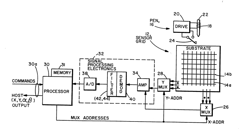
Fig. la is a block diagram of an embodiment of a digitizer
tablet that embodies the teaching of the invention;
Fig. lb is a block diagram that illustrates in greater
detail a portion of the digitizer tablet of Fig. la;
Fig. 2a depicts a first measurement sequence for a pen
positioned at a location above an array of EM tablet coils
of a type shown in Fig. lb;
Fig. 2b depicts a second meas~lrement sequence for the pen
positioned as in Fig. 2a;
Fig. 3 illustrates three sensor grid inductor
configurations, specifical]y a plurality of conductors (a);
a plurality of coils (b); and a plurality of differentially
connected coils (c);
Fig. 4a illustrates o~erlapping, differentially connected
coil pairs for an x-axis and a y-axis sensor array;
Fig. 4b shows one of the differentially connected coil pairs
of Fig. 4a and shows a connection of the coil pair to a
readout device;
Y09-92-048 6
~087768
Fig. 5 is a flowchart illustrating the method depicted in
Figs. 2a and 2b;
Fig. 6 is a flowchart illustrating a method of threading
x-axis and y-axis measurements;
Fig. 7 is a flowchart illustrating a method of the invention
wherein an additional coil is scanned before a comparison is
completed;
Fig. 8 is a graph that depicts an actual pen position and a
corresponding non-linearity in an estimated pen position;
and
Fig. 9 illustrates in greater detail the three sensor grid
inductor configurations of Fig. 3, and also shows the
waveforms induced into the inductors due to the proximity of
the pen.
DETAILED DESCRIPTION OF 'IH~; INVENTION
Referring to Figs. la and lb there is shown in block diagram
form a digitizer tablet 10. Tab]et 10 includes a sensor
grid 12 comprised of two superimposed arrays of sensing
elements, specifically an x-ax~is array 14a and a y-axis
array 14b. In this embodiment each of the sensing elements
includes an inductor. The indllctors of one array are
typically disposed in an orthogol~al manner relative to the
inductors of the other array.
As employed herein the term "inductor" is intended to
encompass an inductive loop or coil, or a single conductor
arranged in a pattern of loops or coils. The loops may be
regular in shape or irregular in shape. Multiple inductors
may be comprised of a single wire or conductor, wherein
measurement of a signal fro;n one of the inductors is made by
measuring a signa] induced across or around a particular
closed path defining that inductor. The term inductor, in
one embodiment of the invention, encompasses a pair of loops
or coils that are differentially connected to one another.
Y09-92-048 7 20~7 G~
The inductors may be adjacent to one another in a same
plane, or two or more inductors, or the loops composing two
inductors, may overlap one another. The inductors may be
formed by a discrete conductor of circular cross-section
that is comprised of copper or the like, or as, by example,
a conductive trace that is printed or otherwise formed upon
a surface of a substrate.
Also as employed herein, a coil is defined to be a conductor
forming a plurality of loops that enclose substantially the
same area.
During use, a field generating device contained within a
stylus, puck, or a pen 16, generates an electromagnetic
signal that induces a signal into the inductors of the
arrays 14a and 14b, the signal being sensed to determine a
position of the pen 16 relative to the sensor grid 12. The
pen 16 includes an inductive coil 18 and a coil drive
circuit 20. Coil 18 is typically wrapped around a ferrite
core 22. A contact switch 24 is normally employed for
indicating when the tip of the pen 16 contacts an upper
surface of the sensor grid 12.
By example, the inductors of the sensor grid 12 are provided
as a plurality of adjacently disposed coils, with each coil
having an inductance within a range of approximately 0.1 to
approximately 1.0 microhenries, ror a coil that is one
centimeter in width and approximately 20 centimeters in
length. A typical number of coils for each of the arrays 14a
and 14b is twenty. Also by example, the inductance of the
pen coil 18 is withill a range of approximately 100
microhenries to approximately 200 microhenries. The drive
circuit 20 drives the pen coil 18 with a frequency of
approximately 500 KHz The pen coil 18 is inductively
coupled to the inductors of the sensor grid 12.
Tablet 10 further inc]udes an x-axis multiplexer 26 and a
y-axis multiplexer 28 that are coupled to the coils of the
x-axis sensor array 14a and the y-axis sensor array 14b,
respectively. A particular y-axis coil is selected to be
Y09-92-048 20~7~ 6~
read out by means of a Y address signal (YADDR), and a
particular x-axis coil is selected by means of an X address
signal (XADDR), both of which are generated by a processor
30. The signal outputs from the selected y-axis coil and
the selected x-axis coil are provided to a signal processing
electronics block 32. Block 32 includes an amplifier 34
having an output that is supplied to an analog-to-digital
(A/D) converter 38, via a demodulator 40 and a filter that
includes an integrator 42 and a sample and hold (S/H) 44.
The A/D converter 38 converts the magnitude and polarity of
the analog signal to a digital format for inputting to the
processor 30.
As is seen more clearly in Fig. lb, the output of the
amplifier 34 feeds the demodulator 40, which in turn feeds
the integrator 42 and the S//H 44. The S/H 44 enables one
coil measurement to be held for digitizing by the A/D 38
while a second, subsequent coil measurement is initiated
within the preceding circuitry. For the illustrated
embodiment there are 11 x-axis coils (A-J) that have one end
coupled in common to circuit ground. A particular one of the
coils (A-J) is se]ected by the X-MUX 26 to be coupled to the
input of the filter 32 and the amplifier 34. In other
embodiments of the invention more or less than 11 coils can
be employed.
The processor 30 is connected, hy example, to an external
host by a communication line 3~a, such as a conventional
RS-232C serial communication line, and receives commands and
set up information from the host (Fig. la). In other
embodiments of the invention the sensor grid 12 and the
other components of Fig. 1 are an integral part of a
portable, battery powered data processor wherein the sensor
grid 12 and the pen 16 provide a user interface to a
handwriting recognition system. For this latter embodiment
the processor 30 may be connected to other components of the
data processor through a gener~l purpose or a special
purpose bus.
Y09-92-048 9
208~76~
The processor 30 includes a memory 31 for storing temporary
data and coil measurements, and also for storing programs,
including programs that execute a pen position estimation
and the optimal coil scanning method of the invention.
During operation the processor 30 outputs packets of
information relating to the position and, if required,
angular orientation of the pen 16 relative to the sensor
grid 12. This information includes x-axis and y-axis pen
position information, and may also include tilt information
(alpha and beta) regarding the orientation of the pen 16
relative to a sensor grid 12 x-y coordinate system. Typical
operating speeds enable approximately 100 to approximately
300 position measurements to be made per second.
Fig. 3 illustrates three sensor grid inductor
configurations, specifically a plurality of conductors (a);
a plurality of coils (b); and a plurality of differentially
connected coils (c). Fig. 3 is intended to be viewed in
conjunction with Fig. 9, which graphically depicts the
signal waveforms induced into the plurality of conductors
(a); the plurality of coils (b~; and the plurality of
differentially connected coi 15 (C~, due to the proximity of
the transmitting coil 18 within the pen 16.
The "conductor" arrangement of Figs. 3(a) and 9(a) implies a
distant return path and, thus, i-t should be realized that
each "conductor" is act~la]ly p~rt of a larger loop. This
configuration is simi1ar to t~le arrangement in the
aforementioned U.S. Patent 4,423,286. As can be seen in Fig.
9(a), the conductors located on one side of the pen have a
negative signal induced therein, and conductors on the
opposite side of the pen have a positive signal induced
therein. A zero-crossing (ZC) poin-t is an intersection of an
axis of the pen with a plane that contains the inductors.
Figs. 3(b) and 9(b) illustrate the case for a coil geometry
of a type shown in Fig. lb. As can be seen, the induced
signal on each side of the pen ]6 includes sidelobes having
a polarity that is opposite that of the main part of the
Y09-92-048 10 2 0 8 7 7 6 8
induced signal near the pen. A maximum induced signal is
approximately coincident with the pen position.
Figs. 3(c) and 9(c) illust~ate the case for a coil geometry
of a type shown in Figs 4a and 4b. As can be seen, the coil
pairs located one side of the pen have a positive signal
induced therein and coil pairs on the opposite side of the
pen have a negative signal induced therein. The induced
signal on each side of the pen 16 also includes sidelobes
having a polarity that is opposite that of the main part of
the induced signal Oll that side of the pen. The
zero-crossing of the induced signal is approximately
coincident with the pen position.
The construction and use of such differentially connected
coil pairs is described in commonly assigned U.S. Patent
Application S.N. 07/696,434, filed May 6, 1991, entitled
"Sensor Grid for an Electromagnetic Digitizer Tablet", by
Gregory F. Russell, now U.S. Patent No. 5,136,125, issued
August 4, 1992. The teaching of the invention also applies
to pairs of coils that may be coupled together in a
differential fashion by circui~ry that is external to the
array of coils.
In Fig. 9, it should be apparent that as the pen 16 is moved
over the underlying inductors that the signal waveform will
shift with the pen. As a result, different inductors will
sense different portions of the characteristic signal
waveform at different times, as a function of pen position.
It should also be realized that the shape and amplitude of
the sidelobes is highly variable, ~nd is strongly influenced
by pen tilt. Pen tilt is considered to be an angular offset
of the pen 16 away from a normal to the surface of the
underlying tablet that contains the inductors.
Three distinct embodiments of measurement determination
techniques are encompassed by the invention. These three
embodiments employ an array of adjacent sensing elements,
such as inductors, designated A, B, C, D, E, and F.
Y09-92-048 11 ~087768
A first embodiment is referred to as a three line technique
wherein inductors B and C are measured and, based on this
measurement, inductor A or D is measured.
A second embodiment is referred to as a four line technique
wherein inductors B and E are measured and, based on this
measurement, inductors (A, D) or (C, F) are measured. Or,
(B, D) are measured and, based on this measurement,
inductors (A, C) or (C, E) are measured.
A third embodiment is referred to as a two line differential
technique wherein an inductor B is measured and, based on
the polarity of the measured signa], either inductor A or C
is measured.
This latter embodiment is applicable to cases shown in Fig.
3(a) and Fig. 3(c), whereas the first two embodiments are
applicable to the case shown in Fig. 3(b).
A presently preferred method of scanning the coils of the
sensor grid 12 is now described with reference to Figs. 2a,
2b, and the flowchart of Fig. 5.
In accordance with the invention, instead of scanning a
predetermined set of coils, such as seven or more adjacent
coils, performance is improved by first measuring a single
pair of coils that are disposed near to, and which straddle,
an expected position of the pen 16. That is, one of the
selected coils is locateci on one side of the expected
position and the other one of the selected coils is located
on an opposite side of the expected position. Next, based on
the value(s) of this first measurement, a determination is
made of which additional coils are to be measured to
complete the measurement cycle so as to obtain a minimum
required number of measurements from which to interpolate
the actual position of the pen l6, relative to the array of
inductors.
In accordance with the invention the method operates to
determine a set of inductors that includes all inductors
Y09-92-048 12 ~0 8 7 7 68
that are required to compute or interpolate the actual
position of the pen 16, and includes no inductors that are
not re~uired to compute or interpolate the actual position
of the pen 16.
For the four line pen position determination method that is
illustrated in Figs. 2a and 2b the sensor grid 12 includes a
plurality of individual coils as in Figs. lb, 3(b), and
9(b), and two of the x-axis coils 14a are sequentially
measured or scanned during each portion of the measurement
cycle. The field strength (FS) induced by the pen 16 into
the underlying coils can be seen to be generally Laplacian
in shape and to have a maximum amplitude that coincides
closely with the act~al position of the pen 16. For the
illustrated example, the pen 16 is expected, based on
previous measurements, to be between the coils designated as
G and H. This expected position is based upon a previous
determination of pen 16 position (Block A, Fig. 5) or, if
the user has just begun operation with the sensor grid 12
and the pen 16, by a first step of scanning all of the coils
of the x-axis array 14a an~ the y-axis array 14b to make an
initial determination of pen 16 positlon, relative to the
sensor grid 12 (B]ock B, Fig. 5).
The scan sequence is adapted to a position estimation method
which requires measurement of four coils near, but not
necessarily including, the coil clOsest to the pen position.
The first step measures the signals from the coils F and I
in succession as Measurement 1 (M1) and Measurement 2 (M2).
That is, the first step measures two coils that are disposed
on opposite sides of, or s-traddle, the expected position of
the pen and that are separated from the expected position,
(Block C, Fig. 5). Specifically, one measurement is made to
the left (L) of the expected pen position, and one
measurement is made to the right (R) of the expected pen
position, it being realized that the terms "left" and
"right" are used for illustrative purposes only. By example,
if the sensor grid 12 is oriented vertically then one
measurement may be made from a coil that is "above" the
Y09-92-048 13
2087768
estimated pen position and one measurement may be made from
a coil that is "below" the estimated pen position.
Having completed the first measurement step, a comparison is
made between the magnitude of FS for the left coil, or coil
F for this example, and the magnitude of FS for the right
coil, or coil I for this example (Block D, Fig. 5). This
comparison provides additional information about the
position of the pen, which is used to select the remaining
coils to measure (Block E, Fig. 5).
In accordance with the example of Fig. 2a:
if FSF > FSI, then the pen is slightly to the
Left, so
next scan coils E and H in the Left direction, else
if FSF < FSI, then the pen is slightly to the
Right, so
next scan coils G and J in the Right
direction.
For the example of Fig. 2a the pen 16 is nearer to coil F
than to coil I and, thus, the FS measured for coil F is
greater than the FS measured for coil I. As a result, the
coils E and H are selected and sequentially measured during
measurement step 2 to complete the measurement cycle for the
x-axis array 14a. At the completi on of the measurement cycle
for the x-axis array 14a the processor 30 has a minimum
required number of measurements (the FS for coils E, F, H,
and I) from which to interpolate the actual position of the
pen 16 along the x-axis of the sensor grid 12.
The measurement cycle of Figs. 2a and 2b is then repeated
for the y-axis array 14b (Block F, Fig. 5). At the
completion of the y-axis measurement cycle, the processor 30
is enabled to determine an estlmated (x,y) position of the
pen 16 relative to the coordinates of the sensor grid 12,
and to output the result (Block G, Fig. 5).
Y09-92-048 14 2 o877 68
For the differentially connected coil pair embodiment of
Figs. 3(c) and 9(c), and in accordance with the two line pen
position determination met~od, the FS induced by the pen 16
into the underlying coils can be seen to go from positive
values to negative values and to pass through zero near the
actual pen position. For the illustrated example, the pen 16
is expected to be near the differentially connected coil
pair designated as I (Fig. 9(c)). This expected position is
based upon a previous determination of pen 16 position or,
if operator has just begun operation with the sensor grid 12
and the pen 16, by the first step of scanning all of the
differentially coil pairs of the x-axis array 14a and the
y-axis array 14b to make an initial determination of pen 16
position, relative to the sensor grid 12.
The first measurement step measures the signal from the coil
pair I that is, from the coil pair whose center is nearest
to the expected position of the pen.
Having made the first measurement, the polarity of the
measurement of differentially connected coil pair I is
examined. Based on this examination, a next coil pair is
selected for measuremen-t. In accordance with the example of
Fig. 9(c) and the two line clifferential determination
technique referred to above:
if FSI > 0, (positive polarity) then
next scan coi1 pair J, else
if FSI < 0, (negative polarity) then
next scan coil pair H.
At the completion of the measurement cycle, the processor 30
has two measurements from which to interpolate the zero
crossing point and the ?osition of the pen 16 along the
x-axis of the sensor grid 12.
If FSI = 0 it is known that the pen 16 is positioned over
the centerline of the differentially connected coil pair,
and a further measurement along this axis is not required.
Y09-92-048 15 2Q8~7 68
The measurement cycle is then repeated for the y-axis array
14b. At the completion of the y-axis measurement cycle, the
processor 30 is enabled to determine an estimated (x,y)
position of the pen 16 relative to the coordinates of the
sensor grid 12.
If the pen 16 is known to be in motion, as determined from
previous position estimates, the determination of the
expected position of the pen 16 may incorporate this
information to estimate the position of the pen that is
expected at the midpoint in time of the first measurement.
This expected position is based on a rate of change of pen
position and on a determined direction of pen motion. The
coil pair nearest the expected position is measured first.
If the gradient is negative, then a measurement is made of a
previous coil pair, which should have a gradient greater
than the first. If instead the first gradient is positive,
then a measurement is made of a next coil pair (to the
right), which should have a gradient less than the first.
Fig. 8 is a graph that depicts ~n actual pen position versus
an estimated pen position, and shows the non-linearity
inherent between the pOilltS labeLed (0, 0.5, and 1) for the
three inductor geometries of Fig. 3.
The conditional inductor measllrement method of the invention
yields an optimal set of coil measurements, unless the
actual pen position is more than one whole coil spacing away
from the initial coil choice. For this case, the first and
second coils do not enclose the actual pen position. In
this case, which can be expected to occur only at high pen
velocities and accelerations, the interpolated zero-crossing
position estimate will be found to be to one side of the two
measured coil pairs, but wiLl often still be sufficiently
accurate, after compensating for the non-linearities
illustrated in Fig. 8. In contrast, a non-adaptive minimal
scan will result in increased distortion whenever the pen is
on the opposite side of the first coil from the expected
position, and is thus not between the first and the second
coil pairs, as expected. For example, and referring to Fig.
Y09-92-048 16 208~
9(c), this condition would occur if the pen 16 was expected
to be between coils H and I, but was actually to the left of
coil H.
A further method of the invzntion employs the aforedescribed
coil measurement determination in the context of a technique
referred to as coordinate threading. In some EM tablet
designs the analog electronics may be structured such that
the measurement of the signal through a loop is not
available until substantially after the end of the signal
integration period. In these systems, it is useful to setup
the next loop measurement cycle, i.e. choose the next loop
to be measured, before the value is available from the last
loop measurement. In this case, the conditional scanning
method is used, without loss of time, by threading the
x-axis and the y-axis coordinate scans.
As is seen in the flowchart of Fig. 6, this is accomplished
by measuring the first x-axis loop pair (Block A) and, while
the analog signal is being digitized, the first y-axis loop
pair is measured (Block B). When the x-axis gradient value
is available, the second x-axis loop pair is selected in
accordance with the methods described above (Block C), and
is measured (Block D) while the first y-axis loop pair
measurement is being digitized. After the first y-axis
measurement is available, the next y-axis loop pair
selection is made (Block E) and me~sured (Block F) while the
second x-axis loop pair is being digitized. Thus, this
method alternates between x-axis measurements and y-axis
measurements.
Furthermore, if there are other measurements which can be
made independently of the result of the first measurement,
these measurement(s) may be made between the first and
second loop pair measurements.
As an example, the flowchart of Fig. 7 shows a case where a
decision is made to scan a first coil pair (Block A), and at
Block B the measurement is made. At Block C, and before the
result of the measurement made at Block B is available, a
Y09-92-048 ~7 2087~ 6~
further coil is measured which is known must be measured
regardless of the outcome of the decision of the first
measurement.
As an example, and using a pen estimation technique for
coils labeled A, B, C, D, and E, a first measurement step
measures the coil pair B and D, i.t being assumed that the
pen is expected to be near to coil C. In accordance with
this position estimation technique a next pair of coils will
be either A and C, or C and E. That is, regardless of the
outcome of the comparison between coils B and D, coil C will
be included within the next measurement. As a result, at
Block C coil C is measured.
At Block D the result of the measurement at Block B is
available, and a decision is made as to which coil pair
(A-C) or (C-E) is next to be measured, the decision being
based on the measurement at Block B. At Block E only coil A
or coil E is measured, in that the measurement of coil C has
already been made at Block C. At Block F the result of the
measurement at Block C is available. At Block G the result
of the measurement at B]ock E is available, and at Block H
the estimate of the position of the pen, along one axis, is
determined based on the measurements made at Blocks B, C and
E.
Although described in the context of an EM digitizing
tablet, it should be appreciated that the teaching of the
inventional also applies to electrostatic and electric field
digitizing tablets wherein the signal is electrically
induced on an array of conductors instead of inductive
loops. Furthermore, although described in the context of a
method that advantageously obtains a minimum required number
of measurements to estimate the pen position, it should be
realized that the method can also be employed to obtain
additional measurements or pairs of measurements, over and
above the minimllm requirement, such as sidelobe
measurements.
Y09-92-048 18 2 0 87 ~ ~ 8
Thus, while the invention has been particularly shown and
described with respect tc preferred embodiments thereof, it
will be understood by those skilled in the art that changes
in form and details may be made therein without departing
from the scope and spirit of the invention.