Note: Descriptions are shown in the official language in which they were submitted.
2Q~7~9
The present invention relates to a semiconduckor module as set
out in the de-fininy portions of patent claims 1 ancl ~.
Semiconductor modules of this lcind that have an electric~lly
insulating and thermally conductive layer between a semiconductor
chip and a thermal abstraction device are already familiar, for
example, from the documentation associated with the 5th
Colloquium "Verbindungstechnik in der Elektronik" [Connector
Technology in Electronics~, 1990.02.20/22, pages 25-29. In the
case of the insulating layer, this refers to an Al2O3 layer on
which intermediate layers of copper are applied on both sides
(direct copper bonding). The semiconductor chip is connected to
one intermediate layer through a solder layer and the thermal
abstraction device is connected to the other intermediate layer
through an additional solder layer or an adhesive layer.
It is the task of the present invention to describe a
semiconductor module that displays significantly less thermal
resistance between the semiconductor chip and the thermal
abstraction device than the known semiconductor modules, for a
comparable insulating capability. According to the present
invention, this problem has been solved by the features described
in the preambles to patent claims 1 and 8.
Claims 2 to 7 describe preferred embodiments of the semiconductor
module according to the present invention.
The present invention will be described in greater detail below
on the basis of the drawings appended hereto. These drawings
show the following:
igure 1: a cross-sectional representation of a known
semiconductor module;
Figure 2: a cross-sectional representation of a semiconductor
module according to the present invention, the base
~0~77~
plate of the power semiconductor struc~ur~1 element
serving as a thermal abstr~ct~on devicei
Figure 3: a cross-sectional representation of a semiconductor
module according to the present invention, the therm~l
abstraction device consisting of a heat sink;
Figure 4: a cross sectional representation of a semiconductor
module according to the present invention, as in figure
3, in which the insulating layer is applied directly to
the heat sink.
Figure l is a cross-sectional representation of a known
semiconductor module in which a DCB substrate DCB (direct copper
bonding) is located between a semiconductor chip CHIP1 and a
thermal abstraction device Wl, this DCB substrate consisting of
an insulating layer ISol that has copper intermediate layers Zll
and Zl2 applied on both sides. I`he thermal abstraction device Wl
is formed from a base plate of the semiconductor module that is,
for example, of 3-mm thick copper sheet. ~he semiconductor chip
CHIPl is connected mechanically through a connecting layer Vll in
the form of a solder layer to an intermediate layer Zl2, and
this, in its turn, is connected mechanically through a connecting
layer Vl2 in the form of a solder layer or adhesive layer to the
thermal abstraction device Wl. If one proceeds, as is typically
the casa, from a solder layer V11 that is 50 ~m thick and a
solder layer or adhesive layer V12 that is approximately 100 ~m
thick, and intermediate layers Zll and Z22, each 300 ~lm thick
and an insulating layer ISO1 of conventional ceramic such as
Al203 or AlN with a layer thickness of approximately 16 ~m, then,
given a thermal conductivity capability of copper k = 3.8 W/cm K
and a thermal conductivity capability of k = 0.3 W/cm K for Al203
together with the thermal resistance of the base plate this will
result in a unidimensional thermal resistance of Rth =
approximately 0.35 K cm2/W. Because of th~ lateral di.mensions
that become greater towards the thermal abstraction device, there
.
::
; -
,
~7~
will also be a thermal spread that e~uates to a reduction o~ -~he
effective thermal resistance.
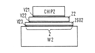
An important basic concept of the present invention is khe
simultaneous optimization of the thermal resistance of the
insulating layer and of the thermal resistance of the connecting
layers. A first embodiment of a semiconductor module according
to the present invention is shown in figure 20 This has an
intermediate layer Z2 and an insulating layer IS02 that is of
crystalline carbon (diamond) between a semiconductor chip 2 and a
thermal abstraction device W2 in the form of a base plate.
Layers of crystalline carbon are understood to be poly-
crystalline as well as mono-crystalline carbon layers, the latter
being producible, for example, by the deliberate planting of
crystallization seeds; because of the absence of any grain limits
these display better thermal conductivity capability than poly-
crystalline carbon layers. According to the present invention,
between the semiconductor chip CHIP2 and the intermediate layer
Z2, which consists of copper, for example, and which serves for
contact in the case of vertical structural elements, there is a
connecting layer V21 that is of silver. The intermediate layer
Z2 is similarly connected mechanically to the insulating layer
IS02 through a silver layer V22 and, in its turn, the insulating
layer IS02 is again connected through a connecting layer V23 to
the face area 2 of the thermal abstraction device W2. In order
to produce the semiconductor module according to the present
invention, a silver paste is applied, for example, by screen
process printing, to the intermediate layer Z2 in the area of the
contact surfaces and, in the case of the thermal abstraction
device W2, in the face area 2 and then a mechanical connection
between the semi-connector chip CHIP2 and the thermal abstraction
device W2 is ef~ected with the help of a process known in low
temperature connection technology as pressure sint~ring, which is
already known per se. When this is done, the thickness of the
layer of silver paste is approximately 10 to 100 ~m, and consists
- .
:::
~7~9~
of silver powder with plakelet-li]ce silver particles that are
suspended in cyclohexanol as a solvent. The sintering
temperature amounts, for example, to 230UC and a pressure of at
least 900 N/cm2 is exerted on the whole arrangement in a vertical
direction during a sintering time of approximately one minute.
The sintering temperature can lie in a range between a lower
limiting value of approximately 150C, and an upper limiting
value of approximately 250C. It should be pointed out that an
adequate connection of the parts that have been described is
achieved even with sintering times of a few seconds, and that -the
pressure can also be increased to l to 2 t/cm2. In order to
create sinterable surfaces in the semiconductor chip CHIP2 and
the intermediate layer Z2, a layer sequence of titanium,
platinum, and gold is vaporized or sputtered on, and the face
area 2 of the thermal abstraction device is, for example, first
nickel-plated and then silver-plated or, as in the case of the
intermediate layer, is provided with a layer sequence of
titanium, platinum and gold. If, for example, the thicknesses of
the connecting layers V21 ... V23 are, in each instance, 10 ~m,
the thickness of the intermediate layer Z2 is 300 ~m, the
thickness of the crystalline carbon layer ISO2 is lO0 ~m, and the
thickness of the base plate, as in figure l, is 3 mm, then at a
thermal conductivity capability of, for example, poly-crystalline
carbon (diamond) k = 12 W/cm K and the connecting layers of
si~ver are k = ~ W/cm K together with the thermal resistance of
the base plate, this will result in a unidimensional thermal
resistance Rth of approximately 0.1 K cm2/W. A thermal
transitional resistance that is smaller by a factor of 3 is
achieved at a comparable insulation capability.
A second embodiment of the semiconductor module according to the
present invention is shown in figure 3; this consists of a
semiconductor chip CHIP3, connecting layers V31 ... V33, an
intermediate layer ~3, an insulating layer ISO3 that is of
crystalline carbon, and a thermal abstraction device W3, the
~ .
2~7~
structure of the semiconductor module shown ~n fiyure 2 being
identical with the structure oE the semiconductor module shown in
fiyure 3 as Ear as the thermal abstraction device W3. Instead of
the thermal abstraction device W2 in -the form of a base plat~,
the thermal abstraction device W3 consists o~ a heat sink that
is, for example, of aluminum or copper, and which has a face area
3 as a sinterable surface. Using the layer thicknesses cited as
examples above, from a unidimensional approach, it is possible to
achieve a thermal resistance Rth of approximately 0.02 K/W cm2
between the semiconductor chip (CHIP3) and a face area 3 of the
heat sink.
Figure 4 shows a third embodiment of the semiconductor module
according to the present invention; in this, connecting layers
V41 and V42, an intermediate layer Z4, and an insulating layer
ISO4 of crystalline carbon are located between a semiconductor
chip CHIP4 and a thermal abstraction device W4; the insulating
layer ISO4 is grown on the face area 4 of the heat sink and the
connecting layer V42 connects the insulating layer with the
intermediate layer Z4 and the connecting layer V41 connects the
semiconductor layer CHIP4 to the intermediate layer Z4. The
embodiment shown in figure 4 differs from the embodiment shown in
figure 3 only in that the insulating layer ISO4 is grown directly
onto the heat sink W4, there being no connectiny layer between
the insulating layer and the thermal abstraction device. A
further reduction of the thermal resistance is possible by
eliminating the connecting layer and by the possibility of using
a thinner insulating layer, for example, a poly-crystalline
carbon layer with a thickness of 30 ~m that can be handled more
easily because it is grown directly on the heat sink. Before the
insulating layer is grown onto the face area 4 of the heat sink,
this area can be provided with a layer of molybdenum or aluminum,
for example. The thermal transition resistance Rth between the
semiconductor chip CHIP4 and the face area 4 of the heat sink
amounts to approximately 0.01 K/W cm2, if the thic]cnesses of the
:. .
7 .~ 9
lay~rs are select~d as in figure 2. ~or applications in which
only voltages below ~00 V occur, in addition to crystalline
carbon la~ers, it is also possible to use amorphous carbon
layers, so-called a-C:H-layers with a thickness of less than
approximately 1 ~m, although these display a lower insulation
capability and a lower thermal conductivity capability than
crystalline carbon layers.
The semiconductor modules according to the present invention are
used in the domain of power semiconductors, for example,
thyristors, in other semiconductor structural elements in which
high levels of power dissipation occur, such as, for example,
laser or high output light diodes as well as microwave structural
elements, and in IC's, in which good thermal abstraction is
required. It is also possible to dispense with the intermediate
layer of copper which is only used for contact.