Note: Descriptions are shown in the official language in which they were submitted.
~ ~ ~ 8 7 8 4 ~
Apparatus and Method for Generating a Transition
Between the On and Off States of a
Radio Frequency Transmitter
Field of the Invention
The present invention relates generally to
communications equipment, and more particularly to an
apparatus and method for generating a transition
20 between the on and off states of a radio frequency (RF)
transmitter without producing undesirable spectral
components .
Background of the Invention
A RF transmitting device, of which a digital
cellular radiotelephone mobile subscriber unit is a
convenient example, provides an appropriate setting for
30 describing the need for the present invention. FIG. 1 is a
diagram of cellular mobile subscriber units 110-112
operating in a cellular radiotelephone system 100. The
cellular system 100 is designed to supply mobile
telephone service using a "cellular" radio coverage plan.
2 2087845
This plan divides a geographical area into a number of
coverage areas or "cells" 103-109 with each cell being
assigned a portion of the available radio channels. The
channels used in one cell are again useable in spatially
5 separated cells in the same coverage area 100.
Recommended minimum standards for the digital
subscriber units 110-112 for use in the 800 MHz.
Cellular operating band may be found in the Cellular
System Dual-Mode Mobile Station-Base Station
10 Compatibility Standard IS-54 (Revision A) published by
the Electronic Industries Association in January 1991
which assures that the subscriber units 110-112 can
obtain service in any cellular system 100 that meets the
compatibility requirements of IS-54 (Revision A). For
15 the sake of brevity, all subparagraphs (or sections)
called out in this document refer to IS-54 (Revision A).
Compatibility, is used in connection with IS-54
(Revision A), is understood to mean that any subscriber
unit 110-112 is able to place and receive calls in any
20 cellular system 100, and all cellular systems 100 are
able to place and receive calls with any subscriber unit
110-1 12. To assure compatibility, it is essential that
both radio system parameters and call-processing
parameters be specified in the sequence of call-
25 processing steps that the mobile and land stationsexecute to establish calls has been specified in IS-54
(Revision A) along with the messages and signals that
are exchanged between the system provider and the
subscriber units 1 10-1 12. The subscriber units 110-
30 112 communicate with a distributed array of cell-site
land stations, for example cell-site 113. The cell-site
land station 113 is controlled by the cellular-system
network control and switching equipment 115 that
provides connection to the worldwide
7 8 4 5
telecommunications network 117. A call between the
land network 117 and the subscriber units 110-112 is
routed via the cellular control system 115 to the cell
site 113 that best serves the location of the subscriber
units 110 through 112. A call in progress can proceed
indefinitely as a subscriber unit 110, 111 or 112 moves
from cell to cell throughout the coverage area 100 since
it is automatically reassigned to an available channel
with any new cell.
The transmitters in mobile subscriber units 1 10-
112 must be capable of reducing or increasing output
power on command from a cell-site land station 113
specifying eight output power levels per 2.1.2.2 of IS-54 (Revision A). The
power level specified depends of the distance between
1~ the subscriber unit 110, 111 or 112 and the cell-site
113. For example, the output power level transmitted
from subscriber units 1 10-1 12 increases as the
distance between the subscriber units 110-112 and the
cell-site 113 increases. However, the input power to
the cell-site 113 from the subscriber units 1 10-112 is
desired to be substantially equal regardless of the
distance between the subscriber units 110-112 and the
cell-site 11 3.
Cellular radiotelephones operating in a digital
system, such as a time division multiple access (TDMA)
signalling scheme described in IS-54 (Revision A), have
a particular problem of generating a shaped transition
between the minimum and maximum output power levels
of the transmitter's power amplifier. In the TDMA
system, data for one mobile subscriber unit is
multiplexed in time with data for two other mobile
subscriber units on the same channel. The format for a
time frame of information sent by the mobile units 1 10-
112 is described in 1.2.1 of IS-54 (Revision A). Each time frame includes
''~!:~
4 ~ 2~84g
two transmit, two receive and two idle time slots. Each
subscriber unit 110-1 12 transmits a burst of
information in a transmit time slot to the cell-site 1 13.
Transmission of bursts of information by the mobile
5 unit 110, for example, requires the mobile unit's
transmitter to turn on and off at the beginning and end
of each frame, respectively. In the TDMA system the
maximum transition time between the on and off states
of the mobile units transmitter is required to be three
information symbol time periods per 2.1.2.1.2 of IS-54 (Revision A).
In general, reducing the transmission time
between the on and off states of the transmitter
increases the available time for transmission of
information but has the adverse effect of increasing
15 spectral splatter which interferes with adjacent and
alternate channels assigned to other subscriber units.
Adjacent and alternate channel interference
specifications, -26 dbc and -45 dbc respectively, are
described in 2.1.4.1.2 of IS-54 (Revision A). Increasing the ~a~sition time
20 reduces the spectral splatter but shortens the available
time for transmission of information. Therefore, a
compromise is needed between acceptable spectral
splatter and required time for data transmission. For a
TDMA system, simply turning the transmitter on or off
25 with a step function within the maximum transition
time will not meet the spectral splatter requirement.
In the TDMA system, the transmitter is specified
to operate over a wide dynamic range of 94.8 dB.
Voltage controlled attenuators (VCA) typically used to
30 control the magnitude of the power output signal have a
dynamic range of 35 dB. Three cascaded VCAs may be
used achieve a dynamic range of 105 dB thus meeting the
dynamic range requirement of 94.8 dB. The problem with
this approach is that additional signal processing and
5 20g7~45
hardware is required to shape the transition between
the on and off states using a digital signal source.
Furthermore, it is advantageous to implement the VCAs
on an integrated circuit (IC) but there are problems
5 achieving the full dynamic range required due to the
close proximity of cascaded VCAs on the IC.
Since the transmitter line up in a TDMA system is
linear, the dynamic range of the transmitted signal may
also be achieved by controlling various stages of the
10 transmitter line up. The disadvantage of this approach
is that additional control circuitry and signal processing
would be required to control the shaped transition
through the various stages thus increasing the cost and
complexity of the transmitter.
For many situations, for which a digital cellular
radiotelephone mobile subscriber unit operating in a
TDMA system is merely an example, the prior art has not
produced an apparatus or method of generating the
transition region between the minimum and maximum
20 output power levels of a RF power amplifier to meet the
difficult requirement of minimizing spectral splatter
while providing for the advantage of an economical
transmitter design.
7 ~ 4 5
- 6 -
Summary of the Invention
A method and apparatus of the present invention generates a digital burst
signal in a transmitter. The digital burst signal defines a predetermined time
duration including a first, a second and a third time period. The first time
period provides a first transition time during which the transmitter is permitted
to adjust between first and second output power levels. The second time period
provides a tr~nsmi~ion time during which the transmitter is permitted to
transmit a predetermined number of sequential symbols at the transmitter's
second output power level. The third time period provides a second transition
time during which the transmitter is permitted to adjust between the second and
first output power levels.
A first set of predetermined number of sequential symbols is generated
which are sequentially followed by a second set of predetermined number of
sequential symbols, which are sequentially followed by a third set of
predetermined number of sequential symbols. Each of predetermined number
of sequential symbols in the first and third sets of predetermined number of
sequential symbols have a zero value.
The generated predetermined number of sequential symbols are filtered
responsive to a predetermined impulse response having a leading portion and
2 o a trailing portion.
The timing of when the first, second and third sets of predetermined
number of sequential symbols are generated is controlled by the generation of
the first set of predetermined number of sequential symbols responsive to the
predetermined impulse response. The first set of predetermined number of
sequential symbols sequentially followed by the second set of predetermined
number of sequential symbols are generated at a predetermined time for loading
into predetermined taps forming the leading portion of the predetermined
impulse response to cause the transmitter to adjust between the first and secondoutput power levels only during the first transition time. The second set of
3 o predetermined number of sequential symbols sequentially followed by the third
set of predetermined number of sequential symbols are generated at a
8784 5
- 6A -
predetermined time for loading into predetermined taps forming the trailing
portion of the predetermined impulse to cause the transmitter to adjust between
the second and the first output power levels only during the second transition
time.
7 2087845
Brief Description of the Drawings
FIG. 1 is a diagram of cellular mobile subscriber
units 110-112 operating in a cellular radiotelephone
system.
FIG. 2 is a block diagram of a subscriber unit 210
used in the cellular system of FIG. 1.
FIG. 3 illustrates the channel time frame structure
including transmit, receive and idle periods for the
subscriber unit of FIG. 2.
FIG. 4 illustrates a waveform of the output power
level versus time for a transmit time slot (T) in the
time frame illustrated in FIG. 3.
FIG. 5 is a simplified block diagram of a
transmitter 500 line up used in the transceiver unit 203
of FIG. 2.
FIG. 6 is an abbreviated block diagram of a finite
impulse response (FIR) filter used in the block diagram
of FIG. 5.
FIG. 7 is a graph representing magnitude versus
time for a square root raised cosine finite impulse
response for the FIR filter of FIG. 6.
Tables 1A and 1B illustrate the input data to the
FIR filter of FIG. 6 having thirty two taps.
FIG. 8 is a flow chart describing the process used
by digital signal processor 501 to generate the shaped
transition between the minimum and maximum power
levels of the waveform illustrated in FIG. 8.
~ 8 2087845
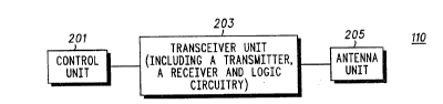
Detailed Description of a Preferred Embodiment
Referring now to FIG. 2, there is shown the
subscriber unit 210 required for a cellular system, such
5 as described in FIG. 1, which consists of the following
units: a control unit 201, a transceiver unit 203
(including a transmitter, a receiver and logic circuitry),
and an antenna unit 205. Although FIG. 2 depicts the
control unit 201, the transceiver unit 203 and the
10 antenna unit 205 as three separate units, all three may
be contained within a single housing if the physical
limitations permit either mounting the combined unit
within reach of the vehicle operator, or using it as a
hand-held "portable" unit.
The control unit 201 is the interface between the
subscriber and the system. The subscriber interface
requirements may include a handset; a keypad; a
loudspeaker; all subscriber-unit controls; indicators;
and, if provided, a digit display, with which the
20 subscriber interacts during the process of placing or
receiving a call. Portions of the control unit 201 may be
mounted physically in separate packages. A microphone
and loudspeaker combination or other peripherals may be
used in place of the handset to provide a means of using
25 the system without holding the handset. For example, a
control unit is shown and described in Motorola
instruction manual number 68P81066E40, entitled
"DYNATAC Cellular Mobile Telephone 800 MHZ
Transceiver," (or the portable transceiver shown and
30 described in Motorola instruction manual number
68P810~4E60, entitled "DYNATAC Cellular Portable
Telephone G-Series") published by and available from
Motorola C & E Parts, 1313 East Algonquin Road,
Schaumburg, Illinois 60196.
- 9 ~D Z ~
The transceiver unit 203 includes a transmitter
500, a receiver and logic circuitry with a
microprocessor and memory for providing duplex voice
transmission and reception. The radio frequency (RF)
5 band is divided into two separate 25 MHz wide segments
each consisting of 833 channels. The first segment
from 824 to 849 MHz, contains the subscriber-unit
transmit channels. The second segment from 869 to 894
MHz, contains the subscriber-unit receive channels.
10 Each subscriber-unit transmit channel is separate from
its duplex receive channel by 45 MHz.
The antenna unit 205 connects to the transceiver
unit 203 and consists of a vertically-polarized broad-
bandwidth antenna. The antenna unit 205 radiates RF
15 signals from the transmitter of the transceiver unit 203
or receives RF signals for the receiver of the
transceiver unit 203.
Referring now to FIG. 3, there is shown a signaling
frame including transmit and receive information for
20 the subscriber unit 110 operating in a TDMA system per
1.2 of IS-54 (Revision A) the frame shall consist of six equally sized time
slots, 303-308, exactly 162 symbols in length. Two
slots are designated for transmitting information, 303
and 306. Two slots are designated for receiving
25 information, 304 and 307. Two slots are designated as
an idle state, 305 and 308. In the TDMA system one
frame equals 1994 bits (972 symbols) equals 40 ms or
25 frames per second. Thus, each slot equals 6.67 ms.
Each full rate traffic channel utilizes two equally
30 spaced time slots of the frame (303 and 306, 304 and
307, or 305 and 308). Each half-rate traffic channel
shall utilize one time slot of the frame. Thus, the
transmitter must turn on and off at the beginning 309
and 313 and end 311 and 315, respectively, of each
, ~
10 ~ 2 ~ ~ 7 8 4 ~
transmitting slot 303 and 306 so as not to interfere
with adjacent receive and idle time slots. The
transmitter 500 employing the present invention
essentially meets the spectral splatter requirement
using a novel apparatus and method for generating a
shaped transition between the on and off states of the
transmitter.
Now referring to FIG. 4, there is shown a graph of
the output power level 401 of the transmitter 500
versus time 403 for the transmit time slot 303, for
example. On the time axis 403, a maximum effect point
(MEP) of the transmitted symbols is recorded. The MEP
is defined to be the point in time at which the pulse
shaping function associated with the modulation is at a
1 5 m~imllm for the symbol of interest (refer to 2.1.3.3.1 of IS-54 (Revision A)
for a description of the pulse shaping function). The
relationship between the MEP and the associated symbol
period is such that the MEP is defined to occur at the end
of the symbol period.
The first MEP for a transmitted channel is at point
6. Decoding the phase change from point 6 to point 7
provides the first two bits of transmitted data.
Decoding the phase change from point 161 to point 162
provides the last two bits of transmitted data. Point 0
is the same MEP as point 162 of the previous time slot.
A transition between the off state 405 and the on
state 407 of the transmitter's output power level is
specified to occur within three symbol periods during
transition region 409 (between MEP 3 and MEP 6).
Likewise, the transition between the on state 407 and
the off state 405 of the transmitter's output power
level is specified to occur within three symbol periods
during transition region 411 (between MEP 162 and MEP
3). When the transmitter 500 is in the on state 407,
,
~,
1 1 i
156 symbol periods or 157 MEPs are transmitted in
region 413. In the preferred embodiment of the present
invention, the maximum output power level, defined as
the on state of the transmitter, is variable between 7.8
dBm and 34.8 dBm in 4.0 dB steps per 2.1.2.2. of IS-54 (Revision A) to
achieve the output power levels 0-7. The minimum
output power level, defined as the off state of the
transmitter 500, is specified to be -60 dBm per
2.1.2.1.2 of IS-54 (Revision A) Thus, the transmitter 500 is specified to have
a maximum dynamic range of 94.8 dB (34.8 dBm minus -
60 dBm) and a minimum dynamic range of 67.8 dBm (7.8
minus-60dBm) between the off state 405 and on 407
state of the transmiKer output power level. Therein
lies the problem of achieving the maximum dynamic
range (94.8 dB) of transmitter output power level while
meeting the spectral splatter requirement.
In the the preferred embodiment of the present
invention, a novel shaped transition is produced by the
transmitter 500 between the off state 405 and on 407
state during predetermined three transitional symbol
periods which achieves the maximum dynamic range
required of the transmitter and meets the spectral
splaKer requirement. The novel apparatus and method
generating the shaped transition between the on state
405 and off state 407 of the transmitter includes two
shaped portions. The shaped transition between the off
state 405 and the on state 407 includes a first shaped
portion 415, a step function, occurring at the MEP 3
between the minimum output power level 405 and an
intermediate power level 419. The second shaped
portion 417 is a square root raised cosine (SQRC)
impulse response between the intermediate output
power level 419 and the maximum output power level
407. Likewise, the shaped transition between the on
A
12 ~ 7 ~ ~ ~
state 407 and the off state 405 includes a first shaped
portion 417', a square root raised cosine (SQRC) impulse
response, between the maximum output power level 407
and an intermediate power level 419. The second shaped
5 portion 415', a step function occurring at MEP 3, is
between the intermediate output power level 419 and
the minimum output power level 405.
For the preferred embodiment of the transmitter
500, it was determined that an instantaneous power
10 output level step, between the minimum output power
level 405 and the intermediate output power level 419,
to -20 dBc of the maximum output power level 407 met
the spectral splatter interference specification.
Therefore, the step function 415 or 415 has a maximum
15 output power level of 14.8 dBm (34.8 dBm minus 20
dBm) resulting in a maximum dynamic range of 74.8 dB
(14.8 dBm minus -60 dBm), and a minimum output power
level of -12.2 dBm (7.8 dBm minus 20 dBm) resulting in
a minimum dynamic range of 47.8 dBm (-12.2 dBm minus
20 -60 dBm).
Referring now to FIG. 5, there is shown the
transmitter 500 used in the transceiver unit 203. A
digital signal processor (DSP) 501 processes signals
from the control unit 201 and generates a corresponding
25 serial bit stream, otherwise known as a data burst, to
be transmitted within time slots 303 and/or 305 of the
signaling frame illustrated in FIG. 3. An encoder 505
converts two consecutive bits of the serial bit stream
signal 303 into a symbol corresponding to a position on
30 a ~/4 shifted DQPSK phase constellation represented by
vectors I and Q (refer to 2.1.3.3.1 of IS-54 (Revision A) for details on the bit
to symbol conversion). Signal vectors I and Q are
processed through finite impulse response (FIR) filters
507 and 509, respectively, to eliminate harmonic
13 2~784~
distortion generated by changing symbols. Digital to
analog converters (DAC) 511 and 513 convert digitally
filtered vector signals from the Fl R filters 507 and 509,
respectively, to analog vector signals. The analog
5 vector signals from the DACs 511 and 513 are combined
in mixers 515 and 517 with a first local oscillator
frequency signal from a first local oscillator 519 of 90
MHz. The local oscillator frequency signal 521 is phase
shifted by a 90 degree phase shifter 523 for mixer 515
10 since the vector signals I and Q are 90 degrees out of
phase from one another. The output of mixers 515 and
517, I and Q respectively, represent analog frequency
shifted vector signal components of the symbol to be
transmitted. Signals 1 and Q are combined in a summer
15 525 so that the vector component signals 1 and Q can be
transmitted on the same RF channel.
The output 527 of summer 525 represents an
information symbol to be transmitted by the
transmitter. The symbol 527 is then processed through
20 a voltage control attenuator (VCA) 531 responsive to an
analog voltage control line at 533. A digital voltage
control at line 535 is generated by the DSP 501 is
converted through a DAC 537 to produce the analog
voltage control line at 533 for controlling the VCA 531.
25 The attenuated signal 539 from the VCA is combined in
mixer 541 with a second local oscillator frequency
signal of 914-939 MHz from block 540 to convert the
frequency of the attenuated signal 539 from 90 MHz to
824-849 MHz at line 543. A power amplifier 545 is
30 turned on and off by a bias control signal at line 553
from the DSP 501. The power amplifier 545 amplifies
the power of the frequency shifted signal 543 to produce
an amplified signal at 547. The amplified signal 547 is
processed through a bandpass filter 549, 25 MHz wide
~ 2 ~1 8 7 ~ 4 !~
14
for example, to quiet transmit noise in other mobile
receivers. The filtered signal 551 is transmitted to the
antenna unit for radiation to the cell-site land station
113. The operation of the VCA 531 and the power
5 amplifier 545 is described in more detail in the
C~n~ n Patent Application No. 2,072,582 filed on December 18, 1991.
The transmitter 500 shown in FIG. 5 is used to
transmit digital signals. The advantage of the present
invention utilizes this conventional arrangement to
10 achieve the shaped transition between the on and off
states of the transmitter's output power level as
described in FIG. 4 while meeting the wide dynamic
range and spectral splatter requirements. In general,
the data burst generated by the DSP 501 at line 503 is
15 filtered at blocks 507 and 509 to produce the shaped
transition between the on and off states of the
transmitter 500. The maximum dynamic range (74.8 dB)
of the step function 415 or 415', as shown in FIG. 4, is
achieved using the FIR filters 507 and 509, the VCA 531
20 and the power amplifier 545. The VCA contributes to
about 35 dB of the dynamic range. The step function
415, per FIG. 4, is generated by adjusting the VCA 531
via the control line 533, enabling the FIR filters 507 and
509, and biasing the power amplifier 545. Similarly,
25 the step function 415' is generated by adjusting the VCA
531 via the control line 533, disabling the FIR filters
507 and 509, and unbiasing the power amplifier 545.
The variable output power levels 0-7 selected by control
signal levels from the cell-site 113, per FIG. 1 are
30 achieved by adjusting the VCA 531 via the control line
at 533 when the transmitter is turned on. The dynamic
range of the shaped portion 417 and 417 (per FIG. 4), a
minimum of 20 dB down from the maximum output power
level, is achieved using the FIR filter 507 or 509. The
20878~5
shaped portion 417, per FIG. 4, is formed by sending data
to the FIR filters at the MEP 3, per FIG. 4, such that the
first information symbol may be transmitted at MEP 6,
per FIG. 4. Similarly, the shaped portion 417', per FIG. 4,
5 is formed by sending data to the FIR filters at the MEP
162, per FIG. 4, such that the last information symbol
may be transmitted at MEP 3, per FIG. 4. Thus, a primary.
advantage of the present invention is that the full
dynamic range of the transmitter's output power level
10 and the spectral splatter requirement is achieved with
minimal complexity in the transmitter 500.
The transmitter 500 of FIG. 5 illustrates the
baseband data burst signal at line 503 having in-phase I
and quadrature-phase Q components filtered before the
15 modulation circuitry (comprising the mixers 515 and
517, the phase shifter 523, the summer 525 and the
first local oscillator). The apparatus and method of the
present invention of generating the shaped transition
may also be implemented by filtering a signal modulated
20 onto a carrier at a predetermined frequency that is
generated after the modulation circuitry.
An abbreviated conventional block diagram of the
FIR filters 507 and 509 shown in FIG. 6. The FIR filter
507 or 509 has 32 taps Tap1-Tap32, delay blocks D1-
25 D31, 32 coefficients C1-C32 and a summer 603. The
vector signal I or Q from the encoder enters the FIR
filter at 601 and is subsequently delayed by a
predetermined unit time delay as it passes through delay
blocks D1-D31. The vector signal in each tap location
30 Tap1-Tap32 is multiplied by a corresponding coefficient
C1-C32. The result of the multiplying each tap by a
corresponding coefficient is added together in summer
603 to produce the filtered output signal 605 of the FIR
filter 507 or 509. In the preferred embodiment of the
16 ~ 7 ~ 4 !g~
, .
present invention, FIR filters 507 and 509 were chosen
to have 32 taps for achieving the requirements of
adjacent and alternate channel interference performance
per 2.1.4.1.2 of IS-54 (Revision A) aIld error vector magnitude perf~ ce
per 2.1.3.3.1.3.3 of IS-54 (Revision A). The ~ansmitter 500 samples each
symbol from the encoder 505 of FIG. 5 four times. This
sampling rate is implemented by entering the vector
signal I or Q, representing a component of the symbol,
followed by three zeros into the FIR 507 or 509,
respectively. Thus, the FIR filter may contain at most
eight symbols among the thirty two taps (eight samples
plus twenty four interspersed zeros).
The FIR filters 507 and 509 have linear phase and
square root raised cosine (SQRC) impulse response per
2.1.3.3.1 of IS-54 (Revision A). This is produced by the impulse response
shown in FIG. 7. The SQRC impulse response is
illustrated on a graph having signal magnitude
represented on axis 702 and time represented on axis
701. Sampled magnitude vectors C'1-C'32 of FIG. 7
correspond to the coefficients C1-C32 of FIG. 6. C'17 is
designated as the MEP for the SQRC impulse response.
As previously described with FIG. 4, the MEP is defined
to be the point in time at which the pulse shaping
function associated with the modulation is at a
maximum for the symbol of interest. In the preferred
embodiment of the present invention, MEP 16 and MEP 17
are on each side of the maximum point of the response
so sampled magnitude vector C'17 is designated the MEP
of the SQRC impulse response. Four vector magnitude
samples in time, for example C'1-C'4, characterize one
symbol time for signal component I or Q of FIG. 5. Thus,
the SQRC impulse response represents eight symbols
each sampled four times such that four symbols are
sampled on each side of the MEP at C' 17.
17 20~784~
The eight symbols sampled four times each
representing the impulse response of FIG. 7 also fills
the thirty two tap FIR filter 507 or 509 of FIG. 6. One
may perceive how the four sampled symbols represented
5 by magnitude vectors C'1-C'16 in FIG. 7, having
sequentially increasing magnitudes, processed through
the FIR filters 507 and 509 of FIG. 5, produces the
shaped transition 417 of FIG. 4. In the preferred
embodiment of the present invention, the MEP at C'17 of
10 the SQRC impulse response aligns in time with the MEP 6
of FIG. 4. Since the SQRC impulse response of FIG. 7 has
four symbols to the left of the MEP at C'17 the first
symbol is entered into the FIR filter 507 or 509 at MEP
2 (MEP 6 minus MEP 2 equals four symbols) of FIG. 4.
15 Likewise, one may perceive how the four sampled
symbols represented by magnitude vectors C'17-C'32 in
FIG. 7, having sequentially decreasing magnitudes,
processed through the FIR filters 507 and 509 of FIG. 5,
produces the shaped transition 417' of FIG. 4. In the
20 preferred embodiment of the present invention, the MEP
at C'17 of the SQRC impulse response aligns in time
with the MEP 162 of FIG. 4. Since the SQRC impulse
response of FIG. 7 has four symbols to the right of the
MEP at C 17, zeros are entered into the FIR filter 507 or
25 509 at MEP 158 (MEP 162 minus MEP 158 equals four
symbols) of FIG. 4. Since the corresponding magnitude
of the vectors C'29-C'32 of the last symbol is very
small, the vectors are truncated from the impulse
response of the shaped portion 417' of FIG. 4.
30 Truncating the last of the four symbols does not
substantially affect the spectral splatter requirement
and is not needed for the shaped transition 417' since
the transition region 411 has a duration of only three
symbols.
~ 18 20878~
Tables 1A and 1B, combined, illustrate the I or Q
sampled symbols entered to the FIR filter 507 or 509,
respectively. Only the beginning Table 1A and the end
Table 1B of the table are shown to illustrate data
5 processed through the FIR filters during the transition
regions. The sampled symbols, processed through the
FIR filter at the appropriate time, generates the shaped
transition 417 during time period 409 when turning the
transmitter on and the shaped transition 41 7' during the
10 time period 411 when turning the transmitter off.
Tables 1A and 1B have 32 taps corresponding to the 32
taps of the FIR filter 507 or 509. Each symbol is
entered into the FIR filter followed by three zeros.
Table 1A describes the symbols, for example "a",
15 "b", "c", "d" and "e", entered in the FIR filters 507 and
509 during the transition from the off state to the on
state of the transmitter to generate the shaped
transition 417 of FIG. 4. Before the first symbol is
entered, the power amplifier 545 of FIG. 5 is biased off
20 via bias control signal at line 553 and the VCA 531 is
adjusted to maximum attenuation via control signal at
line 533. The FIR filters 507 and 509 of FIG. 5 are also
turned off by setting the coefficients C1-C32 per FIG. 6
to zero. As previously mentioned with FIG. 7, the first
25 symbol "a" is entered into the FIR filter 507 or 509 in
Tap1 at MEP 2 per FIG. 4. The second, third and fourth
samples of the first symbol "a" corresponding to the MEP
2 is entered into the FIR filter at taps 1, 2, and 3 as
zeros moving symbol "a" to Tap 4. The next symbol
30 entered into the FIR filter is symbol "b" at the MEP 3 per
FIG. 4 in tap 1. The MEP 3 is the beginning of the
transition region betwesn the off state 405 and on state
407 of the transmit output power level. At the MEP 3,
the VCA 531 is adjusted by the control signal at line
19 20~7~5
533 per FIG. 5 corresponding to the output power level
requested via control signal levels from the cell-site
113 of FIG. 1, and the power amplifier 545 is biased on
by bias control signal at line 553 per FIG. 5. The FIR
5 filters 507 and 509 are also turned on by setting the
coefficients C1-C32 per FIG. 6 to their corresponding
magnitude vector C'1-C'32 of FIG. 7. Adjusting the VCA
531 and biasing the power amplifier 545 allow non-
linearities and inefficiencies in the transmitter line up
10 circuitry of FIG. 5 to generate the step function 415 of
FIG. 4 from the minimum power level 405 to an
intermediate power level 419 per FIG. 4. The step
function 415 constitutes the first novel portion of the
shaped transition region 409 between the on and off
15 states of the transmitter 500. It has been empirically
determined that the step function 415 will not result in
spectral splatter violating adjacent and alternate
channel interference requirements. Also at the MEP 3,
the FIR filters are turned on by enabling the coefficients
20 C1-C32 of the FIR filters 507 and 509 as determined by
the vector magnitude C 1- C'32 of the impulse response
of the FIR filters per FIG. 7. The shaped transition 417
of FIG. 4, between the intermediate power level 419 and
the maximum output power level 407, is generated by
25 processing symbols "a", "b" and "c" and "d" through the
active FIR filters 507 or 509. Symbols "a", "b" and "c"
are shifted through the FIR filters 507 and 509 by
sequentially entering the additional symbols into the FIR
filters 507 or 509. At the MEP 6 as shown in FIG. 4, the
30 transmit output power level is at its maximum 407 and
the symbols may be transmitted. The MEP 6 corresponds
in time with the MEP of the SQRC impulse response C'17
of FIG. 7 when the first symbol "a" is in Tap17 of the FIR
filter 507 or 509. Thus, processing symbols through
20~7~45
the FIR filters 507 and 509 at a predetermined time
before the first symbol is transmitted generates the
shaped transition 417, corresponding to the impulse
response of the FIR filters per FIG. 7, in the region 409
5 between the off state 405 and the on state 407 of the
transmitter 500.
Table 1B describes the symbols "s" through "z"
entered into the FIR filters 507 or 509 during the
transition from the on state 407 to the off state 405 of
10 the transmitter 500. The beginning of the ramp down
transition occurs at MEP 162 as shown in FIG. 4. Since
the FIR filters can hold eight samples at a time, zeros
are entered into the FIR filter at MEP 158 as described
with FIG. 6. The coefficients C1-C32 of the FIR filter of
15 FIG. 7 corresponding to magnitude vectors C'1-C'32 of
the SQRC impulse response of FIG. 7 are multiplied by
Tap 1-Tap 32 as the sampled symbols are entered into
the FIR filters, respectively, until the MEP 3 at the end
of the ramp down portion 411 of FIG. 4 is reached. At
20 MEP 162 of FIG. 4, Tap 17 corresponding to the
magnitude vector C'17 of FIG. 7, the shaped transition
417' from the maximum output power level 407 and the
intermediate output power level 419 begins. As the
samples are processed through the FIR filters 507 or
25 509, the SQRC impulse response generates the shaped
transition 417'. At the MEP 3, the step function 415'
from the intermediate output power level 419 to the
minimum output power level 405 is generated by
adjusting the VCA 531 to a minimum output power level
30 via control signal at line 533 and biasing off the power
amplifier 545 via bias control signal at line 553. Since
the magnitude vectors C 29-C'32 of the last symbol "z"
are very small, their value is truncated from the
filtered response by adjusting the VCA 531 to its
21 20~45
minimum power level and biasing off the PA 545 before
the last symbol "z" has filtered through the FIR filter
507 or 509 of FIG. 5. Thus, processing symbols through
the FIR filters 507 or 509 for a predetermined time
5 after the last symbol is transmitted generates the
shaped transition 417', corresponding to the impulse
response of the FIR filters, in the region 411 between
the on state 407 and the off state 405 of the
transmitter 500.
FIG. 8 is a flow chart carried out by the DSP 501 to
implement the process of the present invention. The
process begins at block 801 whereafter a sample is
loaded from the encoder 505 into the FIR filter 507 or
509 per FIG. 5 at block 803. A determination is made at
15 block 805 if the beginning of the on state transition
region 409 has been reached. At this point in time the
fifth tap location of the FIR filter contains a MEP
sample. Tap 5 corresponds to the first symbol "a" in
FIG. 8 aligned in time with MEP 3 of FIG. 4. So the
20 transition between the on state and the off state of the
transmitter 500 may begin. If the determination is
negative, all taps are multiplied by zero at block 807
and another sample is loaded from the encoder 505 into
the FIR filter 507 or 509 at block 803. If a positive
25 determination is made at block 805, the VCA 531 is
adjusted to meet the output power level requirement
determined by the cell-site 113 of FIG. 1 and the power
amplifier is biased on at block 809 to step the
transmitter 500 from the off state 405 to the
30 intermediate output power level 419 of FIG. 4. At block
811 the Tap1-Tap32 of the FIR filter 507 and 509 are
multiplied by coefficients C1-C32, respectively, per FIG.
6. The coefficients C1-C32 correspond to the magnitude
vectors C'1-C'32 of the impulse response of each
22 2D~7-8~
sampled symbol. A determination is made at block 813
if the last symbol to be transmitted has been entered
into the FIR filter 507 or 509. If the determination is
negative, another sample of a symbol is loaded from the
5 encoder into the FIR filter at 803. If the determination
is positive, the input to the FIR filter is loaded with a
zero at block 915. As previously described with FIG. 7
and FIG. 8, the last four symbols transmitted are used to
generate the shaped transition 417' when the
10 transmitter 500 is turning off. Thus, during the
generation of the shaped transition 417', the entered
zeros behind the last symbol prevent information
symbols from being transmitted. A determination is
then made at block 817 if the end of the off state
15 transition region 411 has been reached. This occurs at
MEP 3 which is three symbol time periods past the last
transmitted symbol at MEP 162 as described in FIG. 4. If
the determination is negative the process continues to
load zeros into the input of the FIR filter 507 or 509 at
20 block 815. If the determination is positive at block 917,
the control signal at line 533 adjusts the VCA 531 a
minimum output power level and the power amplifier is
biased off at block 819 to produce the step function
415' between the intermediate output power level at
25 419 and the off state at 405 as shown in FIG. 4. The
flow then continues to block 821 to initiate normal call
processing routines.
While the transmitter 500 utilizes a stepped
transition incombination with a shaped transition to
30 complete the transition between the on and off states of
the transmitter, a shaped transition may be used to
complete the transition without utilizing the stepped
transition shown as waveshapes 421 and 421' in FIG. 4.
23 2iD87~
Appendix
Contents: Table 1 A and Table 1 B.
20~78~
IL ~D o o o O ~E ~ - - - -, ~ - - - - ~ - -
C ~) C
~ o o
~ m m
o
o
N
N
N
N
~ ~ .
N
N
N
N
N
l~ ~ O
D
-
~ ~ n
N m D
-
111 D
O ~ D ' ' '
D U
~J ~J D O
~I D O
~D ~J D O
0 rJJ D O 1
~r ~ n ., ~
~J ~ D O 'O
N ~ D O ~
_ r~/ D C~ ~ ~
_ N ~ ~ _ N ~7 ~ _ N ~7 ~ _ N ~
~ j~....................... ...
~ N ~ ~ ~ ~ ~ ~ ~ q ~ ~ ~ u~
d~-
2087~5
o . ................................... oooo
-
... ~...................................... ~
in
~,~ 0 ~ X >. ~J
~ 0 , , ~ X
o 0 , , ~ X ,.
N 0 -- ~ ~ 3 X ~ ~.1
m _ ~ ~ ~ x ~
N -- ~ ~ ~ X :~ "
N -- ~ ~ ~ X ,. ..
N -- ~ ~ ~ X ~ ,~,
N ~ ~ 3t ~
N ~ 3 X ~ "
N ~ ~ ~ x ~ ,~
N ~ ~ ~ x ~ ,~
N ~ ~t X ~ ",
0 ~ ~ X ~ ~
x ~ ~ m
r~ ~ 3 x
X
X
X ~,
_ ~ X
X ~,
~ X ~-
O~ X
~_ ~. N
~t
_ r~
_ N ~'~ ~ _ N t~ ~r _ N ~ t _ N t~ ~t _ N ~ ~t _ N ~ ~t _ N ~ ~ -- N
~..............................
~
~} m o> c~ _ N
_ _ _ ~D . . ~D . ' ' _ ' ' ' N ~ ' ' ~~ ' '