Note: Descriptions are shown in the official language in which they were submitted.
2~X~
SCG-435
~OR~LESS VIGITIZ~R WITH SYNC SI~NA~ GENERATO~
This invention relates to digitizer tablets, and in par-
ticular to cordless digitizer tablets which require a sync pulse
for proper operation.
Backaround Of Invention
Digitizing tablets are known which use sync pulses as
references to optimize performance. Several such digitizer types
are described and illustrated in commonly-assigned U.S. PatQnt
Nos. 4,952,757 and 4,990,726. These are of the electromagnetic
type, and their cursor is pulsed at regular intervals, and fol-
lowing each pulse one of the conductors of the tablet grid is
connected to a signal processing system to determine the mag-
nitude or phase of the signal voltage induced therein. To
determine the proper time to scan each conductor of the grid, a
signal ~ 8 derived from the circuitry generating the cursor
pulse~. This signal, known as the sync signal, is easily genera-
ted and used to control the scanning circuits when the cursor is
physically wired to the tablet.
In other types of digitizer tablets described and il-
lustrated in commonly-assigned U.S. Patent Nos. 4,996,393 and
5,066,833, a sync pulse is also generated when the cursor is
pulsed for the purpose of controlling sample and hold circuits
(S/H) for sampling the induced signals in the grid conductors at
an optimum time to reduce noise and interference. Again, no par-
SC~.435.000.6 -1-
.. .
. - ~ ' ' . . ' ' ' ' . ' ~
.
ticlllar problem is entailed in generating the sync signal when
the pointing devlce i~ physically wired to the tablet.
A problem does arise, however, when a cordless pointing
device i8 used, because the pointing device clrcuitry is phy~i-
cally i~olated fro~ the tablet signal processing circuitry.
Hence, it is difficult to generate in the tablet a sync signal
properly timed with respect to the timing of the pointing device
driving pulses.
U.S. Patent No. 4,795,858 describes obtaining reference
phase pulses from a signal induced in an additional auxiliary or
third grid provided in the tablet grid structure.
Summary Of Invention
An object of the invent~on is an improved digitizer
tablet construction employing a cordless pointing device and of
the type requiring a reference or sync signal for proper process-
ing oP the induced signals representing location of the pointing
device.
In accordance with one aspect of the present invention,
in a digitizer tablet of the type employing a grid system made up
of active conductors that can be selectively connected to ~ loca-
tion detector using a sync signal for determining the location of
a pointing device, the sync signal used in the location detector
at any particular point in time is derived from an active grid
conductor other than the grid conductor actually connected to the
location detector at the same point in ti~e. The underlyinq con-
cept is based on the recognition that the pulsinq of the pointing
SC~.435.000.~ -2-
2 ~
device induces signal3 in each of the actlve conductors of the
gricl system. Location signals are derived by connecting ind~vid-
ual conductors to the location detector~ and, in tha usual way,
the magnitude of the location s~gnals can be used to deter~ine
the pointing device location, the largest magnitude signals
generally being induced in the conductors closest to the pointing
device. But, since, in general, only one or a few active con-
ductors at a time are connected to the detector, the other non-
connected active conductors will also have signals induced there-
in, and these signals can be used as ~he sync pulse since they
are generated by the same pointing device pulse. To implement
this aspect of the invention, appropriate selection circuitry is
provided under the control of a microprocessor so that the sync
signal processing circuit will always be connected to a grid con-
ductor different from the grid conductor then connected to the
location signal processing circuit. This implementation con-
templates grid systems employing a one-dimensional grid, as well
as two or more dimensional grids.
In accordance with another aspect of the invention, in a
digitizer tablet of the type described employing X and Y grid
structures for determining the X-Y coordinates of the pointing
device, a conductor of one of the X and Y grids i~ used as the
source of the sync signal when a conductor of the other grid i~
used to obtain the pointing device location signal. This ar-
rangement has the advantage that it is easier to pick the con-
ductor with the strongest signal to use as the sync signal
SCG.435.000.6 -3-
.
without being concerned that that ~ame conductor happens then to
be used for coordinate deter~ination, ~ince the resp~ctlve con-
duc1:ors are on different grids, and, conventionally, the dif-
ferent grids are scanned at different times. The sync ~gnal is
pre~Eerably chosen as the strongest signal for maximum noise im-
munity.
An advantage of the invention is that no additional grid
structures are necessary, and the circuitry to generate the 8ync
signal is relatively simple and inexpensive to implement.
These and further objects and advantages of the invention
will be best understood in connection with the detailed descrip-
tion that follows of several embodiments of the invention, taken
in con~unction with the accompanying drawings.
Summary Of Drawings
In the drawings:
Fig. l is a block diagram of one form of digitizer in ac-
cordance with the invention;
Fig. 2 is a circuit schematic of certain deta~ls of the
digitizer of Fig. l:
Fig. 3 i8 a circuit schematic of a modification of the
circuit of Fig. 2;
Fig. 4 is a block diagram of a digitizer system using
synchronous demodulation employing the sync signal derived from
the X or Y grid;
Fig. 5 is a schematic circuit showing, in part, implemen-
tation of the system of Fig. 4:
SCG.435.000.6 -4-
Fig3. 6 and 7 are waveform~ lllustrating preferred way~
of selecting conductors for deriving the sync ~ignal;
Fig. 8 is a block diagram illustrating schematically a
preferred digitizer ~ystem providing sync signal selection to in-
crealse ~ignal intensity.
petaliled Description Of Preferred E~bodi~ent~
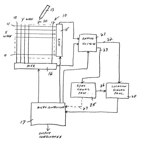
Fig. 1 is a block diagram illustrating features com~on to
many ~onventional d~gitizer tablet~, including those described in
the referenced patents and patent application. Those t~blets
comprise a console unit 10 in whose surface is e~edded a two-
dimensional arrangement of X and Y grid systems compri~ing,
respectively, a plurality of parallel X wires 11 and orthogonal Y
wires 12. A cordless pointing device illustrated as a stylus is
shown at 13.
The stylus 13 typically would contain an oscillator con-
nected to an antenna powered by an internal battery. ~or an
electromagnetic (EM) type of digitizer, the antenna would typi-
cally be a coil at the stylus tip. For an electrostatic type of
digitizer, the antenna would be a conductive tip. Each of the
conductor sets would be connected to a multiplexer 15, 16 in turn
connected to and controlled by a microcontroller 17. ~he outputs
from the multiplexers would conventionally be connected to loca-
tion signal processing circuitry 20.
In accordance with the invention, however, the multi-
plexers 15, 16 are connected to an analog switch 21 in turn con-
nected to and controlled by the microcontroller 17.
SCG.435.000.6 -5-
The analog ~witch 21 i8 e~Rentially a doubl~ pole, double
throw switch that ha~ two outputs 22, 23, th~ flr~t 22 o~ which
is connected to the location signal processor 20, and the ~econd
23 of which is connected to a 5ync signal processor 25. The out-
put of the latter can be connected as shown by the solid line 26
to lthe location signal processor 20, or as shown by the dashed
line 27 to the microcontroller 17. The output of the location
signal processor i8 fed to the ~icrocontroller 17 which ulti~ate-
ly outputs the X-Y coordinates of the stylus 13.
In operation, the user activates the stylus 13 when
over the console unit 10 generating a series of pulsed waves 30,
which induce signals in both the X and Y conductor wires ex-
tending underneath or in the vicinity of the stylus radiator.
The microcontroller 17 is programmed to send control signals to
the two multiplexers 15, 16 and analog switches 21 to do the fol-
lowing:
1. During one time interval, the X wires 11 are scanned
in a particular order and the induced signals forwarded to the
location signal processor 20;
2. While the X wires are scanned, the signals induced in
the Y wires, singly or ~ointly, are forwarded to the sync signal
processor 25. The latter occur at the same time that the loca-
tion signals are generated. Hence, there now exists a signal
which is properly timed with respect to the location signals that
can be used as described in the referenced patents and appl~ca-
tion as the required sync signal;
SCG.435.000.6 -6-
2. ~
3. When the X wire ~canning is co~pleted, during another
time interval, the Y wires 12 are scanned, the analo~ switch 21
being switched to now feed the Y location signals to the location
signal processor 21;
4. Si~ultaneously, the signals induced on the X wires 11
are forwarded to the sync signal processor 25.
Thus, without the addition of additional or auxiliary
grids, one axis of the tablet is used as a source for the sync
signal when the other axis is used for cursor location, with
their roles being reversed to obtain the second cursor coor-
dinate.
Fig. 2 illustrates some details of representative cir-
cuitry that can be used, most of which are well known to those
skilled in this art and need not be described in any detail. The
multiplexers 15, 16 are shown as 4051 chips, and the analog
switch 21 as a 4053 chip. The control signals from the micro-
controller 17 are not shown.
The signal processors for the sync and location signals
as shown are illustrated with conventional OP AMPS 31, 32, 33,
34, 35. The block 36 represents another 4053 analog switch
which, again controlled by the microcontroller which i~ not
shown, samples the location signals at its positive and negative
peaks for improved noise immunity. The signals are then passed
on to the usual AJD convertors and processed in the normal way to
produce the location information.
SCG.435.000.~ -7-
-
-,
~ L1~ ~
There are various ways in which the fiync conductor~,
i.e., the conductors from which the sync ~ignals are obtained,
can be chosen, elaborated on later in connertion with Figs. 6-8.
If the signal levels are sufficiently high, th~n any one grid
con~ductor can be used to provide the Rync s~gnal. Alternatively,
all of the grid conductors can be connected together by the mul-
tiplexer and switches --taking into account inverting polarities
where the signals are reversed-- to provide a reinforce~ higher
siqnal level. or, a group of such conductors, s~aller than the
total number, can be used to supply the sync signal.
Fig~ 3 shows a modified circuit which allows for ~witch-
ing to another conductor should the signal level fall below a
threshold value. The circuit is similar to the upper branch ~5
of the circuit shown in Fig. 2, showing in this case the
amplifier 33 as a block just before outputting the sync signal to
the microcontroller 17 or processor. In this modification, the
signal is tapped off to a third branch 40, where it is fed to a
conventional rectifier and filter section 41, resulting in a D.C.
level proportional to the amplitude as well as to the phase of
th~ incoming sync signal. This D.C. level is then fed to an A/D
converter 42 producing a digital value representative of the D.C.
level. This digital value can be compared 43 against a
predetermined threshold level. The results would be forwarded to
the processor 17. The latter is programmed to control the MUX
selecting the sync conductor such that, ~o long as the D.C. level
remains above the threshold, the same sync conductor or con-
SCG.435.000.6 -8~
.
' , ,, ' . ' : '
.. :
'~' "' ' " ' ~ ~ '
,:
ductors is used to supply the ~ync signal. Should the D.C. level
fall below the threshold, the processor would be programmed to
d~rect the MUX to 6elect another sync conductor or conductorq un-
til the qync signal level has been raised to an acceptable value.
The generated sync aignal, delayed if necessary, 1B used
as previously described to determine the proper time to scan the
X or Y wires, or for control of the S/H circuitry, or for any
other purpose where it i6 necessary to coordinate the cur~or
pulses with the signal processing.
Fig. 4 ~hows one way of using the sync signal for syn-
chronous demodulation o~ the cursor position signals. The wire
~elect and sync select blocks 50, 51 correspond to the ~nX's 15
and 16 of Fig. 1. The location signal i8 processed in the upper
branch 53 and inputted to the synchronous demodulator 54. The
sync signal is processed in the lower branch 55 and inputted to
the synchronous demodulator 54 which, as described in the
commonly-assigned cases, is used to sample the analog location
signal at the optimum time to maximize the S/N ratio. The output
at line 52 will be a D.C. level indicative of the amplitude and
phase of the location signal induced in the selected grid line
relative to that of the sync 5ignal. The output via line 52 is
then processed by the usual A/D converter 56, and in turn the
resultant value fed to the ~P 17, which, after the usual process-
ing outputs 57 the coordinate. The ~P 17 also supplies via line
58 the wire select signal to the MUX SO for the next scan of one
of the grids, and a wire select signal via line 59 to select
SCG.435.000.6 -9-
which grid llne or lines o~ the other grid will be used to supply
the sync signal.
Fig. 5 shows one form of implementation of the Fig. 4
block diagram, which is similar to that of Fig. 2, the ~ame
reference numerals being used for similar components. ~he 8ig-
nals induced in conductors of the X and Y grids are selected by
the respective MUXs 15 and 16, pre-amplified, an~ ~upplied to an
analog switch 21 controlled by signals from the proce sor (shown
by the block 60) such that when the Ax signal from the X grid is
used for location determination via branch 61 and low-pass filter
62, to be forward to the A/D converter, the By signal from the Y
grid i8 used via branch 66 to control analog switch 64 to
determine when the location signal should be sampled. Converse-
ly, when the Ay signal from the Y grid is used for the location
signal, the sync signal Bx is chosen from the X grid.
Fig. 6 illustrates a preferred way of selecting grid con-
ductors for location and sync signals using a signal waveform
which represents an integration of sample signals obtained from a
typical prior art EM digitizer. The Y axis of the graph
represents signal amplitude on a conductor (N), where the con-
ductor locations are represented in the waveform by X5 labelled
W3..W10. As is known, where the waveform crosses the time axis
is typically used to compute the cursor location. Hence, the
signals 70 from wires W6 and W7 are typically used for cursor
location. For maximizing noise immunity, strong signals are
SCG.435.000.6 -10-
' ' ",: " "
..
3 ~
desired. Hence, the 8ignal8 induced on conductor~ W4 or W5, or
both, are preferably used for deriving the sync signals.
Fig. 8 illustrates this modification, with the block 80
representJSng conventional tablet grid conductor or grid line se-
lect:ion circuitry for selecting the appropriate grid line during
the scanning process to derive the location signal, and block 81
representing a conventional selection circuit fox one or more
other grid lines for the sync signal, all under the control of a
microcontroller 82. This circuitry allows the grid lines 84 con-
nected to the location selector 80 to be, say, the X or Y grid,
when the grid lines 85 connected to the sync selector 81 are fro~
the other grid, namely Y or X, in a two grid system. But the
same circuitry can be used in a one-grid system, wherein the grid
lines 84 and 85 are part of the same grid, but are different, as
explained above. Moreover, the same circuitry can be used to
select two of the lines, such as represented by W4 and W5 in Fig.
6, and add their 5ignals to further increase signal strength.
Fig. 7 shows a typical response curve to illustrate a
further variation. If the signals induced on conductors 4 or 7
are typically u6ed ~ecause they provide the largest amplitude
signals, circuitry can readily be provided as illustrated
schematically in Fig. 8 to invert the phase 73 of one of the sig-
nals, and then add them together 74 to provide the sync signal.
This would improve the signal to noise ratio by 50 percent.
Moreover, once either of the peaks in Fig. 7 is initially
identified, tracking of the sync conductors remains constant.
SCG.435.000.6
',
That is to say, the conductor~ 4 ~nd 7, it will b~ noted ln thls
inst:ance, are separated by two conductors 5 and 6. It turns out
tha1: for ~ny system, regardless of position in the tablet, there
will always be the same conductor separation between the con-
ducl_ors with the largest signals. Hence this would simplify the
tracking of the selection circuit connections which are selecting
two conductors for the sync signals, illustrated at 86 in Fig. 8,
and should also ~id in providing, if desired, faster tr~ck move-
ments.
Fig. 8 also shows a conventional store 87 used to store
grid line signal values connected to a conventional peak detector
88 for identifying the conductors W4 and W5 in Fig. 6, or 4 and 7
in Fig. 7.
Reference is made to the referenced patents whose con-
tents are incorporated herein by reference, for more details if
needed on processing of the location and sync signal~ to
determine the X-Y coordinates of the pointing device.
While the invention has been described and illustrated in
connection with preferred embodiments, many variations and modi-
fications as will be evident to those skilled in this art may be
made therein without departing from the spirit of the invention,
and the invention as set forth in the appended claims is thus not
to be limited to the precise details of construction set forth
above as such variations and modifications are intended to be in-
cluded within the scope of the appended claims.
SCG.435.000.6 -12-