Note: Descriptions are shown in the official language in which they were submitted.
W092/0299~ 2 0 ~ ~ 9 7 7 PCT/US91/05316
DESCRIPTION
eciDrocal Mode Saw Correlator Method and Ap~aratus
BACKGROUND OF THE INVENTION
This invention relates to spread-spectrum communica-
tions, and more particularly to a spread-spectrum signal
processing technique through the use of a single phase
shift encoded tapped-delay line surface-acousticwave cor-
relator (SAWC) to demodulate multiple phase shift keyed
(PSK) codes.
The effects of surface-acoustic waves applied to a
piezoelectric material to convert electrical energy to
acoustic energy and ~ice versa for analog signal process-
ing purposes have been known and practiced in the prior
art for many years. This process, as applied to phase
coded SA~ correlators, cc~sists, in its mcst basic form,
of an input transducer and a phase coded tapped-delay line
matched to a phase shift encoded carrier. In general,
this operation is carried out by applying an electrical
signal to a transducer which consists of a sequence of
metallized interdigital finger pairs deposited on the
surface of a piezoelectric material. The transducer con-
verts this electrical signal to an acoustic wave whichpropagates down the surface of the substrate to the
tapped-delay line. Acoustic energy is converted to elec-
trical energy at the metallized delay-line taps. When the
phase encoded wave matc~es the phase configuration of the
2~ delay line taps, the electrical signals are added in phase
with each other, and a correlation signal, which provides
a signal to noise improvement, is generated and coupled to
other electronic circuits through the busses of the
tapped-delay line. Multiple correlations may be accom-
plished by placing separately encoded tapped-delay lines
in parallel on the same substrate. Distinct correlation
pulses will then occur upon application of matched phase
shift encoded signals at the transducer input.
W092/02997 2 ~ 7 7 PCT/US91/05316
The reciprocal properties of SAW devices allow for
this process to take place in reverse, where the tapped
delay line is excited by a phase coded electrical signal,
and a correlation signal will occur at the output of the
transducer. These reciprocal properties have been dis-
cussed for many years in literature and conferences.
Certain kinds of devices and signal formats have shown
more promise in this area than others. In 1973
J. Burnsweig of Hughes Corp. published a paper detailing
the use of linear FM pulse compression matched filters
operating in reciprocal manner ("Ranging and Data Trans-
mission Using Digital Encoded FM Chirp Surface Acoustic
Wave Filters", IEEE Transactions in Microwave Theory, Vol.
MTT-21, pp 272-279, April 1973). This approach involves
exciting the long tapped-delay line with the linear FM
encoded signal and utilizing t~e transducers, located a
certain distance away from each end of the delay line, as
the elements that coherently sum the waveform segments to
produce a compressed pulse. The reciprocal approach with
the linear FM chirp waveform was utilized to differentiate
between a "one" bit and a "zero" bit for satellite
ranging/data transmission applications.
While one and zero bit differentiation has been
applied toward a number of phase shift keyed (PSX) wave-
forms, most of these approaches appear to involve someform of acoustoelectric convolver and a hybrid network.
The simpler approach presented in this invention employs
a S~W BPSK matched filter configuration with two trans-
ducers located near the ends of a phase co~ed tapped-
delay line. As briefly described above, the two trans-
ducers are typically utilized as inputs either to assist
in generating the BPSK sequence or serve as the input for
the 8PSX encoded waveform, and the tapped-delay line
serves as the summing network to generate the correlation
peak. The reciprocal approach involves the use of the SAW
tapped-delay line as the input structure for a one bit
code and a reciprocal code representing the zero bit.
W092/02997 2 0 8 ~ ~ 7 ~ PCT/US91/0~316
Coherent summation o f the BPSK sequence can be sensed, at
a minimum within a chip width from one edge of the tapped-
delay line. The summation can be sensed by an appropriate
transducer structure that has dimensions corresponding to
one chipwidth along with having the correct inte~digital
finger spacing for the center frequency.
OBJECTS AND SUMMARY OF TH INVENTION
An o~ject of the invention is to provide a method for
demodulating multiple data bits from a phase code sequence
with a single tapped-delay-line surface-acoustic-wave
correlator.
Another object of the invention is to provide a
spread-spectrum receiver requiring no reference code
synchronization.
A further object of the invention is to provide
spread-spectrum demodulation through the use of single
tapped-delay-line SAW correlators which may be manufac-
tured with highly distinctive codes.
Another object of the invention is to provide a
~0 spread-spectrum demodulator which provides a lower band-
width to processing gain ratio and more code variability
than a linear FM chirp system. The BPSK encoded sequence
s more rGbust with respect to bandwidth narrowing and
some manufacturing tolerance variations compared with the
linear FM chirp waveform.
According to the present invention, as embodied and
broadly described herein, a system using a surface-
acoustic-wave correlator for decoding a spread-spectrum
signal having a data signal modulated with a plurality of
chip sequences and reciprocal-chip sequences is provided
comprising communications channel, data-sequence-generat-
ing means, chip-sequence-generating means, chip-sequence-
controlling means, signal means, carrier-modulating means,
power means, front-end means, tapped-delay-line means and
decision means. The data-sequence-generating means, chip-
sequence-generating means, chip-sequence-controlling
W092/02997 2 3 ~ 3 ~ 7 7 PCT/US91/05316 ~
means, signal means, carrier-modulating means, po~er
means, front-end means, tapped-delay-line means and deci-
sion means may be embodied as a data device, a code gen-
erator, a chip-sequence controller, a signal source, a
product device, a power device, a receiver-front end, a
tapped-delay line and a decision/detector circuit,
respecti~ely.
The data device generates a data-bit sequence having
first bits and second bits. The code generator repeti-
tively generates a chip sequence having a plurality offirst chips and second chips. The chip-sequence con-
troller outputs the chip sequence in response to each
first bit, and outputs the reciprocal-chip sequence in
response to each second bit. By reciprocal-chip sequence
is meant a time reversed version of the chip sequence. The
signal source generates a carrier signal. The product
device generates the spread-spectrum signal by phase modu-
lating the carrier signal with the chip sequence and
reciprocal-chip sequence. The power device sends the
spread-spectrum signal over the communications channel,
and optionally helps to limit a power level of the spread-
spectrum signal to less than a predetermined-threshold
level at the tapped-delay line.
The receiver-front end receives the spread-spectrum
signal. The tapped-delay line has a first end and a
second end. The tapped-delay line also has a plurality of
taps defining a tapped-delay-line structure phase-matched
to the chip sequence. The tapped-delay line generates a
plurality of TDL-chip sequences and inverse-TDL-chip
sequences, in response to each of the plurality of first
TDL chips and second TDL chips embedded in the spread-
spectrum signal, respectively. A TDL chip is defined as
a segment of the carrier signal of length equivalent to a
period of each chip generated by the chip generator, with
a first TD~ chip having a first phase, and a second phase
of a second TDL chip shifted with reference to the first
phase.
W092/02997 PCT/US9~/05316
7 ~
A first transducer is coupled acoustically to the
first end of the tapped-delay line. The first transducer
correlates a first sequence of the plurality of TDL chips
and inverse-TDL chips generated by the tapped-delay line
and outputs a first correlation pulse, in response to the
spread-spectrum signal modulated by the chip sequence. A
second transducer is coupled acoustically to the second
end of the tapped-delay line. The second transducer cor-
relates a second sequence of the plurality of TDL chips
and inverse-TDL chips generated by the tapped-delay line
and outputs a second correlation pulse, in response to the
spread spectrum signal modulated by the reciprocal-chip
sequence.
A decision/detector circuit outputs the first bit and
the second bit in response to detecting the first correla-
tion pulse and the second correlation pulse, respectively.
Additional objects and advantages of the invention
will be set forth in part in the description which fol-
lows, and in part will be obvious from the description,
or may be learned by practice of the invention. The
objects and advantages -of the invention also may be
realized and attained by means of the instrumentalities
and combinations particularly pointed out in the appended
` claims.
.
BRIEF DESCRIPTION OF THE DRAWINGS
The accompanying drawings, which are incorporated in
and constitute a part of the specification, illustrate
preferred embodiments of the invention, and together with
the description serve to explain the principles of the
invention.
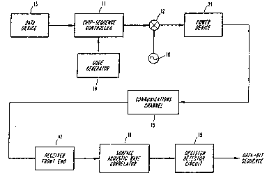
FIG. 1 illustrates a system using the reciprocal SAWC
in a spread-spectrum receiver according to the present
inventioni
FIG. 2A is an equivalent block diagram for a SAWC
BPSK matched filter showing a chip sequence generated by
a l-biti
W092/02997 PCT/US91tO5316 ~`
2~'8~7i~J
FIG. 2B shows the correlation values at the l-bit
transducer;
FIG. 2C shows the correlation values at the O-bit
transducer;
FIG. 3A is an equivalent block diagram for a SAWC
BPSK matched filter showing a chip sequence generated by
a O-bit:
FIG. 3B shows the correlation values at the O-bit
transducer: and
FIG. 3C shows the correlation values at the 1-bit
transducer.
DETAIL~D DESCRIPTION OF THE PREFERRED EMBODIM~NTS
The invention disclosed in this patent is related to
the inventions disclosed in U.S. patent application
entitled "Spread Spectrum Correlator", by Robert C. Dixon
and Jeffrey S. Vanderpool and having Serial No. 07/390,315
and Filing Date of August 7, l9B9, in U.S. patent applica-
tion entitled "Asymmetric Spread Spectrum Correlator" by
Robert C. Dixon and Jeffrey S. Vanderpool and having
Serial No. 07/389,914 and Filing Date of August 7, 1989,
and in U.S. pate~t application entitled "SAWC ~hase Detec-
tion Method and Apparatusl' by Robert C. Dixon and having
: Serial No. 07/556,147 and Filing Date of July 23, 1990,
. which are incorporated herein by reference.
~25Reference will now be made in detail to the present
preferred embodiments of the invention, examples of which
are illustrated in the accompanying drawings, wherein like
reference numerals indicate like elements throughout the
several views. The present invention includes a system
using a surface-acoustic-wave correlator for decoding a
spread-spectrum signal having a data signal modulated with
a plurality of chip sequences and reciprocal-chip
sequences. The system comprises a communications channel,
data-sequence-generating means, chip-sequence-generating
3S means, chip-sequence-controlling means, signal means,
W092/02997 PCT/US91/05316
2 ~ 7 ~
carrier-modulating means, power means, front-end means,
tapped-delay-line means and decision means.
As illustratively shown in FIG. 1, the data-
sequence-generating means, chip-sequence-generating means,
chip-sequence-controlling means, signal means, carrier-
modulating means, power means, front-end means, tapped-
delay-line means and decision means, by way of example,
may be embodied as a data device 13, a code generator 14,
a chip-sequence controller 11, an RF signal source 16, a
phase modulator 12, a power device 21, a receiver-front
-end 12, a surface-acoustic-wave correlator 18, and a
decision/detector circuit 19, respectlvely.
The chip-sequence controller 11 is coupled to the
data device 13 and the code generator 14. The phase
mo~ulator 12 is coupled to the RF signal source 16 and the
c~.ip-sequence controller 11. The power device 21 is
coupled to the product device 12.
The receiver-front end 17 is coupled to the communi-
cations channel 15. The surface-acoustic-wave correlator
` 20 18 is coupled to the receiver-front end 17. The decision/
detector circuit is coupled to the surface-acoustic-wave
correlator 18.
The data device 13 outputs a data-symbol sequence.
The data-symbol sequence usually includes in~ormation to
be communicated by the spread-spectrum signal. The data-
symbol sequence may have each data symbol represent two or
more data bits. In a binary case, the data-symbol
sequence has each data symbol represent one data bit, and
accordingly, the data-symbol sequence is known as a data-
bit sequence. The data-symbol sequence, for example, may
be a data-bit sequence having first bits and second bits,
which are the l-bit and 0-bit. As an example, the data
device 13 may be a computer terminal, a device which has
converted analog inputs such as voice, audio or video, to
data, or any other source where data are to be transmitted
from a transmitter to a receiver.
W092/02997 PCT/US91/0~316
` 2~9~
The code generator 14 repetitively generates a chip
sequence having a plurality of first chips and second
chips. The first chips and second chips are commonly
known as ls and Os. The repetitively generated chip
sequenc~ is known as the spreading sequence for generating
the spread-spectrum signal. In a preferred embodiment,
the chip seque~ce is a pseudo-noise (PN) code. The code
generator 14 may employ shift registers having appropriate
taps for generating the chip sequence.
For the binary case, the chip-sequence controller ll
outputs the chip sequence from the code generator 14 in
response to each first bit received from the data device
13, and outputs the reciprocal-chip sequence in response
to each second bit re~eived from the data de~ice 13.
Accordingly, the chip-sequence controller ll outputs a
concatenated plurality of chip seguences and reciprocal-
chip seguences, in response to a concatenated plurality of
first bits and second bits from data device 13.
For the binary case, the chip-sequence controller ll
causes a shift register containing the chip sequence to
shift in a forward direction for each first bit, and in
the reciprocal (opposite) direction for each second bit.
Thus, chip-sequence controller ll outputs a chip sequence
in the case of a data l-bit, and a reciprocal-chip
sequence for data 0-bit.
By reciprocal-chip sequence is meant a time reversed
version of the chip sequence. By way of example, if the
chip sequence is llO~Ol, then the reciprocal-chip sequence
is lOlOll. Preferably, a complete sequence o~ the repeti-
tively generated chip sequence or reciprocal-chip seguence
is outputted from the chip-sequence controller ll for each
data symbol. A chip sequence optionally may be generated
coherently with each data symbol of the data-symbol
sequence, and each data symbol determines whether a chip
sequence or its reciprocal is generated.
The signal source 16 generates a carrier signal. The
term "carrier signal" is defined herein to be any signal
W092/02997 PCT/US91/05316
2B~3~
at an RF, intermediate frequency (IF), or other frequency
at which the surface-acoustic-wave correlator 18 operates.
The center frequency of the carrier signal is matched to
the surface-acoustic-wave correlator 18 used at the
receiver.
The carrier-modulating means is coupled to the chip-
sequence-controlling means and the signal source 16, and
may be embodied as a product device or, as illustrated in
FIG. 1, a phase modulator 12. The phase modulator 12
generates the spread-spectrum signal by phase modulating
the carrier signal from the signal source 16 with the
plurality of chip sequences and reciprocal-chip sequences
from the chip-sequence controller 11, causing phase shifts
in the carrier signal corresponding to each state transi-
tion of the chip sequence. ~he spread-spectrum signal is
the carrier signal modulated with the output from the
chip-sequence controller 11. The phase modulator 12 out-
puts the spread-spectrum signal to the power device 21.
The power device 21 sends the spread-spectrum signal
over the communications channel 15, and limits a power
level of the spread-spectrum signal to less than a pre-
determined-threshold level at the input to the surface-
acoustic-wave correlator 18. The power device 21 is
optional, and includes any power amplifier and/or power
limiter. Typically, the power device 21 is coupled to a
communications channel from the surface-acoustic-wave
correlator 18. The transmitter power is adjusted to help
maintain the power level at the input to the surface-
acoustic-wave correlator 18 to below a predetermined-
threshold level which prevents the surface-acoustic-wave
correlator 18 from operating in a non-linear range. In
some commercially available devices, the predetermined-
threshold level has been found to be less than 20 dBm.
The communications channel 15 may be any medium where
the spread-spectrum signal may propagate or travel.
The receiver-front end 17 receives the spread-
spectrum signal from the communications channel 15. The
W092/02997 PCT/US91/05316 ~
2~8~
receiver-front 17 end includes any antenna, amplifier
and/or impedance matching circuitry coupling the surface-
acoustic-wave correlator 18 to the communications
channel 15.
The present invention includes a phase coded surface-
acoustic-wa~e correlator 18 for demodulating a received
spread-spectrum signal. The surface-acoustic-wave cor-
relator 18 comprises tapped-delay-line means, first
transducer means and second transducer means. As illus-
tratively shown in FIGS. 2A and 3A, the tapped-delay-line
means, first transducer means and second transducer means
may be embodied as tapped-delay line 30, first transducer
36, and second ~ransducer 37. The spread-spectrum signal
has a data signal embedded in a carrier signal by phase
modulating the carrier signal with a chip sequence and a
reciprocal-chip sequence, as previously described. The
received spread-spectrum signal is applied to the tapped-
delay-line bus, which serves as the surface-acoustic-wave
correlator 18 input. The tapped-delay line bus converts
the electrical signal received to an acoustic signal.
When a phase-matched-chip sequence is received at the
surface-acoustic wave correlator 18, an output transducer
will output a correlation pulse, which is applied to the
detection means, which may be embodied as an amplitude
and/or phase detector 19.
In a tapped-delay line, as the electrical signal is
converted to acoustical energy, an acoustic wave propa-
gates on the surface of a substrate, with each chip width
section of the wave adding in or out of phase with the
delay line fingers. When the acoustic waves reach the
output transducers at each end of the tapped-delay line,
the phase components of the wave are summed to create a
correlation pulse whose amplitude is in direct proportion
to the number of pha~e matches of the delay line. The
output transducers convert this acoustic energy to elec-
trical energy and output the correlation pulse in the
form of an amplitude modulated RF signal of frequency
W092/02997 2 ~ ~ g 9 ~ 7 PCT/US~1/05316
11
equivalent to the center frequency of the surface-
acoustic-wave correlator 18 and the received spread-
spectrum signal.
More particularly, as shown in FIGS. 2A and 3A, the
tapped-delay-line 25 has a plurality of taps defining a
- tapped-delay-line structure. In the exemplary arrangement
shown, the tapped-delay line 30 has five taps 31, 32, 33,
34, 35. The tapped-delay-line structure has the taps
adjusted to provide a phase match with a received spread-
spectrum signal modulated by the chip sequence or
reciprocal-chip sequence.
The tapped-delay line 30 has a first end and a second
end. The first transducer 36 i5 acoustically coupled to
tne first end of the tapped-delay line 30. The second
transducer 37 is aco~stically coupled to the second end of
the tapped-delay line 30. The tapped-delay line 30 gener-
ates a plurality of TDL-chip sequences and inverse-TDL-
chip sequences, in response to each chip of the plurality
of first chips and second chips embedded in the spread-
spectrum signal, respectively.
FIGS. 2A, 2B, and 2C illustrate the case for a
received spread-spectrum signal being a l-bit, which is
represented ~y the chip sequence lllOl. The received
spread-spectrum signal is applied to the tapped-delay-
line bus, which serves as the input to the tapped-delay
line 30. Each 1-chip of the chip sequence 11101 generates
in the tapped-delay line a tapped-delay-line-chip sequence
(TDL-chip sequence), lilOl, and each O-chip generates in
the tapped-delay line an inverse-TDL-chip sequence, OO010.
The generation of each TDL-chip sequence and inverse-T~-
chip sequence is delayed in time by the time equivalent of
one chip. FIG. 2B shows a group of TDL-chip sequences and
an inverse-TDL-chip sequences as they propagate as acous-
tic waves toward the first end of the tapped-delay line
30. The group shown in FIG.-2B is in response to the chip
sequence 11101, whic~ represents the l-bit. FIG. 2B shows
the output 61 of the first transducer 36, illustrated as
W092/02997 2 ~ ~ 8 ~ 7 ~ PCT/US91/0~316 ~`
12
a l-bit transducer, which is the su~ of the chips at any
point in time. The l-chips add in phase with the TDL
structure and are given a value of +l and the 0-chips add
out-of-phase with the TDL structure and are given a value
of -l. The output 61 shows that the firs~ transducer 36
generates a maximum value of 5, and accordingly the first
correlation pulse when the total of the output 61
reaches 5.
FIG. 2C shows a group of TDL-chip sequences and an
inverse-TDL-chip sequence as they propagate as acoustic
waves toward the second end of the tapped-delay line 30.
The group shown in FIG. 2C is in response to the chip
sequence lllOl, which represents the l-bit. The output 51
of the second transducer 37, illustrated as a 0-bit trans-
ducer, is the sum of the chips at any point in time. Thel-chips add in-phase with the TDL structure and are given
a value of +l and the 0-chips add out-of-phase with the
TDL structure and are given a value of -l~ The output 51
shows that the se~ond transducer 37 does not generate the
maximum level, since the levels are below a maximum value.
The decision/detector circuitry 19 detects which out-
put of the first transducer 36 and second transducer 37
produced the maximum value, and thereby outputs a l-bit if
the maximum value is from the first transducer 36.
FIGS. 3A, 3B, and 3C illustrate the case for a
received spread-spectrum signal being a 0-bit, which is
represented by the reciprocal-chip sequence lOlll. The
received spread-spectrum signal is applied to the tapped-
delay-line bus, which serves as the input to the tapped-
delay line 30. Each l-chip of the chip sequence lOlll
generates a tapped-delay-line-chip sequence (TDL-chip
sequence), lllOl, and each 0-chip generates an inverse-
TDL-chip sequence, OOOlO. The generation of each TDL-
chip sequence and inverse-TDL-chip sequence is delayed in
time by the time equivalent of one chip. FIG. 3B shows a
group of TDL-chip sequences and an inverse-TDL-chip
sequence as they propagate as acoustic waves toward the
WOg2/02997 PCT/US9~/0~316
2~3~77
second end of the tapped-delay line 30. The group shown
in FIG. 3B is in response to the reciprocal-c~ip sequence
10111, which represents the 0-bit. The output 51 of the
second transducer 37 is the sum of the chips at any point
5 in time. The l-chips add as a ~l and the 0-chips add as
a -1, as stated previously. The output 51 shows that the
second transducer 37 generates a maximum level of 5, and
accordingly the second correlation pulse when the total of
the output 51 reaches 5.
FIG. 3C shows a group of TDL-chip sequences and an
inverse-TDL-chip sequence as they propagate as acoustic
waves toward the first end of the tapped-delay line 30.
The group shown in FIG. 3C is in response to the
reciprocal-chip sequence 10111, which represents the
0-bit. The output 61 of the first transducer 36 is the
sum of the chips at any point in time. The l-chips add as
a +l and the 0-chips add as a -1, as stated previously.
The output 61 shows that the first transducer 36 does not
generate the maximum value, since the values are below the
maximum value.
The tecision/detector circuitry 19 detects which out-
put of the first transducer 36 and second transducer 37
produces the maximum value, and thereby outputs a 0-bit if
the ~aximum value is from the second transducer 37.
Accordingly, the first transducer 36 correlates a
first group of the plurality of TDL-chip sequences and
inverse-TDL-chip seque~ces generated by the tapped-delay
line 3~ and outputs a first correlation pulse, in response
to the spread-spectrum signal modulated by the chip
sequence. The first transducer 36 at the first end of the
tapped-delay line 30 produces a first correlation pulse
representing a data 1-bit, in response to the received
spread-spectrum signal modulated with the chip sequence.
Similarly, the second transducer 37 correlates a second
gro~lp of the plurality of TDL-chip sequences and inverse-
TDL-chip sequences generated by the tapped-delay line 30
and outputs a second correlation pulse, in response to the
W092/02997 ; 2 ~ 8 3 ~ ~ 7 PCT/US91/05316
spread-spectrum signal modulated by the reciprocal-chip
sequence. The second transducer 37 at the second end of
the tapped-delay line produces a second correlation pulse
representing a data 0-bit in response to the received
spread-spectrum signal modulated with the reciprocal-chip
sequence.
A decision/detector circuit l9 outputs the first bit
and the second bit in response to detecting ~he ~irst
correlation pulse and the second correlation pulse at the
outputs of the first transducer 36 and second transducer
~ 37, respectively.
The present invention further includes a method using
a surface-acoustic-wave correlator having a tapped-delay
line for encoding a spread-spectrum signal having a data
signal modulated with a plurality of chip sequences and a
reciprocal-chip sequences. The method comprises the steps
of: generating a plurality of TDL-chip sequences and
inverse-TDL-chip sequences with the tapped-delay line in
response to a plurality of first chips and second chips
embedded in the spread-spectrum signal matching the taps
of the tapped-delay line; correlating a first group of the
plurality of TDL-chip sequences and inverse-TDL-chip
sequences generated by the tapped-delay line: outputting
a first correlation pulse from a first transducer in
response to the spread-spectrum signal being modulated ~y
the chip sequence: correlating a second group of the
plurality of TDL-chip sequences and inverse-TDL-chip
sequences generated by the tapped-delay-line; outputting
a second correlation pulse from the second transducer in
response to the spread-spectrum signal being modulated by
the reciprocal-chip sequence; and outputting from a deci-
sion circuit the first bit and the second bit in response
to the first correlation pulse and the second correlation
pulse being outputted from the first transducer and the
second transducer, respectively.
It will be apparent to those skilled in the art that
various modifications can be made to the system using a
W092/02997 PCT/US91/05316
2~3~77
surface-acoustic-wave correlator or other analog corre-
lators, including but not limited to charged-coupled
devices, for decoding a spread-spectrum signal o~ the
instant invention with out departing from the scope or
spirit of the invention, and it is intended that the
present invention cover modifications and variations of
the system using the surface-acoustic-wave correlator
provided they ~ome in the scope of the appended claims and
their equivalence. Such modifications and variations
include, but are not limited to, applying the surface-
- acoustic-wave correlator to communications systems employ-
ing other type of phase modulation such as QPSK and M-ary
PSK.