Note: Descriptions are shown in the official language in which they were submitted.
COMPACT FLUORESCENT LAMP SYSTEM
sAcKGRouND-oF THE INVENTION
This invention relates to compact low-pressure gas
discharge lamps and more particularly to a system including
a lamp assembly and a power supply for the lamp assembly.
The invention is especially adapted to providing practic~l
dimming capabilities for compact fluorescent lamps.
Compact fluorescent lamps have long been known for
their high luminous efficiency and have made great strides
in replacing relatively inefficient incandescent bulbs.
Because fluorescent lamps are typically provided in
elongated tubular form, efforts have been made to
reconfigure their light transmitting enclosures into a
series of short parallel tubes or stubs. Prior attempts
have ~oaused on reforming the light transmltting enclosure
of a single gas discharge lamp into a serpentine
con~lguration, such as illustrated in United States Patent
4,347,460, or into a series of cross coupled tubes as
illustrated in United States Patent 4,545,774. Such prior
attempts have resulted in lamps that could be manufactured
only by extremely complex manufacturing processees.
There has been a long felt yet unmet need for
practical, dimming capabilities for compact fluorescent
lamps. While various schemes have been proposed, none of
them have been commercially acceptable. This is believed to
be a result of the unusual and demanding operating
characteristics of such compact fluorescent lamps. Dimming
techniques that are suitable for incandescent lamps are
incompatible with fluorescent lamp circuits.
Because the primary benefit of compact fluorescent
lamps is envisioned to be in the replacement of incandescent
- - - - . ~
lamps, compact fluorescent lamp adapters have been used for
the purposes of adapting conventional incandescent lamp
fixtures for use with compact fluorescent lamps. This not
only avoids unnecessary expense in equipment replacement but
allows the substitution to be easily performed by th~ end
user. Such adapters have not been without their drawbacks.
Compact fluorescent lamps are heat sensitive, and the waste
heat produced by the lamp ballast circuit tends to reduce
lamp longevity when combined in the same assembly with the
fluorescent lamp.
SUMMARY OF THE INVENTION
The present invention provides a unique compact
low-pres6ure ga~ discharge lamp assembly having a base and a
plurality of low-pres~ure gas discharge light generating
elements mounted to the base. Each o~ the light generating
elements are capable of being individually energized.
Supply means are provided with the base for conducting
electrical energy to each of the light generating elements.
This allows conventional U-shaped and H-shaped compact
fluorescent lamps, for which manufacturing capacity if
readily available, to be assembled into a lamp assembly
without undue manufacturing complexity. Additionally, if a
light generating element fails, the remaining elements of
the lamp assembly continue to generate light so that the
lamp assembly may continue to be useful while awaiting
replacement.
According to another aspect of the invention, a
ballast circuit is provided that is adapted to supplying
electrical energy to a selective number of such light
generating elements of the lamp assembly. A switch assembly
may be provided that is adapted to connecting the ballast
circuit selectively to particular ones of the light
generating elements. This provides dimming capabilities to
the system by providing selective operation of different
numbers of light emitting elements.
~ ccording to another aspect, the present invention
:Ls especially adapted to providing such dimming capabilities
to conventional incandescent lamp fixtures having a
three-way switch and socket. Such fixtures are provided for
use with incandescent lamps having a high intensity filament
and a low intensity filament connected with separate
contacts in the lamp base. The three-way switch provides
energy to the low intensity filament for a low-light output,
to the high intensity filament for a medium-light output and
to both filaments for a high-light output. According to
this aspect of the invention, a lamp assembly having a
plurality of compact gas discharge light generating elements
that are capablo o~ being individually energized, are
conneated with the three-way switch such that one of the
light generating elements is energized in a first switch
position, two other light generating elements are energized
in a medium switch position and all light generating
elements are energized in a third, or high, switch position.
This aspect of the invention i9 especially
advantageous because it provides dimming capabillty, not
previously available in a compact fluorescent light system,
utilizing readily available incandescent light ~ixtures. In
a disclosed embodiment, the ballast clrcuit is provided in a
module which may be plugged into a conventional wall outlet
and is adapted to receiving the plug of a conventional table
lamp. This provides dimming capabilities with the three-way
switch in a conventional tabl~ lamp with the ga5 discharge
- . . . - .
,, , -,
lamp assembly being threaded into the conventional three-way
socket of such table lamp. Advantageously, this aspect of
the invention further allows, for the first time, dimming
capabilitie~ of compact fluorescent lamps used in
permanently installed recessed lighting and track lighting
fixtures.
These and other objects, advantages and features
of this invention will become apparent upon review of the
following specification in conjunction with the drawings.
BRIEF DESCRIPTION OF THE DRAWINGS
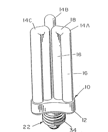
Fig. 1 is a Pront perspective view of a lamp
asæembly acaording to the invention;
Fig. 2 is a top plan view of the lamp assembly in
Fig. l;
Fig. 3 is a bottom plan view of the lamp assembly
in Fig. l;
Fig. 4 is a rear elevation of the lamp assembly in
Fig. 1 with a portion of the base removed to reveal internal
structure thereof;
Fig. 5 is an electrical schematic diagram of a
lamp system according to the invention;
Fig. 6 is the same view as Fig. 1 of an
alternative embodiment of a lamp assembly according to the
invention;
Fig. 7 is a perspective view of a lamp system
according to the invention: and
- Fig. 8 is a partial perspective view and partial
electrical schematic diagram of an alternative embodiment of
a lamp system according to the invention.
DESCRIPTION OF THE PREFERRED EMBODIMENT
Referring now specifically to the drawings, and
the illustrative embodiments depicted therein, a
low-pressure gas discharge lamp assembly 10 includes a base
12 and a plurality of individual low-pressure gas discharge
light emitting elements 14a-14c extending from base 12
(Figs. 1-3). Light emitting elements 14a-14c contain
mercury vapor at low-pressure with a small amount of inert
ga~ for generating ultraviolet energy to activate
fluorescent powders. Such lamps are commonly referred to as
compact fluorescent lamps. Light emitting elements 14 are
conventional U-shaped compact fluorescent lamps having a
pair of parallal shafts 16 joined together at a bite portion
18. Alternatively, light emitting elements 14' may be used
that are of a conventional H-shaped configuration include a
pair of tubes 16' joined with a stub 18' (Fig. 6).
Tubes 16 of all light emltting elements 14
terminate within base 12 (Fig. 4). Only one tube 16 for
each light emitting element 14 is shown in Fig. 4 ~or
clarity. Supply means for conducting electrical energy to
each of the light emitting elements 14a-14c, generally ~hown
at 20, includes a contact assembly 22 and a plurality of
inductive devices 24 interconnecting the contact assembly
wlth light emitting elements 14. An inductive device
24a-24c i8 eleatrically interconnected betwaen a contact
assembly 22 and cathodes 25a-25c of one tube 16 of each
light emitting element 14a-14c. Each cathode 25a-25c is
electrically series connected with a capacitor and the
re~pective cathodes 26a-26c of the other tube 16 of the same
liqht emitting element. Other electrodes 26a-26c are, in
turn, ~oined together and connected with a common contact 28
of contact assembly 22 as seen in Fig. 5. Contact assembly
.
" ,' ' ' ' ' ' ' ' '
22 includes a contact 30 to which inductive devices 24a and
24b are electrically connected and a contact 32 to which
inductive device 24c is electrically connected. In the
illustrative embodiment, contact assembly 22 is a
conventional three-way incandescent lamp base in which
contact 28 is electrically common with the metallic threads
34 of the screw-base and contacts 30 and 32 are concentric
contacts mounted at the end of contact assembly 22 axially
outward of threads 34. As will be set forth in more detail
below, when a suitable electrical potential is applied
acxoæs contacts 32 and 28, light emitting element 14c
connected with inductive device 24c will illuminate and emit
light. When a suitable electrical potential is applied
across contacts 30 and 28, light emitting element 14a
connected with inductive device 24a and light emitting
element 14b connected with inductive device 24b will
illuminate. When a suitable electrical potential is applied
across contacts 30 and 28 and across contacts 32 and 28, all
light emitting elements 14a-14c will illuminate and emit
light.
Lamp assembly 10 i8 supplied with electrical
energy in a lamp 6ystem 40 including a ballast circuit 42
and, preferably, a switch assembly 44 (Fig. 5). Ballast
circuit 42 includes a pair of input terminals 46, which are
illustrated as a conventional plug, ~or interconnection with
a high voltage AC power source, such as a house wall outlet.
Ballast circuit 42 produces an output across output contacts
48 and 50. Output contact 48 is connected with switch
assembly 44 which, in the illustrated embodiment, is a
conventional three-way switch having switch elements 52a,
52b, 52c and 52d that are separately, selectively actuated
by an actuator 54. Switch assembly 44 includes a first
output contact 56 that is electrically connectad with
contact 30 of lamp assembly 10 and a second output contact
58 that is electrically connected with contact 32 of lamp
assembly 10. As is conventional, all elements 52a-52d are
open when actuator 54 of switch assembly 44 is in an off
position. When actuator 54 is rotated to a first, or
low-light position, only switch element 52a closes. When
actuator 54 is rotated from the first to a second, or
medium-light output position, element 52a opens and element
52b closes. When actuator 54 is further rotated to a third,
or high-light output position, element 52b opens and
elements 52a and 52d close. In this manner, output 48 of
ballast circuit 42 i8 electrically connected with contact 30
o~ lamp as6embly 10 when actuator 54 i8 rotated to the first
low-light position in order to illuminate light emitting
element 14c. Ballast circuit output 48 is aonnected with
contaat 32 of lamp assembly 10, when actuator 54 is rotated
to a medium light position and, thereby, energizes light
emitting elements 14a and 14b but not 14c. Ballast circuit
output 48 is applied to both contacts 30 and 32 of lamp
assembly 10 when actuator 54 is rotated to a high output
position and, thereby, illuminates all light emitting
elements 14a-14c. As will be set forth in more detail
below, ballast circuit 42 in combination with lamp assembly
10 is adapted to supplying substantially a suitable current
to each light emitting elements 14a-14c irrespective of the
number of element~ that are interconnected by switch
assembly 14 with the ballast circuit.
In one form of the present invention, lamp system
40 includes a conventional incandescent lamp fixture 60
having a three-way switch and socket assembly 62 (Fig. 7).
:Cn lamp system 40 illustrated in Fig. 7, ballast circuit 42
is enclosed within a housing 64 with supply voltage contacts
46 extending from a wall of the housing 64. A molded
receptacle ~6 interconnected with housing 64 by a cable 68
:Lncludes output contacts 48 and 50 of the ballast circuit.
Xn this manner, the contacts 48 and 50 of the ballast
circuit are interconnected with switch 44 through the plug
and cord assembly 70 of lamp fixture 60. Accordingly,
conventional three-way lamp fixture 60 may be adapted to use
with lamp system 40 by inserting ballast circuit module 42
into a conventional wall outlet and interconnecting the plug
of cord 70 with receptacle 66. Lamp assembly 10 is
conveniently threaded into the three-way socket of switch
and socket assembly 62. As set forth in more detail above,
as actuator 54 is rotated from an off through low, medium
and high light output positions, a first light emitting
element 14a-14c i8 illuminated in the first position, two
light emitting elements 14a-14c are illuminated in the
medium position and all three light emitting elements
14a-14c are illuminated in the high light output position.
The present invention is additionally useful in
providing dimming capabilities for compack fluorescent lamps
in a recessed lamp system 14' (Fig. 8). Lamp system 40'
includes a recessed light fixture 72 having a conventional
three-way incandescent lamp socket 74. With light fixture
72 mounted to a ceiling surface 76, or the like, ~ocket 74
may be wired using conventional cable 78 with a wall-mounted
dimmer switch 44' and ballast circuit 42'. Ballaet circuit
42' may be combined in the same housing with dimmer switch
44' and be connected using conventional wiring techniques
with the 120/240 volt house power grid. Because the
interconnections from dimmer switch 44' to light fixture 74
requires two hot lines and one return, or ground, line,
conventional Romex cable, or the like, may be used. In this
manner, special cable avoided. The same principle may be
used to supply power to multiple lamp assemblies 10, all
wired in electrical parallel with each other on a
conventional track lighting track (not shown).
Ballast circuit 42 includes a full wave rectifier
bridge 78 that produces, from a 120 VAC source, a 160 DC
power ~ource at output 80 that i5 applied across a filter
capacitor 82 tFig. 5). Output 80 is applied through a bias
resistor 84 to a junction 86. Junction 86 is connected
through a break-over device, or diac 88 to a junction 90. A
resistor 92 extends between ~unction 90 and the gate 94 of a
swltching device 96. Junction 90 additionally connects with
a terminal of a transformer winding, designated TRA, whose
other terminal connects wlth a ~unction 98. Junction 98, in
turn, connects with a transformer winding TRP whose other
terminal 100 is connected through a capacitor 102 to output
contact 50.
Junction 98 additionally connects through opposite
polarity back-to-back zener diodes 104 and 106 to gate 94.
In the illustrated embodiment, switching device 96 is a
field effect transistor (FET) whose source i8 connected with
junction 98 and whose sink i5 connected with junction 108
which is, in turn, connected with output contact 48.
Junction 108 is undiroctionally isolated from ~unction 86 by
a dlode 110 and connects through opposite polarity
back-to-back zener diodes 112 and 114 with the gate 116 of a
switching device 118. Gate 116 is additionally connected
- . ,. : ::
~ ~i 3 ~ L ~ ~P
through a resistor 120 to one terminal of a transformer
~winding TRB whose othe.r terminal connects with junction 108.
In the illustrated embodiments, switching device 118 is a
FET whose source is connected with junction 108 and whose
sink is connected with output 80. Transformer windings TRA,
TRB and TRP are commonly wound on a ferrite core in a manner
that TRP is the primary winding and TRA and TRB are
secondary windings with TRA and TRB being wound in an
opposing plurality to each other, as indicated by the
polarity sym~ols in Fig. 5.
Bias circuit 42 operates as follows. Upon the
application of power thereto, the voltage at junction 86
will conduct a current to junction 90 when the break-over
voltage of diac 88 is exceeded. This current will be
applied to gate 94 causing switching device 96 to conduct.
This will pull output ~unction 108 low and cause a current
to pass through winding TRP. Additionally, a bias will be
applied to gate 116 of switching device 118 forcing it into
a nonconducting state. The result will be a current induced
through winding TRP of a direction tending to induce a
voltage across winding TRA of a polarity to force gate 94
low, turning off switching device 96 and inducing a voltage
across winding TRB of a polarity forcing gate 116 high,
driving switching device 118 into a conducting mode. This
causes the output voltage on junction 108 to switch to a
positive state and causes a reversal of the current through
primary winding TRP. The reversal of current through
winding TRP again switches switching device 96 into a
conducting state and switches switching device 118 into a
nonconducting state. The purpose of zener diodes 104, 106,
--10--
112 and 114 are to protect switching device 96 and 118 from
excesslve voltage peaks.
As three-way switch 44 changes the number of light
emitting elements 14 connected to bias circuit 42, the
frequency of the square-wave output signal on output
conductor 48 is varied as a result of the change in
capacitance produced by the different number of light
emitting elements which are capacitive devices. Capacitor
102 provides isolation between the electronic components of
ballast circuit 42 and light emitting element 14a-14c and
additionally serves to establish a power factor for the
circuit as close as possible to unity. The variation in the
frequency of the output signal on output contact 48, as a
result of switching the number of light emitting elements
connected in the circuit, tends to compensate for the change
in capacitanae from the change in the number of connected
elements in a mannsr that maintains a relatively constant
power factor. Thus, bias circuit 42 produces an
exceptionally efficient source of excitation for light
emitting elements 14 irrespective of the number of such
elements being connected to the bias circuit. Capacitors
~7a, 27b and 27c across the cathodes 25a-25c and 26a-26c,
rsspectively, provide "instant start" ignition of the light
emitting elements 14a-14c by providing current through the
cathodes to heat the cathodes to a state where ions are
emittad, in order to strike an arc. Instant start ignition
circuits are convantional in the art.
While values of components may vary depending upon
the power consumption of the particular light emitting
elements used, the following is representative of component
values that are useful in the illustrated embodiment:
,....... . , ~ ~
COMP~ONENT IDENTIFICATION NO.
Capacitor 82 47UF, electrolytic
Resistor 84 47X, ohms
Diac 88 27 volt break-over
device manufactured by
Diode, Inc., Model RB153
Switching Devices Model IRF730 FET
96 and 118
Diodes 104, 106 lN 47468A Zener
114 and 112
Inductive Devices 1300 microhenry,
24a, 24b and 24c Model IHA~1-01 by Dale
Electronics
Winding TRP 5.3 microhenry,
0.01 ohms (1 turn, 30
gage wire)
Winding TRA and TRB 594 microhenry,
0.17 ohms (20 turns,
33 gage wire)
Reei6tors 92, 120 120 ohms
In the illustrated embodiment, light emitting
elements 14 are type PL miniature fluorescent lamps of the
type manufactured by Osram, although other conventional lamp
configurations may be utilized, as illustrated in Fig. 6.
Although the invention was described with respect to three
light emitting elements 14, a greater or lesser number of
elements may be used. Additionally, various elements of the
illustrated embodiment may be useful in various
configurations. For example, lamp assembly 10 and ballast
circuit 42 may be advantageously used to provide exceptional
light output and an ability to continue to produce light,
notwith~tanding the failure of one or more of the light
emitting elements. These advantage6 may be obtained without
the use of switch assembly 44.
Accordingly, it is seen that the present invention
provides a unique lamp assembly and a lamp system using such
-12-
Lamp assembly. The system provides, for the ~irst time, a
practical dimming capability for compact fluorescent lamps
and does so in a manner that takes advantages of the
Eeatures of conventional incandescent lamp fixtures.
Specifically, dimming capabilities for compact fluorescent
:Lamps is provided by adapting a three-way lamp fixture, of
the incandescent variety by plugging an adapter element into
a conventional wall outlet with the incandescent lamp
fixture being plugged into the adapter element. Not only
does thi6 provide dimming capabilities, but the isolation of
the ballast circuit from the lamp as~embly avoids a
significant detriment to longevity of such compact
fluorsscent lamps, namely, deterioration as a result of the
heat generated by the ballast circuit. Because the ballast
circuit is physically removed from the lamp socket, its heat
doe~ not affect the lamp assembly. Furthermore, a ballast
circuit is disclosed which is exceptlonally efficient and,
accordingly, does not generate an excessive amount of waste
heat. The invention further provides, for the first time,
practical dimming capability for recessed lighting and track
lighting systems.
Changes in modifications in the specifically
described embodiments can be carried out without departing
from the principles of the invention, which is intended to
be limited only by the scope of the appended claims, it is
interpreted according to the principles of patent law
including tha doctrine of equivalents.
-13-
"' ' ' - ' `~ ~ "'' . ' ~