Note: Descriptions are shown in the official language in which they were submitted.
RCA 86,714
~~~~2J~.
A DEFLECTION CIRCUIT HAVING A
CONTROLLABLE SAWTOOTH GENERATOR
The invention relates to a sawtooth generator of a
deflection arrangement in a video apparatus.
Typically, a vertical sawtooth generator of a vertical
deflection circuit in a televisi_on_receiver_ utilizes a current
integrating capacitor that is charged.. from a source of a D.C.
current to produce a ramp, trace portion of an output sawtooth
signal synchronized to a vertical synchronizing signal. The trace
portion of the sawtooth signal controls a trace portion of a vertical
deflection current that produces vertical deflection in a cathode
ray tube (CRT).
The value of the capacitance of the capacitor may have
an appreciable effect on the amplitude of the sawtooth signal. A
change in, for example, the capacitance of the integrating capacitor
due to, for example, aging or temperature variation may tend to
vary the amplitude of the sawtooth signal.
U.S. Patent 4,686,432 entitled VERTICAL DEFLECTION
2 0 CIRCUIT FOR ELECTRON BEAMS IN PICTURE TUBE, in the names of
Berland et al., discloses an arrangement in which a pulse occurnng
at the center of vertical trace is used for sensing the difference
between the sawtooth signal and a reference voltage and for
controlling the current source in accordance with such difference.
2 5 The level of the sawtooth signal is established at the center of
vertical trace at a magnitude that is equal to that of the reference
level.
In order to control the amplitude of the sawtooth
signal accurately, it may be desirable to sense the aforementioned
3 0 difference between the sawtooth signal and the reference voltage
at an instant that is significantly closer to the end of vertical trace
than to the center. The length of the vertical period may be
different for standard and nonstandard synchronizing signals.
The limit as to how close to the end of vertical trace such sensing
3 5 can occur is determined by the minimum required period of the
vertical sawtooth signal for the range of values of the required
vertical period.
-z- ~d~~~~~ RcA gs,m4
A video display deflection apparatus, embodying an
aspect of the invention, includes a first capacitor. A current that
flows in the capacitor in a first direction is generated to produce a
first ramping portion of a sawtooth signal in the capacitor, during
a first portion of a period of the sawtooth signal, and in a direction
that is opposite to the first direction to produce a second ramping
portion of the sawtooth signal, during a second portion of the
period. The sawtooth signal is synchronized to a synchronizing
signal. The first ramping portion is established at a level that
1 0 corresponds to a first reference level. A timing control signal is
generated during the first ramping portion. The capacitor current
is controlled in a gain control feedback manner, in accordance
with a difference between the first ramping portion and the
second reference level. The difference is determined when the
timing control signal is generated. A length of an interval
between the first instant, when the first predetermined level is
established, and a second instant, when the timing control signal is
generated, is greater than one-half of a length of the first ramping
portion of the sawtooth signal. A first amplifier is responsive to
2 0 the sawtooth signal and coupled to a deflection winding for
generating a deflection current in the deflection winding that
varies in accordance with the sawtooth signal to form a raster on a
screen of a cathode ray tube.
The typical integrating capacitor of the vertical
2 5 sawtooth generator has a larger capacitance than cannot be
fabricated using integrated circuit (IC) fabrication technique. It
may be desirable to fabricate the integrating capacitor using the
IC fabrication technique.
In accordance with an aspect of the invention, a
3 0 current source that is controlled in a negative feedback manner is
applied to an integrating capacitor fabricated with the IC
fabrication technique to produce the sawtooth signal.
FIGURES 1 a, 1 b and 1 c illustrate, a vertical deflection
circuit, embodying an aspect of the invention; and
3 5 FIGURES 2a-2d illustrate idealized waveforms of the
arrangement of FIGURE 1.
FIGURES la, lb and lc illustrate, partially in block
diagram form, a vertical deflection circuit, embodying an aspect of
~~~~~~I
- 3 - RCA 86,714
the invention that includes a sawtooth generator 100. A
synchronizing signal SYNC produced by, for example, a video
detector of a television receiver, not shown, that processes a
television signal conforming to the NTSC standard, for example, is
coupled to a vertical timing generator 10. Generator 10 generates
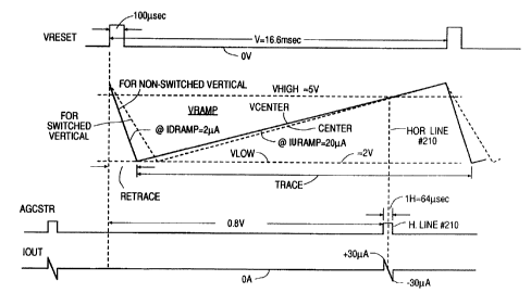
a vertical rate pulse signal VRESET, as shown in FIGURE 2a.
Similar symbols and numerals in FIGURES 1 a, 1 b, lc and 2a-2d
indicate similar items or functions.
Pulse signal VRESET of FIGURE la is coupled to a "set"
1 0 input of a Set-Reset flip-flop 12 causing flip-flop 12 to change
states. Consequently, an output Q of flip-flop 12 produces a
leading edge LE of an output control signal 112a. Leading edges of
signals VRESET and 112a occur at the end of a given vertical trace
interval and initiate vertical retrace. Signal 112a is coupled , to a
control terminal 13a of a current switch 13. Immediately after
leading edge LE, signal 112a causes switch 13 to couple a D.C.
current IDRAMP to a junction terminal 18a of an integrating
capacitor 14 that is fabricated using an integrating circuit (IC)
fabrication technique.
2 0 Current IDRAMP is produced in a voltage-to-current
(V/I) converter 15 that is controlled by a voltage VRSLOPE
produced in a digital-to-analog (D/A) converter 16. The digital
data input to D/A converter 16 is supplied via a bus BUS from a
microprocessor 17. Microprocessor 17 may additionally control
2 5 various adjustment functions, not shown, in the television receiver
such as S-shaping and East-West correction. A second end
terminal 18b of integrating capacitor 14 is coupled to an output of
an amplifier 18 where a sawtooth signal VRAMP is generated.
Current IDRAMP forms a retrace portion RETRACE of sawtooth
3 0 signal VRAMP of FIGURE 2b. Terminal 18a of capacitor 14 of
FIGURE 1 a is coupled to an inverting input terminal of amplifier
18 to form a current integrator.
Signal VRAMP of FIGURE la is also coupled to a
noninverting input terminal of a comparator 19 that senses the
3 5 level of signal VRAMP during portion RETRACE to determine an
end time of portion RETRACE of signal VRAMP. An inverting input
terminal of comparator 19 is coupled to a source of a D.C.
reference voltage VLOW that is generated in a manner discussed
- 4 - RCA 86,714
later on. An output terminal 19a of comparator 19 is coupled via
an "OR" gate 20 to a "reset" input R of flip-flop 12.
When, as a result of current IDRAMP, signal VRAMP
ramps down and attains a level that is equal to voltage VLOW,
comparator 19 produces an output signal that causes flip-flop 12
to change states and to produce, at output Q, a trailing edge TE of
signal 112a. Thereafter, current IDRAMP is decoupled from
capacitor 14 by switch 13.
A magnitude of current IDRAMP is programmable, in
accordance with the value of the digital data input to D/A
converter 16 for providing the required retrace slope or length of
portion RETRACE of signal VRAMP. For example, in an
arrangement similar to that of FIGURE la, intended for controlling
a switched vertical deflection circuit, not shown, V/I converter 15
may be programmed to produce current IDRAMP of a smaller
magnitude than in FIGURE 1 a. In this way, portion RETRACE is
lengthened, as shown in broken line in FIGURE 2b, relative to the
length of portion RETRACE used for controlling a non-switched
vertical deflection circuit such as shown in FIGURE lc. Thus, a
2 0 retrace portion RETRACE of signal VRAMP of FIGURE 2b can be
made adaptable for operation with either a switched or non-
switched vertical deflection circuit.
Provided that the pulse width of signal VRESET of
FIGURE la is shorter than the length of portion RETRACE of signal
2 5 VRAMP, the precise timings of the trailing edge of signal VRESET
is, advantageously, not critical. The advantage of not being critical
is that timing generator 10 that is required for processing both
nonstandard and standard sync signal SYNC can be simplified.
Nonstandard sync signal SYNC might be received from, for
3 0 example, a video tape recorder operating in a freeze-frame or still
picture mode.
A D.C. current IURAMP that is substantially smaller
than current IDRAMP is produced in a V/I converter 21. After
trailing edge TE of signal 112a, current IURAMP that is coupled to
3 5 terminal 18a of capacitor 14 charges capacitor 14 to produce a
ramping trace portion TRACE of sawtooth signal VRAMP of FIGURE
2b. The magnitude of current IURAMP of V/I converter 21 of
FIGURE 1 a is controlled in an automatic gain control (AGC)
- 5 - RCA 86,714
feedback loop by a voltage VAGC, developed across a capacitor 22.
Voltage VAGC controls converter 21 such that the more positive is
voltage VAGC, the smaller is current IURAMP. An AGC strobe
signal AGCSTR is coupled to a control terminal 24a of a switch 24.
S In accordance with an aspect of the invention, signal
AGCSTR is produced in vertical timings generator 10 close to the
end of vertical trace. Signal AGCSTR has a pulse width that is
equal to the length of, for example, a horizontal video line or 64
microseconds. During the occurrence of the pulse of signal
1 0 AGCSTR, a current IOUT, generated in a V/I converter 23, is
coupled via a switch 24 to capacitor 22. Outside of the occurrence
of the pulse of Signal AGCSTR, capacitor 22 maintains its voltage
approximately at a constant level to provide sample-and-hold
operation. The magnitude of current IOUT is controlled in
I S converter 23 is proportional to a difference between signal
VRAMP and a reference voltage VHIGH, that is produced in a
manner described later on.
During a given trace interval, should the magnitude of
signal VRAMP be smaller than voltage VHIGH when strobe signal
2 0 AGCSTR occurs, current IOUT would be positive and at a
magnitude that is proportional to the difference between voltage
VHIGH and signal VRAMP. Positive current IOUT causes a
decrease of voltage VAGC in capacitor 22. Consequently, in
subsequent vertical trace intervals, current IURAMP would be
2 5 larger and the rate of increase of signal VRAMP would be greater
than before in a manner to compensate for the aforementioned
tendency of signal VRAMP to be smaller than required.
Conversely, should the magnitude of signal VRAMP be
larger than voltage VHIGH, when the pulse of signal AGCSTR
3 0 occurs, current IURAMP, in the subsequent vertical trace
intervals, would be smaller. Thus, the AGC feedback loop causes
the magnitude of signal VRAMP to be at the same level of voltage
VHIGH, when strobe signal AGCSTR occurs. In steady state
operation, the polarity of current IOUT changes at the center of
3 5 the pulse of signal AGCSTR, as shown in FIGURE 2d.
Immediately after the circuit is energized, capacitor 22
is fully discharged. Capacitor 22 is coupled to voltage VCC.
Therefore, upon power turn-on, voltage VAGC is equal to voltage
~~d~~~~
- 6 - RCA 86,714
VCC and the amplitude of ramp signal VRAMP is at a minimum or
zero. Had capacitor 22 been coupled to ground, instead, the
amplitude of signal VRAMP at power turn-on might have been
excessive. Excessive amplitude of signal VRAMP could cause
excessive deflection current amplitude. The result could be that
the electron beam in CRT 49 could impinge on a neck of CRT 49
and damage CRT 49.
In accordance with an inventive feature, signal
AGCSTR is made to occur further from the center of vertical trace
portion TRACE and as close to the end of vertical trace as feasible.
In this way, the length of an interval between the instant when
the level of signal VRAMP is established to be equal to voltage
VLOW and the instant when signal AGCSTR is generated is, for
example, at the maximum feasible length. The upper limit as to
1 5 how late in the cycle of signal VRAMP, signal AGCSTR can occur, is
determined by the minimum required length of the vertical cycle
of signal VRAMP. Illustratively, signal AGCSTR is selected to occur
after an interval T, having a length of 80% of the nominal vertical
period V, has elapsed from the trailing edge TE of signal 112a, as
2 0 shown in FIGURE 2c.
A time CENTER occurs at the center of portion TRACE.
At a time that is further away from time CENTER of FIGURE 2b,
the level of signal VRAMP is close to its peak value. Therefore,
the relative contribution of offset errors to control accuracy is
2 5 reduced with respect to a situation in which signal AGCSTR occurs,
for example, at time CENTER. It follows that, advantageously, a
more accurate control of signal VRAMP of FIGURE la can be
obtained.
Signal VRAMP is waveform corrected for providing S-
3 0 shaping, in a manner not shown, and D.C. coupled to, for example,
a D.C. coupled linear vertical deflection circuit 11 of FIGURE lc
that includes a vertical amplifier 11 a for producing a vertical
deflection current iy in a vertical deflection winding Ly. Winding
Ly of FIGURE 1 c provides vertical deflection in a CRT 49.
3 5 Advantageously, D.C. coupling eliminates the need for a large A.C.
coupling capacitor and eliminates a dependency of linearity and S-
correction on the coupling capacitor characteristics.
2~~~~J~
- 7 - RCA 86,714
FIGURE 1 b illustrates an arrangement 101, for
generating voltages VHIGH, and VLOW of FIGURE la, referred to
before, and for generating a voltage VCENT that is used for
vertical centering adjustment purposes, as explained later on.
Arrangement 101 includes a resistor R9 having a terminal that is
coupled to a supply voltage VCC of 7.7 volts. A second terminal,
lOla, of resistor R9 is coupled to a resistor R8. A terminal lOlc of
resistor R8 is coupled to a series arrangement of resistors R7 and
R6. The series arrangement of resistors R7 and R6 is coupled
between terminal lOlc and a terminal lOlb. A resistor R5 is
coupled between terminal lOlb and ground. A second series
arrangement of resistors R11A and R10A is coupled between
terminals 101 b and 101 c, in parallel with the series arrangement
of resistors R7 and R6.
Voltage VLOW is developed at terminal lOlb. Voltage
VHIGH is developed at terminal lOlc. Voltage VCENT is
developed at a terminal 1 O 1 d, between resistors R 11 A and R 10A.
A V/I converter 52 that is controlled by input data
received via bus BUS from microprocessor 17 of FIGURE la and
2 0 via a D/A converter 53 produces a D.C. current ICENTER of FIGURE
lb. Current ICENTER is coupled between resistors R6 and R7.
Current ICENTER provides adjustment of the average value of
signal VRAMP by adjusting voltages VLOW and VHIGH so as to
adjust vertical centering. The average value of signal VRAMP is
2 5 nominally equal to one-half the value of voltage VCC. Because
signal VRAMP is D.C. coupled to winding Ly of FIGURE lc, a change
in the average value of signal VRAMP causes a corresponding
change in the vertical centering of the electron beam.
A VII converter 50 of FIGURE lb that is controlled by
3 0 input data received via bus BUS from microprocessor 17 of
FIGURE la and via a D/A converter 51 of FIGURE lb produces a
D.C, current IHEIGHT of FIGURE lb that is coupled both to the base
and to the collector of a transistor Q1, coupled in a diode
configuration. The base and collectors of transistor Q1 are coupled
3 5 to the base of a transistor Q3 to control a collector current in
transistor Q3 that is equal to current IHEIGHT. The collector of
transistor Q3 is coupled to terminal 101 b between resistors R5
and R6. Collector base electrodes of a transistor Q4 are coupled
- 8 - RCA 86,714
together in a diode configuration and also coupled to the emitter
of transistor Q3 for supplying the current of transistor Q3. The
emitter of transistor Q4 is coupled via a resistor R2 to terminal
lOla. The base of transistor Q2 is coupled to the base and to the
S collector of transistor Q4. The emitter of transistor Q2 is coupled
via a resistor Rl to terminal lOla. A collector of transistor Q2 is
coupled to the emitter of transistor Q1 for supplying the collector
current of transistor Q1.
Transistors Q1, Q2, Q3 and Q4 form a temperature
compensated current mirror arrangement. The sum of the emitter
currents of transistors Q2 and Q4 that flow in resistors R1 and R2,
respectively, is supplied via terminal 101 a and is equal to twice
the value of current IHEIGHT. Whereas, the collector current of
transistor Q3, that is coupled to terminal 101 b, is equal to current
1 5 IHEIGHT.
The level of current IHEIGHT is controlled to establish
the required peak-to-peak amplitude of signal VRAMP of FIGURE
la by establishing the levels of .voltages VHIGH and VLOW. An
adjustment of current IHEIGHT causes voltages VHIGH and VLOW
2 0 to change in opposite directions.
A change in current IHEIGHT produces a change in the
peak-to-peak amplitude of signal VRAMP for providing vertical
height adjustment without affecting vertical centering. For
example, an increase in current IHEIGHT of FIGURE 1 b causes
2 5 voltages VHIGH to decrease and voltage VLOW to increase such
that the average value of voltage VRAMP and the level of voltage
VCENT remain unaffected by the increase in current IHEIGHT.
This advantageous feature is obtained by selecting the
appropriate values for the resistors in arrangement 101 as well as
3 0 for the currents that are coupled to terminals lOla and lOlb and
produced by transistors Q1, Q2, Q3 and Q4.
The level of current ICENTER is controlled via bus BUS
such that voltages VLOW and VHIGH change in the same direction.
For example, an increase in current ICENTER, made for service
3 5 raster centering adjustment, causes each of voltages VHIGH and
VLOW to decrease.
The values of the resistors in arrangement 101 are
also selected in such a way that the peak-to-peak amplitude of
- ~ ~ ~ ~ ~ ~ ~ RCA 86,714
signal VRAMP of FIGURE 1 a remains approximately the same after
adjustment of current ICENTER of FIGURE lb. Therefore,
adjustment of vertical centering does not affect vertical height.
Advantageously, the peak-to-peak amplitude of signal VRAMP
and the average value of signal VRAMP can be adjusted
independently of each other.
In deflection circuit 11 of FIGURE lc, deflection
winding Ly is coupled in series with a deflection current sampling
resistor R80 to form a series arrangement that is coupled between
1 0 an output terminal 11 b of amplifier 11 a and a junction terminal
llc of a power supply decoupling capacitor Cb. A resistor R70
couples to terminal llc a supply voltage V+ of, for example, +12
volts. A junction terminal lld, coupled between winding Ly and
resistor R80, is coupled via a feedback resistor R60 to an inverting
input terminal of amplifier lla. Terminal llc of resistor R80 is
coupled via a resistor R30 to a noninverting input terminal of
amplifier 11 a. In this way, a negative feedback voltage that is
developed across resistor R80 is applied to the input terminals of
amplifier lla. Sawtooth signal VRAMP that controls amplifier lla
2 0 is coupled via a parallel arrangement of resistors R40 and R50 to
the inverting input terminal of amplifier lla. Voltage VCC is
coupled via a resistor R 10 to the noninverting input terminal of
amplifier lla. A resistor R20 is coupled between the
noninverting input terminal of amplifier 11 a and ground.
2 5 Resistors R10, R20, R30, R40, R50 and R60 are
manufactured, for example, on a common substrate to form a
single resistor network package for providing close temperature
tracking. Each of resistors R10, R20, R30, R40, R50 and R60 has a
tolerance of, for example, 0.5%. Resistors R10, R20 and R30 form a
3 0 first portion of the resistor network for coupling voltage VCC and
the voltage that is developed at terminal llc to the noninverting
input terminal of amplifier 11 a. Resistors R40, R50 and R60 form
a second portion of the resistor network for coupling signal
VRAMP and the deflection current indicative feedback signal at
3 5 terminal l ld to the inverting input terminal of amplifier l ld.
The values of the elements of arrangement 101 of
FIGURE lb are selected in such a way that the average value of
signal VRAMP of FIGURE lc is nominally equal to one-half of
-10 - RCA 86,714
voltage VCC. Assume that the voltages at terminals lld and llc
are equal when the level of signal VRAMP is equal to one-half of
voltage VCC. Thus, the Thevenin equivalent, with respect to the
inverting input terminal of amplifier 11 a, of the portion of the
circuit that includes signal VRAMP and resistors R40, R50 and
R60, is equal to the Thevenin equivalent, with respect to the
noninverting input terminal of amplifier lla, of the portion of the
circuit that includes voltage VCC and resistors R10, R20 and R30.
Therefore, signal VRAMP that is equal to its average value or one-
half of voltage VCC, produces deflection current iy that is
nominally zero or close to zero. Signal VRAMP produces current
iy having approximately symmetrical negative and positive peak
amplitudes.
The contribution of each of resistors R10, R20 and R30
to the Thevenin equivalent, with respect to the noninverting input
terminal of amplifier 11 a, is the same as the contribution of each
of resistors R40, R50 and R60, respectively, to the Thevenin
equivalent with respect to the inverting input terminal. This is so,
because the resistors within a given pair of each of the pairs (R10,
2 0 R40), (R20, R50) and (R30, R60) are of equal values.
Advantageously, because the resistors within each of the pairs are
of equal value, a closer or better match and temperature tracking
is obtained than if the resistor of such pair were of unequal value.
Such close temperature tracking occurs because, in the
2 5 manufacture process, it is more feasible to make a pair of separate
resistors having close temperature tracking coefficient, such as 50
ppm/°C, when they are of equal value. By establishing the
average value of signal VRAMP equal to one-half of voltage VCC,
the pair of resistors R10 and R40 could be made of equal value
3 0 resistors and also the pair of resistors R20 and R50 could be made
of equal value resistors.
Because the resistors in each of the pairs are equal,
common mode rejection with respect to a vertical rate parabolic
voltage developed at terminal llc of capacitor C6 due to current
3 5 iy, common mode rejection with respect to variations of supply
voltage V+ and common mode rejection with respect to variations
of supply voltage VCC are higher and less temperature dependent.
Thus, distortion and D.C. current drift in deflection current iy are,
-11- 2~~~~~~ RCA 86,714
advantageously, reduced, within an entire operational
temperature range of, for example, 0°C and 40°C. A change in
voltage VCC due to, for example, a temperature change, causes
both the average value of signal VRAMP, that is coupled to the
inverting input terminal of amplifier 11 a, and the portion of D.C.
voltage VCC, that is coupled to the noninverting input terminal of
amplifier 11 a, to vary in the same direction and approximately by
the same amounts. Therefore, advantageously, D.C. centering is
made less dependent on variation of voltage VCC.
For the purpose of television receiver field adjustment
or factory adjustment, it may be desirable to collapse the vertical
raster and to establish the electron beam in CRT 49 of FIGURE lc
at or close to the vertical center of the display screen.
A signal SERVICE of FIGURE la that is produced in a
bus interface unit 30 from input data generated by
microprocessor 17 is coupled via "OR" gate 20 to "reset" input R of
flip-flop 12, during service mode operation. Consequently,
current IDRAMP is decoupled from capacitor 14. Instead, signal
SERVICE that is coupled to a control terminal 31a of a switch 31,
2 0 causes switch 31 to couple a current ISERV produced in a V/I
converter 32 to terminal 18a of capacitor 14. V/I converter 32
generates current ISERV at a magnitude that is proportional to a
difference between signal VRAMP and D.C. voltage VCENT
produced in a manner that was described before. As a result of
2 5 the negative feedback via V/I converter 32, signal VRAMP is
established at a constant level that is equal to voltage VCENT,
when signal SERVICE is generated. Signal VRAMP at the level of
voltage VCENT produces a small or zero D.C. current iy of FIGURE
lc that causes the vertical raster to collapse at the vertical center
3 0 of the screen of CRT 49. Thus, horizontal scanning produced by a
horizontal deflection circuit, not shown, occurs continuously at a
vertical center of the display screen of CRT 49.