Note: Descriptions are shown in the official language in which they were submitted.
CARRIER REGENERATING DEVICE CORRECTLY OPERABLE
IN MOBILE SATELLITE COMMUNICATION
Backg~ound of the Invention:
This invention relates to a carrier regenerating
device for use in a mobile station of a mobile satellite
communication network.
In mobile satellite communication, a modulated
signal is transmitted from a master station to mobile
stations and from each mobile station to the master
station. The modulated signal is derived by modulating a
carrier signal at a frame period by a data signal
representative of a message and by unique words which are
periodically interspersed in the data signal. Therefore,
the modulated signal comprises a modulated data signal
and modulated unique words and will herein be called a
modulated overail signal. The unique words are
preliminarily known at the mobile stations. Such a
unique word will herein be called a locally known unique
word.
In order to get primarily the message, each
mobile station comprises a carrier regenerating device
for regenerating the carrier signal as a regenerated
carrier signal from the modulated overall signal received
at the mobile station as an input modulated signal having
the frame period and comprising the modulated data signal
and the modulated unique words which are periodically
interspersed in the modulated data signal.
A conventional carrier regenerating device
comprises a demodulating circuit for quadrature
demodulating the input modulated signal into a
demodulated overall signal by the use of the regenerated
carrier signal. The demodulated overall signal comprises
a demodulated data signal representative of the message
and demodulated unique words. The conventional
regenerating device further comprises a carrier
reproducing or resenerating circuit for regenerating the
regenerating carrièr signal from the demodulated overall
signal.
The conventional carrier regenerating device is
well operable insofar as the input modulated signal is
supplied thereto steadily above a predetermined signal to
noise (S/N) ratio. However, the carrier regenerating
device may not always be supplied with the input
modulated signal above the predetermined signal to noise
ratio. For example, the mobile station moves from a
location to another location and may be subjected to
shadowing by buildings and trees depending on the
location. In a worst case, the carrier regenerating
device can not receive the input modulated signal at all.
In such an event, the carrier regenerating circuit is put
into a free running state. The regenerated carrier
signal steps out of frame synchronism, namely, out of
synchronism with the frame period. As a result, a phase
shift occurs in the regenerated carrier signal. In
addition, a frequency shift appears in the regenerated
carrier signal. The mobile station may move in due
course to a location where the carrier regenerating
device can receive the input modulated signal above the
predetermined signal to noise ratio. It takes a long
recovery time for the carrier regenerating circuit to
regenerate the regenerated carrier signal again in
synchronism with the frame period.
In order to regenerate the regenerated carrier
signal in a short recovery time, an improved carrier
regenerating device is disclosed in the European Patent
No. 0427283A4. The improved carrier regenerating device
comprises the above-mentioned demodulating and the
carrier regenerating circuits. The improved carrier
regenerating device further comprises a frame
synchronizing circuit for producing an aperture signal by
the use of the demodulated overall signal when the
demodulated overall signal has a level which is lower
than a predetermined threshold level. The aperture
signal defines aperture intervals determined on the basis
of the frame period. Responsive to the aperture signal,
a cross correlating circuit calculates a
cross-correlation coefficient between the demodulated
overall signal and the locally known unique word. The
phase shift is detected as a phase error in accordance
with the cross-correlation coefficient in a phase error
detector. In addition, the frequency shift is calculated
as a frequency error in accordance with the phase error
in a frequency error calculatox.
When the frequency shiFt is larger than a
predetermined shift value on receiving the input
modulated signal again at the carrier regenerating
device, the frequency error calculator can not calculate
the frequency error. As a result, it is impossible for
the carrier regenerating device to regenerate the
regenerated carrier signal again in synchronism with the
frame period.
Summary of the Invention:
It is therefore an object of this invention to
provide a carrier regenerating device capable of
regenerating a regenerated carrier signal in synchronism
with a frame period when a frequency shift is larger than
a predetermined shift value.
It is another object of this invention to provide
a carrier regenerating device capable of quickly
regenerating a regenerated carrier signal in synchronism
with a frame period.
On describing the gist of this invention, it is
possible to understand that a carrier regenerating device
is for regenerating a regenerated carrier signal from a
modulated overall signal having a frame period and
comprising a modulated data signal and modulated unique
words which are periodically interspersed in said
modulated signal and comprises: (a) demodulating means
for quadrature demodula-ting, by the use of the
regenerated carrier signal, the modulated overall signal
to produce a demodulated overall signal comprising a
demodulated data signal and demodulated unique words and
(b) carrier reproducing means for reproducing a
reproduced carrier signal from the demodulated overall
signal.
According to this invention, the above-understood
carrier regenerating device comprises (1) producing means
for producing, by the use of the demodulated overall
signal, an aperture signal which defines aperture
intervals determined on the basis of the frame period
when the demodulated overall signal has a level which is
lower than a predetermined threshold level, (2)
cross~correlating means responsive to the aperture signal
for calculating a cross-correlation coefficient between
the demodulated overall signal and a locally known unique
word, (3) phase error calculating means for calculating,
by the use of the cross-correlation coefficient, a phase
error which the reproduced carrier signal has relative to
the regenerated carrier signal, (4) frequency error
calculating means for calculating, by the use of the
cross-correlation coefficient and the demodulated overall
signal, a frequency error which the reproduced carrier
signal has relative to the regenerated carrier signal,
(5) first correction setting means for setting the phase
error at the aperture intervals in the carrier
regenerating circuit to make the reproduced carrier
signal become the regenerated carrier signal, and (6)
second correction settlng means for setting the frequency
error at the aperture intervals in the carrier
regenerating circuit -to make the reproduced carrier
signal become the regenerated carrier signal.
Brief Description of the Drawings:
Fig. 1 is a block diagram of a conventional
carrier regenerating device; and
Fig. 2 is a block diagram of a carrier
regenerating device according to a preferred embodiment
of this invention.
Description of the Preferred Embodiment:
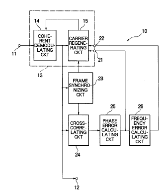
Referring to Fig. 1, description will first be
made as regards a conventional carrier regenerating
lS device 10 for a better understanding of this invention.
The carrier regenerating device 10 is for use in a mobile
station of a mobile satellite communication network which
comprises a master station for such mobile stations. It
will be assumed that a carrier signal is subjected to
modulation at the master station and with a frame period
into a modulated signal by a data signal representative
of a message and that unique words are periodically
interspersed at the frame period throughout the data
signal. The unique words are known at the mobile
stations. Such a unique word is therefore referred to
herein as a locally known unique word.
Inasmuch as the carrier signal is modulated at
the master station by the data signal or by the locally
known unique word, the modulated signal comprises a
modulated data signal and modu:Lated unique words and is
herein called a modulated overall signal. The mobile
station has a demodulator input and output terminals 11
and 12. Through a receiving unit which is usual in the
mobile station and is therefore not shown, the
demodulator input terminal 11 is supplied with the
modulated overall signal as an input modulated signal.
The carrier regenerating device is for
regenerating the carrier signal from the input modulated
signal as a regenerated carrier signal in the manner
which will become clear as the description proceeds. A
demodulator unit 13 is supplied with the input modulated
signal through the demodulator input terminal 11 and is
for demodulating the input modulated signal into an
output demodulated signal which comprises a demodulated
data signal and demodulated unique words. The output
demodulated signal is delivered to the demodulator input
terminal 12.
The demodulating unit 13 comprises a coherent
demodulating circuit 14 and a carrier regenerating
circuit 15. The coherent demodulating circuit 14 is
supplied with the input modulated signal from the
demodulator input terminal 11 and with the regenerated
carrier signal. The coherent demodulating circuit 14 is
for producing the output demodulated signal in the manner
known in the art. The output demodulated signal is
delivered not only to the demodulator output terminal 12
but also to the carrier regenerating circuit 15. The
carrier regenerating circuit 15 is for supplying a
reproduced carrier signal to the coherent demodulating
circuit 14.
Insofar as the input modulated signal is supplied
to the demodulator input terminal 11 above a
predetermined signal to noise (S/N) ratio, the reproduced
carrier signal is correctly coincident with the
regenerated carrier signal. When the input modulated
signal is delivered to the demodulator input terminal 11
with a severely attenuated level, the carrier
regenerating circuit 15 is put into a free running state.
In this event, the reproduced carrier signal may step out
of frame synchronism, namely, out of synchronism with the
frame period. As a result, the reproduced carrier signal
is undesiredly given a phase error and a frequency error
relative to the regenerated carrier signal.
In order to make the carrier regenerating circuit
15 correctly produce the regenerated carrier signal,
quadrature demodulation is used in the coherent
demodulating circuit 14. The output demodulated signal
therefore becomes a quadrature demodulated signal which
is a complex-valued signal and can be represented by real
and imaginary signal components.
The demodulating unit 13 has first and second
control terminals 21 and 22. A frame synchronizing
circuit 23 is supplied from the coherent demodulating
circuit 14 with the output demodulated signal. The frame
synchronizing circuit 23 compares a level of the output
demodulated signal with a predetermined threshold level.
When the level of the output demodulated signal is lower
than the predetermined threshold level, i.e., when the
frame synchronism is not established, the frame
synchronizing circuit 23 produces an aperture signal that
is synchronized with the locally known unique word and
that defines an aperture interval determined on the basis
of the frame period. The aperture signal is supplied
from the frame synchronizing circuit 23 to a
cross-correlating circuit 24. When the level of the
output demodulated signal is not lower than the
predetermined threshold level, i.e., when the frame
synchronism is established, the frame synchronizing
circuit 23 does not produce the aperture signal.
As a result, the cross-correlating circuit 24 is
given the output demodulated signal together with the
aperture signal. The cross-correlating circuit 24
extracts the demodulated unique words from the
demodulated data sequence and calculates a cross-
correlation between the demodulated unique words and the
locally known unique word. The cross-correlating circuit
24 thereby produces a cross-correlation signal which
typically represents the cross-correlation coefficient
and which may become large as the above-mentioned
cross-correlation becomes strong. In other words, the
cross-correlation signal has a magnitude in dependence
upon a phase error between the demodulated unique words
and the locally known unique word. At any rate, the
cross-correlation signal is de:livered from the
cross-correlating circuit 24 to a phase error calculating
circuit 25.
Supplied with the cross-correlation signal, the
phase error calculating circuit 25 calculates a phase
error which the reproduced carrier signal has relative to
the regenerated carrier signal and which may be specified
by the cross-correlation signal. The phase error
calculating circuit 25 produces a phase error signal
which represents the phase error and which is supplied to
both the first control terminal 21 and a frequency error
calculating circuit 26. As a result, the phase error is
set in the carrier regenerating circuit 15.
Responsive to the phase error signal, the
frequency error calculating circuit 26 calculates a
frequency error between the reproduced carrier signal and
the regenerated carrier signal. The frequency error
calculating circuit 26 thereby produces a frequency error
signal which represents the frequency error and which is
supplied to the second control terminal 22. As a result,
the frequency error is set in the carrier regenerating
circuit 15.
The carrier regenerating circuit 15 renders the
reproduced carrier signal into a regenerated carrier
signal in accordance with the phase error and the
frequency error.
It may be mentioned here that the carrier
regenerating circuit 15 produces the reproduced carrier
signal with a carrier signal phase angle which may or may
not be identical with a correct phase angle of the
regenerated carrier signal. Using the cross-correlation
signal, the phase error calculating circuit 25 calculates
the correct phase angle and may therefore alternatively
be called a phase calculating circuit.
Let the cross-correlation coefficient be equal to
A0 during one or a first aperture interval and be
represented by a complex value. In this event, a first
phase angle 00 is given in connection with the
cross-correlation by:
00 = arctan(Im(A0)/Re(A0)), ~.- (1)
where Re and Im represent real and imaginary signal
components of the cross-correlation signal.
It will be assumed that the cross-correlation
coefficient is equal to Ae during a next or a second
aperture interval and a second phase angle Oe is also
calculated by Equation (1).
In this event, the frequency error ~e is given
by:
~e = (Oe - 0 )/T, ... (2)
where T represents the aperture interval.
Herein, let the frequency error ~e be calculated
on the assumption that the input modulated signal has a
first carrier frequency before the input modulated signal
is not received at all and has a second carrier frequency
when the input modulated signal is again received.
Furthermore, it will be assumecl that a frequency
difference between the first carrier frequency and the
second carrier frequency is given by D~ . Under the
circumstances, a phase difference or a phase error
between the first phase angle 00 and the second phase
angle Oe is given with reference to Equation (2) by:
Oe - 00 = Ta~. ... (3)
Inasmuch as the phase difference is greater than
-~ and is not greater than ~, the righthand side of
Equation (3) may be equivalently rewritten into Ta~ + 2n~
when the absolute value of a~ is greater than ~/T, where
n represents a positive integer. Therefore, the
frequency error ~e is given by:
~e = G~ + (2n~/T). ...................... (4)
It is readily understood from Equation (4) that
the frequency error calculating circuit 26 can not
correctly calculate the frequency error.
Referring to Fig. 2, description will proceed to
a carrier regenerating device according to a preferred
embodiment of this invention. The illustrated carrier
regenerating device is different from the carrier
regenerating device 10 illustrated in Fig. 1 and is
therefore designated afresh by a reference numeral 30.
The carrier regenerating device 30 comprises similar
parts which are designated by like reference numerals and
operable with likewise named signals.
The master station transmits the modulated
overall signal to the mobile station. The mobile station
receives the modulated overall signal at the receiving
unit. The modulated overall signal is supplied as the
input modulated signal from the receiving unit to the
demodulator input terminal 11. Let the modulated overall
signal and the input modulated signal be represented by
S(t) and R(t), respectively, each of which is a
complex-valued function of time t. Using the modulated
overall signal S(t), the input modulated signal R(t) is
given:
R(t) = S(t)ej(~t+~), ... (5)
where ~ represents a frequency of the carrier signal and
~ represents a phase angle.
Let the reproduced carrier signal and the output
demodulated signal be represented by L(t) and D(t),
respectively, each of which is a complex-valued signal of
time t. Using the input modulated signal R(t) and the
reproduced carrier signal L(t), the output demodulated
signal D(t) is given by:
D(t) = R(t)L(t). ... (6)
When the reproduced carrier signal is coincident
with the regenerated signal, the reproduced carrier
signal is given by:
L(t) = e i( ). ......................... (7)
Therefore, the modulated overall signal is coincident
with the output demodulated signal at the frequency ~ and
the phase angle ~. Namely, the demodulating unit 13 can
14
correctly produce the output demodulated signal.
As described above, the frame synchronizing
circuit 23 produces the aperture signal when the frame
synchronism is not established. In this event, the frame
synchronizing circuit 23 supplies a control signal to the
carrier regenerating circuit 15. Responsive to the
control signal, the carrier regenerating circuit 15
produces the reproduced carrier signal which has a
frequency of ~.
As described above, the cross-correlating circuit
24 calculates the cross-correlation coefficient between
the output demodulated signal and the locally known
unique word.
Let the cross-correlation coefficient be
represented by A(t) which is a complex-valued function of
time t. The locally known unique word can be represented
by U(~) as a function of a parameter ~ which has a
dimension of time. The cross-correlation coefficient
A(t) is given by:
Tv
A(t) = ~ D(t+r)U*(T)dr, ~-- (8)
o
where U*(l) represents a conjugate function of the
locally known unique word, Tv represents a unique word
length.
Let the phase difference and the frequency
difference be represented by ~0 and ~, respectively.
Equation (8) can be rewritten into Equation (9).
r) ei (~r+~ ) U* (r) dT
O
= ej ~0 e d~. ~-- (9)
When a~Tv is nearly equal to zero, the cross-
correlation coefficient A(t) is given by:
A(t) = Tveia . (10)
The cross~correlation coefficient A(t) is
supplied to the phase error calculating circuit 25 and a
power calculating circuit 31. As described above in
conjunction with Fig. 1, the phase error calculating
circuit 25 calculates in accordance with the
cross-correlation coefficient the phase error which the
reproduced carrier signal has relative to the regenerated
carrier signal. It is readily understood from the
Equation (10) that the phase error calculating circuit 25
produces the phase error which is represented by a o . The
phase error ~0 is supplied from the phase error
calculating circuit 25 to the carrier regenerating
circuit 15 through the first control terminal 21.
Supplied with the cross-correlation coefficient,
the power calculating circuit 31 calculates a correlation
power of the cross-correlation coefficient. As readily
understood from the Equation (10), the power calculating
circuit 31 produces the correlation power which is
represented by ¦TVI2. The correlation power is supplied
from the power calculating circuit 31 to a signal
16
detecting circuit 32.
The signal detecting circuit 32 detects whether
or not the correlation power is greater than a prescribed
threshold value. When the correlation power is greater
than the prescribed threshold value, the signal detecting
circuit 32 supplies a detection signal to a Fourier
transforming circuit 33.
Reviewing Fig. 1, the output demodulated signal
is delivered from the coherent demodulating circuit 14 to
a frequency multiplier 34 to be frequency multiplied into
a frequency shifted signal. In the illustrated example,
the input modulated signal may be, for example, an
N-phase phase shift keying modulated signal, where N
represents a predetermined number which is not less than
two. The predetermined integer N is usually equal to 2m,
where m represents a positive number. In this event, the
frequency multiplier 34 frequency multiplies the output
demodulated signal into the frequency shifted signal by
the predetermined integer N.
Let the frequency shifted signal be represented
by M(t). The frequency shifted signal M(t) is given by:
M(t) = ~D(t)}n = eiNa~t ... (11)
The frequency shifted signal is supplied from the
frequency multiplier 34 to the Fourier transforming
circuit 33.
Responsive to the detection signal, the Fourier
transforming circuit 33 Fourier transforms the frequency
shifted signal into a Fourier transformed signal to
supply the Fourier transformed signal to a frequency
error detecting circuit 35.
As readily understood from the Equation (11), the
Fourier transformed signal has a spectrum which has a
peak level at a frequency of ND~. Therefore, the
frequency error detecting circuit 35 detects the peak
level to obtain the frequency N~. The predetermined
integer N is set in the frequency error detecting circuit
35. The frequency error detecting circuit 35 divides the
frequency Na~ by the predetermined integer N to produce
D~ as the frequency error. The frequency error D~ is
supplied from the frequency error detecting circuit 35 to
the second control terminal 22. As described above, the
phase error D o is supplied from the phase error
calculating circuit 25 to the first control terminal 21.
Responsive to the phase error and the frequency
error, the carrier regenerating circuit 15 make the
reproduced carrier signal become the regenerated carrier
signal in accordance with the phase error and the
frequency error.
In conjunction with Fig. 2, the first control
terminal 21 serves as a first correction setting
arrangement for setting the phase error at the aperture
interval in the carrier regenerating circuit 15. The
second control terminal 22 serves as a second correction
setting arrangement for setting frequency error at the
aperture interval in the carrier regenerating circuit 15.
Furthermore, the power calculating circuit 31, the signal
18
detecting circuit 32, the Fourier transforming circuit
33, the frequency multiplier 3~, and the frequency error
calculating circuit 35 collectively serves as a frequency
error calculating section for calculating the frequency
error by the use of the cross-correlation coefficient and
the output demodulated signal.
.