Note: Descriptions are shown in the official language in which they were submitted.
WO 93/0019 PCf/US92/05595
4/ ~1'~1,. 1<, ~~ ~S P
S~ ~f L/ LJ
1
~ANELROARD P~RRANGEPiENT WITH xMhROVED CONTROL
Field of The Invention
The present invention relates generally to circuit
breaker load centers and, more particularly, to improvements
in the control and monitoring of remotely controlled circuit
breakers.
Background of The Tn~rention
Remote control circuit breakers are commonly used for
temporary interruption of electrical service during peak use
hours and for programmable lighting control of industrial.._...___.__
locations. By opening and closing on demand from a remote
location, these circuit breakers provide a significant
improvement over manually operated circuit breakers in terms
l5 of convenience.
Systems using remote control circuit breakers typically
include a circuit breaker load-center having circuit breakers
wired to a remotely located computer for monitoring and/or
controlling each circuit breaker. The wiring has been
accomplished in such systems either by using a patch-board
within the load°center, as described in U.S. Patent No.
4,920,76 (Brodsky et al.), or by hard°wiring each circuit
breaker input/output to a terminal in the remotely located
computer.
Such systems, unfortunately, are not very accommodating
to system control changes. Rather, the systems are designed
CA 02089877 2000-12-15
2
to handle specific types of remote control signals, typically provided by a
5 pair of wires that may be shorted to command the circuit breaker to
close. Each time the circuit breaker control requirements change in these
systems, the wiring and many system components must be reconfigured
or replaced, thereby making these systems expensive and burdensome to
maintain.
10
Another maintenance-related problem with these types of systems
concerns the ability to control and monitor the system. Most load-center
systems fail to provide a conveniently arranged monitoring system for the
various circuit breakers and/or fail to provide a convenient method of on-
15 line circuit breaker programming.
There is therefore a need for a remotely controlled circuit breaker
load-center which is easier and more convenient to monitor and operate.
20 Summary of the Invention
It is desirable to provide an improved remote control circuit
breaker arrangement which overcomes the aforementioned deficiencies of
the prior art and which is more convenient to monitor and operate locally
25 and remotely.
It is also desirable to provide an improved circuit breaker
arrangement having tamper-proof, reliable, control for indicating
whether power to the load has been interrupted.
CA 02089877 2000-12-15
3
In accordance with one aspect of the present invention, there is
5 provided a panelboard having an enclosure and having a front side and
back wall including therein a plurality of electrical switching means, each
having a side facing the front side of the enclosure and including a multi-
sectioned user interface circuit, which is configured to communicate with
at least one of the electrical switching means. The interface circuit
10 includes a first circuit section and a second circuit section. The first
circuit section is located adjacent the back wall of the enclosure and
behind the second circuit section, and the second circuit section includes
communication means for allowing an operator at the front of the
enclosure to communicate with at least one of the electrical switching
15 means. This arrangement minimizes heat in the back of the enclosure,
provides control and monitoring functions at the front of the enclosure
and allows room for additional circuitry in the back of the enclosure.
In accordance with another aspect of the present invention, there
20 is provided a panelboard having an enclosure a front side and a back
wall, including first and second columns of electrical switching means in
parallel; and a mufti-sectional user interface circuit, configured to
communicate with at least one of the electrical switching means,
including a first circuit section and a second circuit section. The first
25 circuit section is located adjacent the back wall of the enclosure and
behind the second circuit section. The second circuit section including
means for allowing an operator at the front of the enclosure to control
and monitor said at least one of the electrical switching means. The
panelboard may further include an automatic interpreter for interpreting a
CA 02089877 2000-12-15
4
coded message which provides the operator access to control the circuit
breakers. Preferably, the coded message is received on a coded key
card.
According to another aspect of the invention, there is provided a
panelboard having an enclosure including, comprising: a plurality of
electrical switching means; a user interface circuit, configured to
communicate with at least one of the electrical switching means,
including a first circuit section and a second circuit section, and including
a circuit section located adjacent the front side of the enclosure to allow
an operator at the front of the enclosure to communicate with said at least
one of the electrical switching means and further including means for
interpreting a coded message which provides the operator access to
i c ",...,t,.m ~":a "t m".,t ...,o ~~ tw~ ,.~,..,...:....~ "...:f..w:~~
...,.~.._..
VVC) 93/00619 PCT/L'S9z/0559~
U ~)
Brief Description of the Dra~ria~as
Other objects and advantages of the invention will be
apparent from the following detailed description and the
accompanying drawings in which:
FIG. la is a perspective view of a load center
arrangement or system, according to the present invention;
FIG. 1b is another perspective view of the load center
arrangement of FIG. la;
FIG. 2 is an electrical block diagram of the system shown
in FIG. la, and including a controller, an interface module
and a termination board which are -intercoupled to provide the
primary control functions of the system;
FIG. 3 is an end view, taken along line 3-3 of FIG. la,
illustrating various interconnected components of the system
of FIG. lee
FIG. 4 is a more specific block diagram of the
controller, the interface module and the termination board of
FIG. 21
FIG. 5a is a perspective view of the display for the
2o controller shown in FIGS. 1~4T
FIG. 5b is a perspective view of an alternate display for
the controller shown in FTGS. 1-4;
FIG. 6 is a block diagram of an eacpansion module,
according to the present invention, which may be used to
interconnect a various types of accessories into the system of
FIG. la;
WO 93/00619 PCT/US92/0599~
,.'
_.
FIG. 7 illustrates a perspective view of a plurality of
systems interconnected in accordance with the present
invention;
FIG. 8 is a schematic diagram of the controller shown in
FIGS. 1-4;
FIGS. 9a-9c comprise a schematic diagram of the interface
driver board shown in FIG. 4;
FIG. 9d is a schematic diagram of the electrical portion
of a circuit breaker illustrated in FIG. tat
FIGS. 9e-9g comprise three state diagrams which depict
-the power driver, data transmit and~-data receive operation of
the gate array illustrated in FIG. 9a;
FIGS. 9h-9k comprise a series of timing diagrams which
respectively depict the receive message, open contacts, read
status and read motor operations of the gate array illustrated
in FIG. 9a;
FIG. 1O is a schematic diagram of a control bus shown in
FIG. 2;
FIGS. 11a-lld represent various implementations of the
termination board shown in FIG. ~ from a schematic
perspective; and
FIGS. 12a-12d comprise a flow chart which may be used to
program the microcomputer shown in FIG. 8; and
FIGS. 13a-13d comprise a flow chart which may be used to
program the microcomputer shown in FIG. 11a.
While the invention is susceptible to various
modifications and alternative forms, specific embodiments
thereaf have been shown by way of example in the drawings and
1~t7 93/00619 PCT/US92/0559s
will be described in detail. It should be understood,
however, that it is not intended to limit the invention to. the
particular form described. On the contrary, the invention is
to cover all modifications, equivalents, and alternatives
falling within the spirit and scope of the invention as
defined by the appended claims.
CA 02089877 2000-12-15
8
Description of The Preferred Embodiment
5
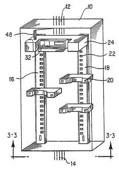
In FIG. la, the present invention is shown to provide an electrical
distribution system or arrangement which may include a panelboard or
load-center enclosure 10 which receives a plurality of input power lines
12 from a power source (not shown). Lines 14 exit the enclosure 10 to
10 distribute power to various loads (not shown). Bus boards 16 and 18,
which may be implemented on the same board, are disposed in parallel
on each side of the load-center for mounting remotely controlled circuit
breakers 20, each having a plug-in socket which is coupled to one of a
plurality of connectors 22 on the bus boards 16 and 18. The connectors
15 22 are used with the bus boards 16 and 18 to carry motor control and
contact-status signals, via an interface module 24, to and from the circuit
breakers 20. Electrical switching devices other than circuit breakers may
be used such as contractors or electrical relays.
20 A preferred circuit breaker, which may be used to implement the
remotely controlled circuit breakers 20, is described in Canadian patent
application serial no. 2089743, entitled REMOTE CONTROL CIRCUIT
BREAKER assigned to the instant assignee. Another circuit breaker
which may be used to implement the remotely controlled circuit breakers
25 20 is described in U.S. Patent No. 4,623,859, Erickson et al., also
assigned to the instant assignee.
VV~ 93/00619 PC'T 'U592/05599
~~5~ ~ ~'r~
9
As illustrated in the block diagram of FIG. 2, the
interface module 24 interprets messages from a controller 32
so as to facilitate electrical control and monitoring
functions from both local and remote locations. Both the
control and monitoring functions are accommodated within the
interface module 24 using an interface driver board 34. The
interface driver board 34 provides a communications path
between the circuit breakers 20 and the controller 32, which
resides within, and as an integral part of, the load-center
l0 enclosure lo. The controller 32 may communicate with a
remotely located control/monitoring device~35 (FIG. 7) via the
termination board 38. Any such control or monitoring signal
transmitted between the interface driver board and the circuit
breakers is carried by one of two control buses on the bus
boards 16 and 18.
The interface module 24 also includes a termination board
38, which is used to couple the control and monitoring signals
between the interface driver board 34 and the remotely located
control/monitoring device via the controller 32. Preferably,
the control and monitoring signals are transmitted and
received using either a direct-wiring (or dry contact)
interface, as depicted at port 40 of the termination board 38,
or a prescribed serial communication protocol (e. g., a wired
or wireless LAN-type interface), as depicted at part 41 of the
termination board 38. This coupling may also be accomplished
using a number of different techniques, including, for
example, those techniques discussed in U.S. Patent No.
CA 02089877 2000-12-15
10
4,709,339 (issued to Fernandez).
5
FIG. 3, which shows an end view of load-center components of
FIG. la, best illustrates the above-described electrical arrangement of
FIG. 2 from a structural perspective. FIG. 3 illustrates a manner of
interconnecting the bus boards 16 and 18, the controller 32 and the
10 interface module 24, the latter of which includes an interface module
housing 25 for enclosing the interface driver board 34, a power supply
board 44 and the termination board 38. The interface module 24 may be
coupled to the uppermost or lowermost portion of the bus boards 16 and
18 according to the preferred viewing position. The interface driver
15 board 34 is preferably coupled to the bus boards 16 and 18 via a pair of
ribbon cables 30 and associated DB25-type connectors 23, and the
interface driver board 34 is coupled to the power supply board 44 and the
termination board 38 using an interconnect board 31. The connectors 33
may be offset so that the controller 32 overhangs the top or bottom of the
20 load-center if desired. The controller 32 may be secured to the front
panel of the interface module 24 using DB-9 connectors 33.
The controller 32 includes a controller circuit board 32a which
may be secured to the front panel of the interface module 24 using DB-9
25 connectors 33. A membrane keyboard 35 is used to receive user inputs
for controlling the circuit breakers and for programming the system.
The power supply board 44 and the termination board 38 may be
implemented on a single printed circuit board or
W~ 93/00619 PC.'T/US92/05595
~1 ~ 1 r.~ ..,r r
11 ~C):.~C7
separate circuit boards. Further, a power transformer 27 is
preferably attached to the power supply board 44 to provide
power to the interconnect board 31. The transformer 27 may
include two primary windings and three secondary windings to
provide signals which may be processed using full-wave
rectifier/regulator stages, such that +5 (Vcc), -5 and -24
Volts are provided along with their associated common signals,
of which at least the latter two may be the same. In a
preferred embodiment, one secondary winding provides the +5
Volt signal, the second secondary winding provides the -24
Volts signal, and the third secondary-winding-provides an
isolated unregulated signal which is regulated to +5 Volts
(V~SQ of FIG. 11a); and the -5 Volt signal emanates from the
-24 Volt regulator.
A cover 37, including a cover door 37a rotating about a
hinge 37b, is conventionally used to .enclose the load center.
Also illustrated in FIG. 3 is a conduit mounting hole 46
on the interface module housing 25 for receiving leads, via
canduit (not shown), which connect to input terminals 54 on
the termination board 38. The leads include low voltage
wiring for switch inputs, e.g:, d1-y-contact type inputs or a
TAN. A removable termination area cover 52 protects and
allows access to the input terminals 54 of the termination
board 38.
Another important part of the present invention concerns
the location of the controller 32. As shown in FIG. 3, a
deadfront panel 70 is used to isolate the power lines from
operators and to cover the interface module 24 and most of the
WO 93/00619 ~ ~~~ PCf/US92/0559~
12
bus boards 16 and 18 and the circuit breakers 20 (FIGS. 1a and
2). The controller 32 is separated from the interface driver
board 34 and located in front of the deadfront panel 70. This
arrangement is advantageous for a number of reasons. For
instance, it provides additional room for the circuitry within
the interface module 24, which is located behind the deadfront
panel 70.
Another advantage relates to the dissipation of heat
generated by the circuitry within the interface module 24, as
well as the circuit breakers 20. Unfortunately, the deadfront
--- panel 70 has the potential to significantly increase the -
temperature resulting from the generated heat due to the lack
of ventilation that would otherwise be provided to the
interface module circuitry in the absence of the deadfront
panel 70. Thus, by locating the controller 32 and its
associated circuitry in front of the deadfront panel 70, the
termperature of the circuitry is lowered and the cost and
reliability of the circuitry is therefore improved.
Yet another advantage provided by this controller
arrangement is the additional access it provides for operator
interface. By using an informa~ionally sophisticated
monitor/control panel, such as is shown in FIG. 5a, within the
load-center enclosure l0, an operator will need complete
access to the various displays and control keys on the
monitor/control panel.
Further, this arrangement allows an operator to easily
replace or upgrade the controller without removing the
CVO 93/OOfil9 PCT/US92/0559~
13 ~~'u
deadfront panel and thereby exposing the operator to the power
lines.
In order to allow removal of the deadfront panel 70
without disconnecting the electronics between the controller
32 and the interface module 24, the controller 32 may be
coupled to the interface module 24 by a hinged pivot. In the
operating position, the controller 32 would be held in
position by a connector which attaches to the interface module
24. The opposite side of the controller would be attached by
the hinged pivot such that the controller 32 could be
--.-..- .-. perpendicularly pivoted away from-.the.panel to allow for
removal of the deadfront panel 70,
In FIG. 4, an electrical block diagram of the controller
32, the interface driver board 34 and the termination board 38
1.5 is illustrated. The controller 32 includes a microcomputer
53, preferably an MC68HC05C4 (or C8) type available from
Motorola, Inc., which communicates with a keyboard and display
panel 55 through data latch circuitry 56. The user or
operator is provided complete control over, and status of, the
circuit breakers 20 through the keyboard and display panel 55.
The controller 32 also includes electrically alterable
nonvolatile memory 57, which may be programmed by the user to
contain specific information for operating each of the
system°s circuit breakers 20. Preferably, the memory 57 does
not store the present state of the circuit breakers, since
their state may be regularly accessed from the circuit
breakers 20 themselves. However, a history of the circuit
W~ 93/Q0619 ~°CT/US92/0559s
~~~'~~'~"~'~
14
breaker activity may be recorded in the memory 57 for
maintenance purposes.
In order to prevent memory endurance problems from
limiting the life of the system, writes to the memory 57 are
limited. Variable data is .stored in the system RAM (internal
to the microcomputer 53) as long as possible before any writes
to the memory 57 are performed. Data is only written to the
memory 57 at prescribed times during the programming mode of
the controller 32. During the system run mode, data is not
l0 written to the memory 57 so as to prolong the life of the
memory. - _..... ... ... _. _ _ .
In order to prevent charge-drain off from the gates of
the individual memory transistors (internal to the memory 57),
the microcomputer 53 checks for valid data each time that the
memory is read. Charge-drain off occurs to only one
transistor at a time and is corrected by a single bit error
cads that determines the ~cralidity of the data in the memory,
Normally, the data is valid and no further action with respect
to the memory is required. However, :if an error is detected,
~0 an algorithm is run to determine if the error is a charge
drain-off error or a noise error. If it is an error due to
noise, the correct data is read again from the memory and
used. The erroneous bit will be corrected if the error is a
hard error, arid the corrected data will then be written to the
memory. This is the only instance where the memory is written
during the run mode rather than during the program mode.
Conventional circuitry 58 may be optionally provided to
provide reliable, battery-backed real-time clock functions for
dV0 93/00679 p~f/L'S92/05595
15 ~~l~v
the system. For example, this may be used to allow time-
phased events to trigger certain ones of the circuit breakers
20.
The interface driver board 34 is shown as interfacing
with the controller 32, through a data multiplexes 59, using
an optical isolator~50 to maintain voltage isolation between
the circuits and protect the circuits from power~°line
transients. The data multiplexes 59 also provides electronic
programming capabilities from a programming computer or
station 66 for accessing the controller functions. This is
preferably accomplished using serial interface circuitry 61,
e.g., for an RSa232 type protocol, between the data
multiplexes 59 and the station 66. The interface driver board
34 and the controller 32 may be coupled in this manner using a
serial protocol to reduce the number of pins required for
communication therebetween.
The interface driver board 34 further includes a gate
array 60 which couples the interface driver board 34 through
amplifiers 62 to the motors of the remotely controlled circuit
breakers 20 in order to significantly reduce the number of
required driver transistors and PC board traces. When the
interface driver circuitry is commanded to engage a breaker
(i.e., open or close the breaker contacts), the gate array 60
essentially maps the address of the circuit breaker into a
form which will turn on any two of a plurality of power output
transistors associated with the gate array 60. Timers wi~'~in
the gate array 60 drive power transistors 62 external to the
gate array 60 to control the circuit breaker motor engagement
VN~ 93/O~b~9 , ~ P(_'T/US92/OSS9~
~,
time and status read times. For example, a pair of power
transistors may drive the circuit breaker motor in either of
two directions for a controlled time period in order to turn
the circuit breaker on or off by closing or opening the
5 contacts. After the motor drive time period elapses, the
status of the selected circuit breaker is automatically read
after a specified settle time and is passed to the
communications circuitry of the gate array 60. Only one
circuit breaker can be switched at a time, and sets of
10 breakers must be turned on or off sequentially.
because of the limited physical space available for the-
power driver circuitry of the gate array 60, a minimum circuit
breaker cycle time, i.e., the time period to complete the
tasks and communications associated with a single command, is
15 observed. This cycle time allows the power supply~to
sufficiently recharge the power supply storage capacitors
(which may be located at the input of the -24 Volt regulator)
to supply full voltage to the circuit breaker motors.
The status signals provided by the selected circuit
breaker 20 are filtered by noise filters 64 before being
provided to the gate array 60, which transmits the circuit
breaker status to the controller 32 through the optical
isolator 50.
In addition to controlling and monitoring the circuit
breakers 20 from the keyboard and display panel 55, the
circuit breakers 20 may be accessed using the microcomputer 53
of the controller through the termination board 38. Far such
communication with the controller 32, the termination board 38
Wf~ 93/00619 PCf/U~92/05595
i i :1 !~~ rv
17 ~ ~ ~ ~ d~
includes a microcomputer 72 to communicate directly with the
microcomputer 53. A significant advantage of this arrangement
is that it allows a multitude of remote devices to control and
monitor the circuit breakers in the same manner as with the
keyboard and display panel 55.
The termination board 38 includes a communication or
input terminal port 54 for remote device access to the
controller 32. As previously indicated, such remote access
may be provided by hard-wiring the devices to the input
terminal port 54 with common, positive and negative leads at
wthe respective terminals. A set of--network drivers 68 may be
used to provide the requisite network interface, and
additional input circuitry 69 may be used to custom-program
interface specifications.
The input circuitry 69 may include, for example, trinary
DIP switches mounted to the termination board 38 which are
utilized to program pulsed and maintained control modes of the
plurality of inputs at terminal port 54. A single switch may
be included for each of the plurality of input terminals 54.
Each of the switches preferably have both pulsed and
maintained labels to allow the system operator set the DIP
switches according to whether the connected inputs are pulsed
or maintained.
In one application, a pulsed input may refer to any of
the plurality of input terminals at terminal port 54 which
remains active for less than sixty seconds. Using this sixty
second limitation, a maintained input then refers to an input
signal which does not make two state transitions within a time
W~ 93/00G19 PCT/US92/0559:
~ ~~c~'~,~~,
period of less than sixty seconds, a transition being an input
change between a pair of prescribed high and low voltage
levels. The microcomputer 72 then uses the DIP switch setting
to determine if an input is pulsed or maintained.
Common, positive and negative leads may be used to
control either pulsed or maintained modes. For a maintained
input, only two of the three terminals (common, positive and
negative) are used and the DIP switch is set to its maintained
position.. The common terminal is always connected for any
input. The positive terminal is connected to noxznally open
contacts, thewnegative terminal is connected-to normally
closed contacts. If a closing contact is to cause an
associated circuit breaker to switch, the two wires from the
contacts connect between the positive and common terminals.
If an opening contact is to cause a circuit breaker to switch,
the wires connect between the negative and common terminals.
If the DIP switch associated with a given input,is set to the
pulsed position, the input will be programmed to pulse mode
operation. Two or three wires are connected to the terminals
in the pulsed mode. When a positive terminal is connected, a
closing contact causes each selected circuit breaker, or group
of circuit breakers, to open or close according to the user
program. When a negative terminal is connected, the closing
contact causes each selected circuit breaker, or group of
circuit breakers, to do the opposite of the positive terminal.
The pulsed mode is useful for normally open momentary
wall switches used to override the automatic operation of the
system. A first input is programmed to turn off a selected
V~o"U 93/00b19 PCT/US92,/05S9s
2~~~er~'~
19
circuit breaker at a selected time. Next, a momentary,
normally open two position wall switch is programmed to
control the same circuit breaker using a second input. The
system turns the selected circuit breaker on automatically
when the contact of the first input is closed. The circuit
breaker turns off when the contacts of the first input are
open. The momentary switch of the second input may override
the state of the contacts. If the switch is placed in the on
position, the circuit breaker turns on regardless of the state
of the contacts. Likewise, if the switch is pushed off, the
associated circuit breaker would turn off.regardless of the
state of the contacts.
The cont~~~ctor may optionally include a feature in the
system while setting the input terminals wherein the system
may autostep to used inputs while skipping unused.inputs
during programming. To enable this feature, the contractor
sets the corresponding trinary DIP switch to the center
position. When in program mode, the system looks for these
shorts and does not display them on t;he front panel of the
controller such that the user cann~t program them. If this
conditi~n is not present, the system shows the inputs on its
display during normal programming. The programmer may choose
not to program these inputs thereby achieving the same result.
If the condition is not present, the pulsed or maintained DIP
switch settings are ignored.
The controller 32 initiates all communications to the
gate array 60 by sending a two byte message which minimizes
communications protocol errors. The first byte of the two
W~ 93/0a619 ~,r~~~, PCT/US92/0559~
~~ ~~ ~..i
transmitted bytes is equivalent for communications either to
or from the interface driver board 34 or controller 32. A
byte number is placed in the least significant bit position of
all transmitted bytes to reduce the chance of unsynchronized
5 messages. Accordingly, bit zero of the first byte always has
a value of zero because it indicates the byte number. Bits
one through four indicate the circuit breaker address and are
the least significant bits of a particular circuit breaker
address. Bits five through seven are check bits which are
20 generated to check bits one through four. The format far the
--------- second byte of a message differs depending on whether it is -
sent from the interface driver board 34 or the contrdller 32.
Messages sent from the controller 32 are command bytes. In
the second command byte, bit zero is always one because it
15 signifies byte two of the message. Bits ane and two are the
most significant two bits of the circuit breaker address.
Bits five through seven are generated to check bits one
through four. Bits three and four are encoded with four
possible commands to the interface driver board 34. The
20 controller commands are to read the motor, read the contact
status, open a selected breaker or close a selected breaker.
When the mast significant bit of the command code is a zero,
the interface driver board 34 only sends back a status. If
the most significant of the two bits is a one, a switch
command is sent to the interface driver board 34.
Messages sent from the interface driver board 34 are
status bytes. The second byte of a status message may differ
from the second byte of a command message in bit positions
WO 93/00b19 PCT/U~92/OS59S
~~3~~~ ~~~
21
three and four. In a status byte, bit four is a status and
bit three is always zero. These bits indicate the presence of
a motor in the circuit breaker, the status of the contact,
i.e., whether a selected breaker has been opened or closed.
If the interface driver board 34 detects an attar in
either byte one or byte two, no circuit breaker switching or
status reading occurs. An all 1's error message is returned
and the interface module is reset to wait for the first byte
of the next command. The controller 32 then retransmits the
previous message. Accordingly, if the controller 32 sends a
-read status message, the int.erfacerdriver board 34 reads the -
circuit breaker status and returns the results to the
controller 32. Tf the controller message is a switch command,
the interface driver board 34 carries out the command by
switching the breaker. Tt then reads and returns. the contact
status of the selected breaker. The :interface module response
to a read status message is the desired status of the contacts
of the selected circuit breaker. The interface module
response to a switch command is the actual status of the
2~ contact after the switch has occurred. The controller 32 uses
the returned information to ascertain whether the selected
circuit breaker has switched. If the returned status shows
that the contacts are in the wrong state, the controller 32
may be programmed to attempt to correct the problem.
A seven bit cyclic hamming code detects errors in the
most significant seven bits of a message byte. The byte
number bit is excluded because there is no available hamming
code which will detect seven bits with three check bits. The
WO 93/00519 P~.'f/U592/05595
22
'~'1~ ~~
exclusion is insignificant since parity detects any odd bit
error in any bit position. If a two bit error occurs in any
message byte which includes bit zero, the hamming code will
detect it because the other seven bits of the byte are checked
by the code. If a controller command is retransmitted
multiple times and an unexpected status is received from the
gate array 60, the controller may be programmed to display the
error and may then discontinue transmitting the command
thereby assuming that the circuit breaker has failed.
1o As can be seen in FIG. 5a, the keyboard and display panel
which is sh~wn in FIG. 4 is preferably i~ipleinentsd as part of
a flip-open housing which encloses the controller circuitry of
FIG. 4, except for portions of the keyboard and display panel
55. The controller 32 comprises a system display which
provides an interface to allow a user to program the system
responses according to the programming provided at the input
circuitry 69 of the termination board 38.
The system may operate in any of four modes: run, halt,
manual or progl~am. The run mode represents the normal
operation of the system, including provision of the primary
functions of controlling and displaying the status of the
circuit breakers. when tine system is first powered on or
comes up after a power down, it may enter the run mode. In
this mode, the controller 32 may drive the system display,
scan the control buttons, and look for changes at the
plurality of inputs.
The system regularly scans all of the circuit breaker
status lines and displays the results on a plurality of hEDs
WO 93/00619 '~ ~ ~ ~~ ~~ ~~ ~ PCTIL'S92/0559~
23
90. The LEDs 90, which indicate the open or closed status
position of the circuit breakers 20 are conveniently arranged
to correspond to the arrangement of the circuit breakers 20 as
viewed from the front of the load center (as shown in FIG.
la). When the system commands a circuit breaker to switch,
the actual status of the circuit breaker will be displayed on
a status indicator display 92. The status of all of the
remotely controlled circuit breakers appears in the same
configuration as the breakers are arranged in the load-center.
The breaker statuses may be polled only periodically, rather
than constantly, to avoid communications--protocol traffic and
reduce panel temperatures. Preferably, however, the breaker
statuses are polled as fast as possible so as to provide
immediate responses.
When the front cover 94 of the fa-ont panel 96 is closed,
the status indicator 92, the breaker :status button 98 and the
breaker select button 100 are accessible to the user. While
the enter button 102 is accessible to the user only when the
front panel 96 is open, these buttons 99 and 100 allow a user
to switch a selected circuit breaker and display the breaker
status on the status indicator 92 while in the run mode.
Instructions (not shown) may be affixed to the exterior of the
front coven- 94 to instruct the user as to operations for
switching circuit breakers during the run mode.
The display will display the number of the last circuit
breaker which the user programmed or manually switched. The
status display 92 indicates, whether that breaker is open,
closed or unaffected by the switch. If the breaker statuses
WO 93/00619 PCT/LJS92/U5595
n
(', 4:;~.'L,~ a
6?~v"' 24
are polled only periodically, the breaker status indicator 92
is blank in order to limit the amount of power continuously
dissipated in the circuit breaker status read circuitry. Tf
the status beds 90 were on continuously, power would be
dissipated in the opto-isolator drive circuitry raising the
temperature inside the breaker to that which may exceed the
opto-isolator specifications.
In order to manually open or close a selected circuit
breaker, the user selects the desired circuit breaker by
pressing the breaker select button 100 until the number of the
-- --desired circuit breaker appears in-the breaker-display 104. -
each time that the breaker select button 100 is pressed, the
system automatically scans for the next installed circuit
breaker. The position of the circuit breaker that is found is
displayed in the breaker display 104. The user continues to
press the circuit breaker select button 100 until the number
of the selected circuit breaker appears in the breaker display
104. The circuit breaker that is manua:Lly switched will
remain in the desired state until another manual or automatic
signal causes it to switch.
Alternatively, the status indicator display 92 and the
breakers status. button 98 may be replaced by status indicator
lights and a breaker status button located on the front of the
load-center dead front 70 next to each circuit breaker 20.
When the system is in operation, the indicator light of each
breaker is lit when the breaker is on, and is unlit when the
breaker is off. When the programmer selects an input by using
Vb'~ 93/0069 PC."T/U~92105595
~~kt,~~~~~
~ .~ ~;7 s
the input select button 100, the desired circuit breaker is
selected by pressing the button next to that breaker.
When the front cover 94 is opened, additional buttons and
display become accessible. The system mode is selected using
5 the run mode button 108, the halt mode button 110, the manual
mode button 112 or the program/review mode button 114. When
the system first enters the run mode from either the halt or
manual modes, it scans the terminals at input terminal port
54. Since pulsed inputs are lost in both the half and manual
10 modes only the maintained inputs are available for scanning.
As the inputs are scanned, the equations for all-of the
available circuit breakers are solved, and the breakers are
switched accordingly. After this initial scan, the system
reverts to normal run mode operation and scans both pulsed and
15 maintained inputs. The system regularly scans the-inputs and
display buttons while driving the various display devices.
There are no other controller actions until an input
transition occurs, or a button is pressed.
If an input transition occurs, the microcomputer on the
20 termination board will debounce and interpret the input. The
microcomputer on the controller receives the interpretted
input from the termination board and then switches the circuit
breakers accordingly. Similarly, if a button on the front of
the controller is pressed, the microcomputer on the controller
25 will debounce, process, and act on the user input according to
the function of the button. As the circuit breakers are
switched, their actual status is displayed on the status
WO 93/00519 PCT/L~S92/0559~
26
indicator 92. .Additionally, the last input which goes through
a transition is displayed on the input display 116.
The system enters the halt mode when the halt mode button
110 is pressed by the user. The halt mode ignores the
plurality of input terminals 54 and leaves the system in its
present state. Once the halt mode is entered, the system
remains there until the user presses another mode button.
System status information is not stored while in the halt mode
such that if a pulse occurs it will be missed. To exit the
halt mode, the user presses any of the other three mode
buttons. If-the system is halted and either-the-manual or
program/review button is pressed, the selected mode is entered
with no further action from the controller 32. If however,
the run mode is entered after the halt mode, the system will
scan all programmed inputs and set the system circuit breakers
according to the values present on the maintained inputs.
Pulsed inputs that occurred prior to entering the run mode are
not acted upon.
The manual mode is entered by pressing the manual made
20 button 112. In the manual mode, the system seguentially
switches all circuit breaker motors to their on state and then
displays the current status on the status indicator 92. This
action places the circuit breakers in a mode which emulates
standard manual circuit breakers. While in this made, the
circuit breakers can only be controlled by the handles of the
individual breakers because all inputs are ignored as in the
halt mode. The manual mode differs from the halt mode in that
it changes the state of the circuit breakers to their on
~'1'O 93/OOb~9 PCf'/L'S92/0559s
~~~~i~~s"~
27
position. When the system is in the manual mode and either
the halt or program/review buttons are pressed, the system
immediately enters the new made withaut further action by the
controller. If the run mode button is pressed, the system
scans the maintained inputs and sets the affected breakers
accordingly.
The program/review mode is one means by which the system
may be programmed. This mode is used to enter, modify or
review circuit breaker control programs. The user presses the
program/review button 114 to enter the program/review mode.
When this mode is entered, the systemwremains-in the run mode
from the standpoint of the system°s reaction to input
transitions. The system continues to process input
transitions even if the user is programming the circuit
breakers. Unlike the other operating modes, the
program/review mode has an auto exit ~:eature. If no button is
pressed for a selected time period while the system is in the
program/review mode, the system reve~ta to its previous mode.
Upon entering the program/review mode, the input channel
to be programmed is displayed in the input display 116 and the
circuit breaker to be programmed is displayed in the breaker
display 104. The input display 116 and breaker display 104
are incremented or decremented by using the input select
button 106 and breaker select button 100, respectively. As
described above, the system automatically scans for the next
installed selection as either of these buttons is pressed. If
no circuit breakers are installed in the system, the system
display is blank in order to prevent a never ending loop.
WO 93/00679 '' ~,_~''~ f(_'T/dJS92/OS59~
~c~: ~-~a ~)
'U v
28
When the + button of the respective buttons 106 or 100 is
pressed, the inputs or breakers are scanned in ascending order
and the next available input or breaker is displayed.
Conversely, if the - button of the buttons 106 or 100 is
pressed, the next available input or breaker is displayed
after scanning the inputs or breakers in descending order. In
program/review anode, the status indicator 92 will display how
the circuit breaker on the breaker display 104 will respond to
the input on the input display 116 rather than displaying the
l0 actual circuit breaker status. The input signal type is
--displayed on the signal display 118 as maintained or pulsed:
To aid the programmer in configuring the system, a
technique is employed to ease understanding of the logical
connections. The programmer completes a sentence for each
input, wherein the sentence is '°When input (number) detects a
(pulse or maintained) signal, the bre<gker (number) (opens,
closes or is unaffected)." This sentsance is printed on the
input and breaker display area of the display panel. The
programmer simply enters the input number, signal type,
breaker number and desired circuit breaker status and presses
the enter button to program the system. No permanent program
saving function occurs until the enter button is pressed. If
enter is not pressed, the front panel button can be pressed
without permanently changing the program. This method is used
to review the program content.
An input which overrides all other inputs for a given
circuit breaker may be programmed by the user as a pulse
input. This input is defined as an override off and is
WAD 93/00619
PCT/U~9210559~
~U'{~U~~~
29
represented on the display. panel 55 by an open circuit breaker
status light on the status indicator 92 while in program made.
An override off input opens a given circuit breaker regardless
of the status of the other inputs. If a selected input is not
programmed as an owerride off, it remains unprogrammed or is
programmed as a normal input.
The circuit breakers 20 of FIG. ~.a are numbered in two
columnss circuit breakers in the left column start at one and
are odd numbered, and circuit breakers in the right column
start at two and are even numbered. The LFDs 90 are
-- preferably arranged and numbered 'in-the display of FIG. 5a to
correspond physically to the arrangement of the circuit
breakers 20 of FIG. la.
An example may be helpful to explain the convenient
manner in which the display of FIG. 5a may be programmed and
monitored to control the circuit breakers 20 of FIG. 1a. In
this example, a user is to program a three pole circuit
breaker occupying circuit breaker positions numbered 7, 9 and
11 and a single pole breaker in circuit breaker position Z6 to
be in the same states at the same time. Assume that inputs A,
B and C are connected to terminals 1, 2 and 3 (of the eight
input terminals of the termination board 38) respectively, and
the override off input is connected to terminal 12. Inputs A,
B and C will be normally open maintained contacts. An
override off will be a pulsed input. The first three
terminals have one contact wire connected to its positive
terminal, and one wire connected to its common terminal. The
DIP switches associated with inputs l, 2 and 3 are set to the
WO 93/OO~bl9 PC1'/U892/05595
C' ~v~°~~ ~
positions corresponding to the maintain mode. The override
off input wires are connected to the positive and common
terminals and the DIP switch is set to its pulsed position.
The motor pole of the three pole breaker is in the center and
5 is in circuit breaker position number 9, and the single pole
breaker motor will be in circuit breaker position number. l6.
Proceeding from left to right on the front display panel,
input 1 is selected by pressing the input select + button
until a 01 appears in the input display. Next, the user
10 selects the desired circuit breaker by pressing the breaker
select + button until a 09 appears in thewbreaker display 104.
Each time the + button is pressed, the system automatically
searches for the next breaker motor. This method eliminates
the possibility of a user programming an unused circuit
15 breaker position since empty circuit breaker positions do not
appear in the display. when the 09 ap;psars in the breaker
display 104, the status appears on the status display and
MAINTATN appears on the signal display signifying that the
input is maintained. An appearance of a maintained signal is
20 to cause a circuit breaker to close; therefore, the breaker
status button 98 will be pressed until the LED next to
°'CLOSES" is lit and the CLOSE LED associated with breaker in
position 9 in the open/close LED array also lights. While in
this program.~ning mode, all LEDs associated with the circuit
25 breakers to be controlled by the displayed input will light as
either an open or close.
At this point, the programmer can press any of the
buttons without danger of changing any of the programming. If
W~ 93/Ofl619 ~ PC.'TlL~S92/05995
~1 ~~ r
tJ ~ .j'
31
the operator presses the halt made button, the system will
enter the halt mode without changing anything. If the
operator fails to press a button far a given controlled time,
the system will revert to its previous state automatically.
However, if the enter button is pressed, the information on
the current display will be permanently stored in memory. The
status display will momentarily flash to signify that the
breaker is now permanently programmed.
After breaker 9 is programmed using input 1, breaker 16
is programmed by pressing the breaker select button until a 16
appears in the-breaker display. When the-16 appears in the
breaker display, the current breaker program appears in the
status display and MAINTAIN appears signifying that the input
is maintained. The breaker select butaon is pressed until the
LED next to '°CLOSES°° lights. After the enter button
is
pressed, the input display will displ<iy a 01. The breaker
display will contain a 16, and the status display close lights
will be on in the 9 and 16 positions. Ndte that while in
program/review.mode the status indicator display displays the
affect that one input has on all of the breakers. After
programming all breakers associated with a given input,,the
next input is selected by pressing the input + button once so
that a 02 appears in the input display. The breaker and
breaker status are selected as described above. The same
procedure is followed for input 3.
Now that the three inputs A, B, and C are programmed, the
override off input is programmed to complete the programming
operation. The input + button is pressed until a 12 appears
Vd~ 93/00619 ' iy' ~ F'C'T/U592/0959s
c,4~u'
32
in 'the input display and the pulse light appears on the signal
display to signify that the input is a pulse. The breaker
number is then selected as described above. Programming
proceeds as described above except that status open is
selected instead of status closed. When the enter button is
pressed, the status indicator display shows a closed light
under circuit breakers at positions 9 and 16 to signify that
the input and breakers are programmed. Note that the override
off input will override any of the other inputs regardless of
ZO their states to open the circuit breakers at positions 9 and
._ _ .._ _ .._ _._. 16.~ _ _ _
An alternative display embodiment of the present
invention is illustrated in FIG. 5b. In this embodiment, a
three-step programming configuration i:~ used in place of the
sentence-programming configuration discussed above in
connection with the embodiment of FIG. 5a. In terms of
fuaaction, this display embodiment is the same as the display
shown FIG. 5a: thus, the reference num:arals depicting the
various components in FIG. 5a are used to depict the
corresponding components in FIG. 5b.
The primary difference between the respective embodiments
of FIGS. 5a and 5b is that the enter or "LACK-IN" button of
FIG. 5a is replaced by the °'enter" buttom in FIG. 5b. Rather,
the display of FIG. 5b locks in the programmed inputs when the
system returns to the RUN mode via button 108.
As a controller circuit option, unauthorized access to
the programming function of the controller 32 may be prevented
using a key card mechanism 103 (FIG. 5a) to lock out the
CA 02089877 2001-05-22
33
programming function. The key card 103 comprises a small durable card having a
pattern of
holes wherein the card is designed to be placed into a card slot 105 in the
front of the
controller 32. An LED/photo detector combination located within the controller
32 detects
the presence of the key and determines the particular function from the key
card pattern. The
key card allows access to particular modes of operation thereby providing
security for the
system. An exemplary key card mechanism is described in U.S. Patent No.
4,489,359.
FIG. 6 illustrates an expander panel 130 which may be optionally coupled to
one or
more load centers, such as the load center 10 shown in FIG. la, to provide a
number of
communication-related features to l:he load center shown in FIG. la. The
expander panel 130
is enclosed in a housing 132 and may include a microcomputer 134 for
controlling
communication with the load centers. A power supply 136, fed by a conventional
AC line,
may be used to provide power to the circuits contained within the housing 132,
and a network
driver circuit 140 may be used to interface the microcomputer 134 with a
communication
network or protocol required for communication with the load centers.
By employing one or more terminal ports 142 within the housing 132, external
devices may be electrically coupled to the microcomputer 134 for additional
kinds of remote
control and monitoring of the circuit breakers, their associated current paths
and other
PnninmPnt accnriatPrl with the ~.nntrnllPr TrlPallv the mir.rnrnmrn~tPr 1'~4
rnmm~miratPc
WO 93/00619 ~ PCT/L'S92/0559~
.~1~~
(.,~ 34
through the network driver circuit 140 of FIG. 6 to the
controller 32, via the network drivers 68 of the termination
board 38 (FIG. 4). LAN or other types of conventional
communication protocols may be used to implement this kind of
interface, as previously discussed.
The expander panel 130 may also include one or more
option cards (or circuits) 144 for providing customized
functions. In a preferred embodiment, one of the option cards
144 is a telephone interface circuit, which is designed using
conventional techniques to provide access to the controller 32
(FIG. 4) through standard telephone lines: ether option cards
144 may include, for example, an input expander card for
allowing additional devices to be coupled into the system, an
isolated RS232 computer interface, data logging memory with
battery back-up, data logging printer interfaces, telephone
network access card, telephone modem e:ards, wireless (FNi)
communication links and fiber optic repeater cards. The
functions described in the expander panel may be built and
installed as separate functional elements.
The expander panel, which has plug-in modularity, may be
used to provide a number of network-communication type
features. Although multiple load center (such as 10 of FIG.
la) may be networked without the expander panel, FIG. 7
exemplifies an application in which a plurality o.f load
centers may be connected in a LeAN by networking the load-
centers 10 with one ~of the expander panels 130 of FIG. 6.
This kind of arrangement can provide significant maintenance-
related savings when used in an industrial-type application.
aW~ 93/00619 ~ ~ . ~CI'/US9Z/05595
Turning now to the schematic diagram of FIG. 8, the
controller 32 (from FIG. 4) is shown with the keyboard and
display 55 (FIG. 4), the real-time clock circuitry 58, the
data multiplexer 59 and the-RS-232 interface circuitry in
5 detail. The keyboard and display 55 includes a 10-key
membrane keypad 160 which is regularly scanned using a four-
by-three switch matrix. To detenuine which, if any, of the
membrane keys have been depressed, the microcomputer 53
latches logic "0"s from each of four bits from the
10 microcomputer's C port into a latch 162, and it polls three
bits from the same port to determine if any--of--the-three bits
are shorted to one of the latched faux bits by the depression
of the associated membrane switch. Pull-up resistors 164 bias
the three polled bits so that a logic ''1" is read at each
15 polled bit if the associated four switches are not depressed.
The latch 162 and the microcomputer°s C port are used in
combination with the microcomputer°s A port to control all of
displays on the controller 32, including~four 7-segment I~ED
package displays 165°168. As discussed in connection with the
20 breaker display 104 and input display x.16 of FIG. 5a, the
displays 165-168 are used to identify for the user or operator
the particular input (at the termination block 38) and circuit
breakers being addressed by the keypad. A network of eight
Darlington transistors 170 is coupled to the output of the
25 latch 162 to provide the proper drive level fdr display matrix
for which the outputs (A-H) of the transistors 70 drive the
row side of the matrix. The column side of the display matrix
is driven by 8 bits which are provided directly from the A
dV0 93/00619 PCT/iJS92/0559a
~°'o
.-.'7 a
36
port sf the microcomputer 53 and 8 bits which are provided
indirectly from the A port, via latch 172, to enable each LED
of the displays. Because the display does not require being
display-refreshed more than 40 times per second, the
microcomputer 53 is able to use its C port to monitor the
keypad 160 and control the displays 165-168 without conflict.
The microcomputer 53 employs the latch 172 at the output
of its A port to control stand-alone NO CHANGE, CLOSE and OPEN
LEDs and four columns of a 7-by-5 dot matrix display 176. The
A port of the microcomputer 53 directly controls stand-alone
RUN, HALT, MANUAL, REVIEW, PULSE AND MAINTAIN LEDs and four
columns each of 7-by-5 dot matrix displays 177 and 178. The
displays 176-178 are used to indicate the contact positions of
the 42 circuit breakers represented by the status indicator
display 92 0~ FIG. 5a. The three displays 176-178 are
configured so that only four columns o;f each are used. thereby
providing 28 LEDs on each part so that the 84 required
displays (two per circuit breaker) are accommodated.
A variety of staple components may be used to implement
the circuit illustrated in FIG, 8. For example, the latch 162
may be implemented using a 3-8 74HC137 encoder-type IC, while
the latch 172 may be implemented using a 74HC373-type IC. The
displays 165-168 may be implemented using a HDSP7503-type
part, and the displays 176-178 may be implemented using a
HDSP4701-type part. The RUN LED is preferably implemented
using a green HLMP-1790 part, and all other stand-alone LEDs
are preferably implemented using a red HLMP-1700 part. Each
LED type is available from Hewlett Packard Co.
~O 93/00679 PC?/US92/05596
3~,~3J~~ ~
Conventionally, displays are controlled by sequentially
turning on one digit or display group at a time, but
repetitiously and sufficiently rapid so that all devices
appear to be on simultaneously. The requisite driving current
(or power) for such conventional displays is proportional to
the number of segments that are turned on in each display
device. Accordingly, as each display is sequentially
switched, the amount of current drawn from the power supply
can vary significantly. For example, no current flows if all
segments are off, while the maximum current flows if all
~- -- segments are on. The power supply in such conventional
displays must, therefore, be able to supply the peak value of
the current, even if the average value is much less.
The display design of the present invention provides a
significant improvement over this deficiency of the prior art.
The display on the controller 32 is preferably designed and
controlled to provide a significant reduction of peak power
usage. This design multiplexes the display elements by
grouping segments together from different displays, rather
2o than treating each display as a group. If the variation from
minimum to maximum is kept as small as possible, the peak
value of current is reduced, allowing a smaller and lower cost
power supply to be used.
In accordance with the display design described above,
attached hereto is an Appendix A whicz illustrates a table for
controlling the LEDs of the display. The table includes 128
status entries defined by 16 rows'and 8 columns. The entries
are grouped to multiplex the display elements by grouping LED
W~ 93/00619 Pt.'f/1_J592/0559~
.T~~,a ~.~ .
38
segments together from different displays to lessen power
usage as described above. Preferably, two pairs of rows at a
time are read by the microcomputer and written out the
parallel buses to update the status of each corresponding LED.
For example, the first row includes: two bits to designate
the proper status of circuit breaker 16 - one bit is for its
OPEN LED and the second bit is for its CLOSED LED; two bits to
designate the proper status of circuit breaker 15 - one bit is
for its OPEN LED and the second bit is for its CLOSED LED;
etc. The OPEN and CLOSED LEDs are either both off or one of
them is on: therefore, only three of t2is fc~ur~stat~s provided
by each pair of circuit breaker status entries are used.
The second row of the table includes: a bit to designate
the proper status of segment A of the 7-segment display 4
(D4Sa) (display ~, e.g., corresponds to display 168 of FTG.
8); a bit to designate the proper status of segment A of
display 3 (D3Sa); . ; two bits to designate the proper
status of circuit breaker 30 ~ one bit is for its OPEN LED and
the second bit is for its CLOSED LED: etc. The bottom two
rows of the table include the proper status of the labeled
LEDs on the display, such as Maintain, Pulse, Review, etc.
Since all segments in these groups will never by on, arranging
the devices in this manner results in a lower peak current for
the worst-case condition.
Also within the Appendix A and below the table is a
program written in MC68HC05 assembly language code which may
be used as a basis for controlling the display using the table
W~ 93/OOby9 PCT/L'S92/05595
~~ v ~ci ~ ~'
39
of Appendix A in the above described manner, and with the
microcomputer updating the LRDs at about 40 Hertz.
Certain ones of the C port peripheral bits may be used to
program and read the EPROM 57, which may be implemented using
an X24C16 type IC, and to reset the microcomputer 72 of the
termination board when necessary. Also, a reset IC 174, such
as an MC34164 IC, along with conventional RC timing circuitry
may be used to reset and interrupt the microcomputer 53 upon
power-up and when power decays during power down or due to
other low voltage occurrences.
The real-time clock circuitry 58-is-optional--to the
remaining circuitry of the controller 32 and may be used to
provide time-based circuit breaker control functions. For
example, the microcomputer 53 and the real-time clock
circuitry 58 may be programmed by the programmer station 66
(FIG. 4) so that the real-time clock is polled by, or
interrupts, the microcomputer at one or more prescribed
periods to inform the microcomputer 53~that it is time to open
or close a current path associated with a certain circuit
breaker. In response to this type of prompt, the
microcomputer 53 commands the designated circuit breaker to
open or close its associated current path, provided that a
command of a higher priority for the same circuit breaker was
not received by the microcomputer 53 before the prompt
occurred.
Commands of various priorities which may be received by
the microcomputer 53 for the same circuit breaker, in addition
to the aforementioned programmed prompt from the real-time
WO 93/00619 ''~~~ la ~ PC1'/L'S92/05595
J
clock, include a variety of commands sent through the
termination board 38 (FTG. 4), commands received from the
programmer station 66 (FTG. 4) and commands received from the
keyboard and display 55 (FIG. 4). Tt is preferred that the
order of priority for conflicting commands is that: commands
received from the keyboard and display 55 are treated as the
most important due to servicing requirements; commands
received from the programmer station 66 are treated as the
second most important since servicing may also be performed
from the programmer station 66; commands sent through the
--termination board 38 are treated as-the next most important; -
and commands prompted by the real-time clock are treated as
the least important since they are likely to be representative
of a previously desired mode and, therefore, requiring an
override via one of the higher priority conunand paths.
The real-time clock circuitry 58 .is preferably
implemented using a 3.0 Volt Lithium battery 202 to backup an
MC68HC68T1-type real-time clock IC (integrated circuit) 200.
A pair of LM393A-type amplifiers 204 may be used to monitor
the battery 202 by comparing the voltage level of the battery
202 to a stable reference voltage level (Vref), e.g., about
2.3 Volts, at lead 206. For additional information concerning
the implementation of the real-time clock circuitry 58,
reference may be made to the data sheets and application notes
for the MC68HC68T1 IC, available from Motorola, Inc.
The data multiplexes 59 is used by the microcomputer 53
to route data to and from both the programmer station 66 and
the gate array 60 of the interface driver board 34. Data is
W~ 93/00619 PCT/US92/05599
41
passed to and from the programmer station 66 using a
conventional RS-232 interface circuit 61, e.g., using a
bT1180-type IC, while the data passed to and from the gate
array 60 is pracessed using an asynchronous, serial-data
protacol. As depicted in FIG. 8, data is passed to and from
the microcomputer 53 via its RDO and TDO ports through the
data multiplexer 59, which is preferably implemented using a
74HC4052-type IC. A peripheral bit on the microcomputer 53,
depicted as CHEN, is used to select {or "enable") one of two
channels through the data multiplexer 59. The first channel
- ~- couples the TDO and RDO ports of the xnicrocompi~ter 53 with
comparable ports of the gate array 60 of the termination board
38, and the second channel cauples the TDO and RDO ports with
the transmit and receive ports of the RS-232 interface circuit
61. Another peripheral bit on the microcomputer 53, depicted
as EN, is used to enable the RS-232 interface circuit 61 so
that its CTS and RTS signals are inactive when the RS-232
interface circuit 61 is not being used.
The microcomputer 53 communicates with the microcomputer
72, with the former acting as the master and the latter acting
as the slave and with each microcomputer 53 and 72 employing a
conventional crystal oscillator circuit 161a or 161b which
drives the respective microcomputer at 3.6864 Mega-Hertz.
Three of the bits from the D port of the microcomputer 53 may
be. respectively employed as the data transmit, data receive
and synchronous cloak paths for communication with the
microcomputer 72 of the termination board. For example, using
the MC68HC05-type microcomputers to implement the
W~ 93/00b19 ,' ~,.~'''~ PCT/US92/05595
,a
42
microcomputers 53 and 72, the MISO (master-in-slave-out), MOSI
(master-out-slave-in), SCK (synchronous clock) and SS (slave
select) microcomputer pin-outs (FIGS. 8 and 11a) provide an
adequate interface. The protocol preferably includes error
detection and error correction schemes to prevent erroneous
messages from causing the interface driver board 34 to execute
an incorrect command. For example, if an erroneous message is
received by the interface driver board 34, the protocol
detects the error and corrects it in a subsequent message from
l0 the controller.
FIGS. 9a-9c illustrate the interfaee-driver board 34 of
FIG.4 schematically. The optical isolator 50, the gate array
60 and the status filters 64 are depicted as in FIG. 4.
However, the representative amplifiers 62 from FIG. 4 are
shown as circuit breaker row drivers 2:L2 and circuit breaker
column drivers 214. The other element: shown will be
introduced and discussed in turn.
The interface driver board also includes a conventional
oscillation circuit 217 which is used to provide the
appropriate clock (e. g., a 455 kHz clock) for the gate array.
For further information regarding the gate array 60, reference
may be made to the data sheets published and made available by
ACTEL, Inc. of Sunnyvale, California.
The optical isolator 50 is preferably implemented using
two NEC2501-1 type parts with resistors 218-221 (R a 1k Ohm in
FIGS. 9a-9d) providing the appropriate bias at the inputs and
outputs of the optical isolator 50.
WO 93/00619 PCI'/US92~0569~
43
The circuit breaker row and column drivers 212 and 214
are configured seven down and six across, respectively, for
controlling the motors of the forty-two circuit breakers 20 of
FIG, la. Each row driver 212 is used to select (or enable)
the circuits of six circuit breakers, while each column driver
214 is used to actuate the circuit breaker motor which. is
selected by the intersecting row driver 212.
Each status filter 64, which is used to report whether
the contacts of the circuit breaker are open or closed, are
operative when two conditions are present: the corresponding
column driver 214 must select'the column of circuit breakers
in which the status filter 64 is associatedt and the gate
array 60 must actuate a triac circuit (e. g., a Siemens IL420)
to provide, simultaneously, a momentary common path (LED COMM
on the bus boards 16 and 18) for the input ports of the
optical isolators 230 (FIG. 9d) of all forty-two of the
circuit breakers 20. The gate array 60 then reads all six
statures and determines which of these statures are to be sent
to the controller 32. The circuit breaker contacts are
preferably monitored using a lead 231 (FIG. 9d) connected to
the load terminal of the circuit breaker 20.
A varistor 228, such as a GE-V30DLA2, is coupled across
the output ports of the triac circuit 226 to provide circuit
protection against voltage and current transients.
In FIG. 9b, the column driver 214 is shown as being
controlled by the gate array 60 using CDa, CDb and MSTAT leads
so as to drive the motor on the selected circuit breaker 20.
The diodes 232 through which the motor drive signal passes are
WO 93/00619 ,~~''~ PCT/US92/OS59~
V~
44
located on the bus board 16 or 18 to allow a current path
through only one circuit breaker 20. The CDa and CDb signal s
from the gate array 60 are controlled in a polarized manner
between -5 Volts and common.so that if either signal is
absent, the designated circuit breaker 20 cannot be commanded
to open or close its contacts.
The MSTAT signal is used to indicate whether or not a
motor is present. This type of status check operates in
substantially the same manner as the statuses from the
associated circuit breaker load, as described above. The
- -MSTAT signal is operative whew the corresponding column driver
214 selects the column of circuit breakers associated with the
circuit breaker under test. The gate array 60 then reads all
six MSTAT signals and determines which of these signals are to
be sent to the controller 32.
In FIG. 9c, the row driver 212 is shown as being
controlled by the gate array 60 using RDa and RDb leads so as
to select the appropriate row of circuit breakers 20. The
diodes 238 and 239 are used to mitigate the effect of
transient signals received from the bus boards 16 and 18.
FIG. 9d, which illustrates the electrical control portion
of the preferred remote control circuit breaker 20, degicts
four leads carried by each plug-in connector 22 of the bus
boards 16 and 18. They include: the select lead 246, status
lead 248, motor drive lead 250 and an isolator enable lead
252; the signals of each lead performing the previously
described functions.
i~VVO 93/00619 fCf/i,~S9210559s
A parallel resistor/diode arrangement 254/256 serves two
functions. The diode 254 may be used to provide current flow
in a unilateral direction, while the resistor 256 is used to
control the power provided from lead 258 to the motor of the
5 circuit breaker 20. The value of the resistor 256 is selected
according to the necessary current specified to operate the
motor. In the event that the lead 258 is used to control a
plurality of poles, e.g., for controlling two or three circuit
breaker poles, the resistance required will vary. For single
10 pole operation by the FIC130S°10300 Mabuchi motor exemplified
-in the above referenced copending application, the value of
the resistor 2S6 is preferably 12 Ohms.
FIG. 9e is a state diagram which depicts the power driver
operation of the gate array illustrated in FIG. 9a. The
15 diagram includes six states, depicted A-F. Beginning at state
A, the gate array waits for a command from the controller.
The command may be one of four commands: a close contacts
command which instructs a particular circuit breaker to close
its contacts, depicted by the sequence of states A-B-D-E-A: an
20 open contacts command which instructs a particular circuit
breaker to open its contacts, depicted by the sequence of
states A-G-D-E-AJ a read contacts command to determine if a
particular circuit breaker's contacts are closed or open,
depicted by the sequence of states A-E-A; and a read motor
25 command to determine if the motor is present, depicted by the
sequence of states A-F-A. The state delay associated with
state D is to allow the contacts sufficient time to settle
before reading the status of the contacts at state E. The
iV0 93/U~619 1 ~ FC'("/U~92/0~59~
a.
C.~'~~J
.i" 46
state delays associated with states B and C are to allow the
contacts sufficient time to react before commencing the
settling-time delay of state D. The state delays associated
with states E and F are to provide the gate array with the
appropriate timing response before reporting to the controller
with the requested status.
FIG. 9f depicts the message transmit operation of the
gate array illustrated in FIG. 9a in state diagram form. The
diagram includes four states, depicted G-J. Beginning at
state G, the gate array waits for flow from states E and F for
- transmitting a contact status or motor status response. Once
received, flow proceeds to block H where the first of the two
bytes is transmitted. Since each byte consists of a start
bit, 8 data bits, a stop bit and a parity bit, an 11 bit delay
is illustrated. From state H, flow p:roceeds to state I where
the gate array waits for prescribed interbyte delay before
moving to state J. At state J, the second of the two bytes is
transanitted, arid, after the 11 bi.t de:Lay, the transmission is
complete.
FIG. 9g depicts the message recea.ve operation of the gate
array illustrated in FIG. 9a in state diagram form. The
diagram includes states K, L and M. Beginning at state K, the
gate array is reset and flow proceeds to state, L to wait for
reception of the first byte of the two-byte message from the
controller. If the first byte is received with an error, flow
returns to state K for corrective action (e.g., a reset and a
communication to the controller that an error occurred). Once
the first byte is received, flow proceeds to state M where the
W~ 93/00519 PCT/US92105595
y! p1 Pe
~i 'if ~ ~ 0
47
gate array waits for the second of the two bytes. Once the
second byte is received, the gate array determines whether or
not the second byte was received with an error. If the second
byte is received with an error, flow returns to state K once
again for corrective action. Otherwise, the reception of the
second byte completes the reception mode for a two-byte
message and flow returns to state L.
The gate array 60 is preferably implemented using an
ACTEL A1020APL84I-type gate array which is fused according to
to the information attached hereto in Appendix B, which includes
parts I-IV. - Part I is the fuse file, ~ciliicti constitutes the
main input to the ACTEL fusing program for the subject part.
To save space, the file is presented with seven parallel
columns of fusing data, which is read t:op to bottom./ left to
right. To actually use the file, the :even columns of data on
each page must be converted to a single: column on the far left
of the page. Part II is a definition file which is also
required to program the subject ACTEL s~evice. Part III is a
gate array pin list which is also presented to the ACTEL
fusing program so that the program can determine which pins
correspond to which device circuits. The parenthetical
comments to the right of the PIN numbers may be used to
correlate the listed PIN numbers to the schematics of FIGS.
9a, 9b and 9c.
Part IV consists of four sheets of commands sent from the
controller and proper responses from dhe gate array. The
first sheet includes 42 commands which may be used to instruct
each of the 42 circuit breakers to report as to whether or not
W~ 93/0619 ~~.''~ PCT/L~S92/05595
~. : ;' ; ~, ''
48
a motor (or circuit breaker) is present in the load center.
The second sheet includes 42 commands which may be used to
instruct each of the 42 ,:ircuit breakers to report as to
whether the associated circuit breaker contacts are open or
closed. The third sheet includes 42 commands which may be
used to instruct each of the 42 circuit breakers to open the
associated contacts; the response by the gate array is one
which indicates whether the contacts are open or closed after
the controller command is executed. The fourth sheet includes
42 commands which may be used to instruct each of the 42
w-- circuit breakers to close the-~ssociated contacts: the
response is similar to that for the open command in that the
gate array indicates whether the contacts are open or closed
after the controller command is executed.
FIGS. 9h-~9k comprise a series of taming diagrams which
respectively depict the receive massage, open contacts, read
status and read motor timing operations of the gate array.
There are fourteen signals shown in the figures: RCV is the
receive signal (and gate array pin) which is used by the gate
array to receive a two byte message from the controller;
ENABLE SAMPLE is an internal signal to the gate array which
tracks the timing for receive data sent between the controller
and the gate array; XMIT is the send signal (and gate array
pin) which is used by the gate array to transmit a two byte
message to the controller; DRVTRIAC corresponds to the
isolator enable lead 252 and is an active low signal (and gate
array pin) which is used to drive the triac circuit 225 when
the gate array is preparing for a status read; DRVCOND
ifO 93/00619 PCT/L~S92/05595
~~ r~
~'~~~os:f
49
corresponds to the signal 219 of FIG. 9A and is driven low
when the status is not actually being read - when this signal
is low, the status filters drive the inputs to the gate array;
PSEL#-bRV and NSEL#-DRV are active low signals which are
respectively used to drive the select or row drivers 212
during status/motor read.and open command execution (where #
designates one of the six rows); PMOT#°DRV and NMOfi#-DRV are
active low signals which are respectively used to drive the
PNP and NPN motor or column drivers 214 during open command
execution and close command execution (where # designates one
~- of the seven columns); PS[] represents the combination of all
PNP select or row power transistor drivers 212; NS[]
represents the combination of all NPN select or row power
transistor drivers 212; PM[] represents the combination of all
PNP motor or column power transistor drivers 214; and NM[]
represents the combination of all NPN motor or column power
transistor drivers 214. The PS[], NS[], PM[] AND NM[] are
denoted in hexidecimal form in each of the diagrams.
FIG. 9h illustrates byte 0 and byte 1 being received by
the gate array from left to right, with the least significant
bit being on the left and the most significant bit being on
the right. The enable sample signal being high indicates when
the gate array latches in a bit from the receive signal. The
bit definitions for each byte are the same. Each includes an
active low start bit, a byte number bit (0 for byte 0 and 1
for byte 1), four data bits for the message, three check bits
for detecting communication errors, a parity bit and an active
WO 93/00619 "~°'~~~ PCf/US92/05595
high stop bit. The notation tb~t represents 1/1200 second bit.
width for a 1200 baud rate transmission.
FIG. 9i illustrates the gate array timing when an open
contacts command is being received and executed. At point i-a
5 of the diagram, the two byte message or command is received by
the gate array. At point i-b, the triac is enabled, and at
point i-c the particular column and row drivers for the
designated circuit breaker are enabled to open the circuit
breaker contacts. The hexadecimal representation of NS[] and
10 PM[] (5F and 3B) reflect one bit of the row drivers and one
bit of the coltamn drivers being low so as to select the
correct circuit breaker from the circuit breaker array. At
point i-d, the gate array prepares to read the status of the
circuit breaker contacts, and at point i-a the gate array
15 begins reporting the status of the circuit breaker contacts to
the controller.
FIG. 9j illustrates the gate array timing when a read
status command is being received and executed. At point j-a
of the diagram, the two byte message or command is received by
20 the gate array. At point j-b, the triac is enabled, and at
point j-c the particular column driver for the designated
circuit breaker is enabled to allow the CSTAT signal to read
the selected falter. At point j-d, the gate array begins
reading the status of the circuit breaker contacts, and at
25 point j-a the gate array begins reporting the status of the
circuit breaker contacts to the controller.
FIG. 9k illustrates the gate array timing when a motor
read command is being received and executed. The only
WO 93/00619 PCT/L'S92/0559~
j 'l
i.: z.
51
substantive difference between the signal transitions of the
diagrams FIGS. 9j and 9k is MSTAT is used in place of CSTAT.
FIG. 1O illustrates one of the identical bus boards 16
and 18 of FIG. 4 from a schematic perspective. Shown are
twenty-one connectors 22 for each of the twenty-one remote
control circuit breakers 20. Each connector 22 carries each
of the four signals (the select lead 246, status lead 248,
motor drive lead 250 and the isolator common lead 252) between
the interface driver board 34 and the circuit breaker 20. The
l0 diodes 232 are also illustrated and discussed in connection
with the circuit in FIG. 9b. The connectors~26O or 261-may be
used to connect the bus board 16 or 18 with the interface
driver board 34 at either the top or the bottom, respectively,
of the load cewter 10. The diodes 232 are used to provide
currant blocking sa that only one motor can be selected at a
time, and the diode 262 is used to provide current blocking so
that all the current must flow through the opto triac circuit
226, rather than through the other various available paths.
FIGS. lla-11d represent various aspects of the
termination board 38 in considerably more detail than FIG. 4.
FIG. 11a, by itself, illustrates each of the components of the
termination board 38 in schematic form, except for certain
matrix circuitry 272 which is shown schematically in FIG. 11d.
FIGS. llb and llc illustrate terminal blocks 270 (implementing
the input terminals 54 of FIG. 4), which may be used for
connecting dry-contact switches or relays to the termination
board 38.
W~ 93/00639 PC.'T/US92/05595
r
52
The microcomputer 72 of FIG. 11a, which may be
implemented using the same type of IC as that used for the
microcomputer 53 of FIG. 8, controls the termination board
using ports A, B and C, along with certain designated bits
from the D port for serial communication. The A port is used
to scan or read the terminal blocks 270 (illustrated as part
of the matrix circuitry 272) in a highly efficient manner, as
will be discussed. The B port and the first three bits of the
C port are used to read a set of nine trinary DIP switches
274. The C port may also be used for controlling a multi-
ww -w-w color hED 27G, via resistor 278, to provide diagnostic-related
information regarding the operation of the termination board.
The matrix circuitry 272 is optically isolated from the
remainder of the termination board 38 using a pair of quad NEC
PS2501-4 ICs, opto-couplers 280 and 282, so as to isolate Vcc
(and its common) from Viso (and its common) to protect the
termination board circuitry from induced electrical noise
received from the remote control devices connected to the
teraninal blocks 272 and to block the radiation of noise into
the wiring. The A port bits A:o-3 are individually received
at the anode side of the four inputs of the opto-coupler 280
and coupled past a pair of transient protecting diodes 284 to
provide four optically isolated control bits C1 thraugh C4,
which are used to drive four calumns of the matrix circuitry
272. The eathode side of each of the four inputs of the opto-
coupler 280 is preferably connected to Vcc (+5 Volts) through
820 Ohm pull-up resistor.
dV0 93/Og6~9 PCf"/L'S92/05595
7Mlrv
2~~4~~> > ~
53
Four rows of the matrix circuitry 272 are read by the A
port bits A:4-7 via four optically isolated control bits R1
through R4. Each of the control bits R1 through R4 is
individually received at the collector side of an associated
one of the four outputs of the opto-coupler 282 and coupled
from a low pass filter circuit 288, which removes high
frequency noise. From the low pass filter circuit 288, each
control bit R1 through R4 is received at the anode side of a
respective one of the four inputs of the opto-coupler 282,
which couples R1 through R4 to the A port bits A:0-3. Each of
~~ the collector outputs of the opto-coupler 282 are pulled to
Vcc via 1k Ohm resistors 290.
Tn the matrix circuitry 272, C1 through C4, which are
normally at a logic high, are alternately set low (0 Volts)
while the microcomputer 72 scans each of R1 through R4 for
each Cl through C4. If any switch input, e.g., defined by P2-
P3 in the upper left corner of the ma~t:rix circuitry 272, is
shorted, the microcomputer 72 is then able to detect that
short by scanning R1 through R4.
FIO. lid illustrates the matrix circuitry 272
schematically, with each of the switch pairs (e.g., P2-P3, P8-
P9, P17-P18, etc.) shown separated out for illustrative
purposes. The diodes 300 are selectively placed to prevent
the microcomputer 72 from falsely determining that one of the
switch inputs is in the shorted state. Without the diodes
300, such a condition could occur if, for example, the
adjacent three switch inputs (forming a square in the matrix)
iW~ 93/00619 PCTlUS9Z/0559s
~r
t~v..~j~~~y ~ 54
a
we~e'~each shorted simultaneously. The diodes 302 are used to
provide transient protection.
FIG. llb illustrates a preferred manner of arranging the
switch inputs, each of. which is labeled with a circle around
the respective number 1-8, such that a three-wire signal,
having positive, common and negative (as previously
discussed), may be received by each of the switch inputs to
control one, or a set, of the circuit breakers 20. The
terminals of each switch input, e.g., P2, P3 and P4, are
designated in FIG. 11b to indicate the corresponding switch
input in FIGS . -11a and l 1d . _ . __ _ ._ ._. .. _.
FIG. 11c is used to illustrate the proper manner of
connecting the signal wires to the switch inputs. Embodiment
III illustrates a preferred way of wiring a three-wire pulsed
(momentary) or maintained signal at a ;single one of the eight
switch inputs, while embodiment IV illustrates a preferred way
of wiring a two-wire maintained signal at a single one of the
eight switch inputs. The embodiments depicted I and II
respectively illustrate an acceptable manner of connecting two
two-wire signals and an unacceptable manner of connecting a
three-wire signal (or two two-wire signals) to the switch
inputs. In order to avoid false switching or undetected
switching, no three-wire signals should be connected across
vertical terminal blocks 270 thus, embodiment I is proper and
embodiment II is improper. The dotted lines in each terminal
block depict a shared common between the wire terminals, and
each terminal block includes only three wires terminals for a
total of 24 possible wirs terminals.
WO 93/00619 PCT/U592/05595
55 ~~~ ~<j ~~
Eight of the nine trinary DIP switches 274 are used to
program the microcomputer 72 for the kind of remote control
signal (e.g., pulsed or maintained) which is to be received at
each of eight input terminals (FIGS. 11b and 11c), as
previously discussed. As an alternative, the function of the
first eight trinary DIP switches 274 may be implemented by
programming the microcomputer 72 through the controller 32
(e.g., via the programmer station 66) or through one of the
inpt.at terminals (assuming that the microcomputer 72 has a
known default mode for receiving this information). The
--- remaining one of the trinary switches 274 is used~to program
the microcomputer 72 for the network configuration. For
example, each of the three positions of the remaining trinary
switch can be used to indicate point-to-point, multidrop
(e. g., RS485-type) and a disable network communication mode,
respectively.
Each of the trinary DIP switches 274 is read by the
microcomputer 72 by scanning the center terminal 304 of the
switches 274, while, alternately, driving a logic low on each
outside terminal 306 or 307. By pulling up to Vcc each of the
center terminals 304 using pull-up resistors 308, the
microcomputer 72 is able to determine the position of each
trinary switch 274.
As previously discussed in connection with the
microcomputer 53 of FIG. 8, the SCLK, MOSI, MISO and SS ports
of the microcomputer 72 are directly connected with the
corresponding ports of the microcomputer 53 of FIG. 8 to
provide synchronous serial communication therebetween.
W~ 93/08619
PCT/TJS92fU559s
56
Although not shown, a pair of diodes may be situated on each
of the lines emanating from the SChK, MOSI, MISO and SS ports
to provide protection from both high and low level power
transients.
The network drivers 68 of FIG. 4 are preferably
implemented using an LTC-485 type IC 310, which is optically
isolated from the microcomputer-related circuitry using NEC
1?52501 type opto-couplers. The purpose of the optical
isolation is to eliminate noise and ground-loop related
problems. This conventional arrangement may include
--~----~ ~- transient-resistant diodes to provide -reliable and efficient
RS485 type network capabilities for the system.
FIG. 12a illustrates a preferred flow chart which may be
used to implement the operating program for the microcomputer
Z5 of the controller 32 of FTG. 4. The flow chart begins at
blocks 400 and 402 where the microcomputer is depicted
transitioning from the reset to system initialization stage.
At block 404, a test is performed to ds~termine if any signal
transitions have been detected at the input terminals of the
tex~ination board. As previously discussed, any such signal
transitions are interpreted by the termination board 38 and
passed to the microcomputer of the controller 32 via the
synchronous link. Once the microcomputer of the controller 32
receives notification of such a signal transition, flow
proceeds from block 404 to block 406 where the microcomputer
determines which circuit breakers are associated with the
signal transition and which tasks must be scheduled in
accordance with the signal transition. From block 406, or if
WO 93100619
PCT/US92/0559~
r; y
57
no signal transition was detected at block 404, flow proceeds.
to block 408.
At block 408, the microcomputer performs a test to
determine if any manual inputs have been received and
debounced via the timer interrupt routine of FIG. 12c. In
response to the reception of such an input, flow proceeds from
block 408 to block 47.0 where the requisite tasks associated
with that input are processed. From block 410, or if no
manual input was received at block 408, flow proceeds to
ZO blocks 412 and 414 where. the microcomputer performs any tasks
which have been scheduled for executions for example, such a
task would include any automatic action to be taken as a
result of a prompt from the real time clock. From blocks 412
and 414, flow returns to block 404 for additional monitoring
of the signal inputs at the termination board and the manual
inputs at the front panel of the controller 32.
FIG. 12b illustrates a preferred manner of receiving the
two-byte message from the gate array. The flow chart begins
at block 483 where the microcomputer ;receives a byte via an
interrupt: At block 484, the microcomputer determines if the
second byte (byte 1) has been sent to the gate array for a
proper response. If not, flow proceeds to block 485 where the
microcomputer sets a flag indicating an error (e. g., both
bytes must be transmitted before a valid response can be
received) and that corrective action needs to be taken.
Otherwise, flow proceeds to block 486 where the microcomputer
constructs and interprets the received message from the gate
array. At block 487, the microcomputer checks for errors. If
WO 93/00619 ~. ?_a,y, y
PCT/US92/0559s
58
an erroneous response was received, flow proceeds to block 488
where an appropriate error flag is set for subsequent action.
Otherwise, flow proceeds to block 489 where the microcomputer
determines whether byte 0 or byte 1 has been received. If
byte 0 was received, a flag is set (block 490) to indicate
that another byte is forthcoming. If byte 1 was received, a
flag is set (block 491) to indicate that a valid message was
received and, if needed, further action taken. From blocks
485, 488, 490 and 491, a return from interrupt command is
executed.
FIG. 12c illustrates a flow chart whick~ may be used to
implement a timer interrupt routine for the microcomputer 32.
This routine services, upon the receipt of the timer
interrupt, various inputs to the controller including the
switches on its front panel. The routine starts at block 450
where the microcomputer of the control:Ler is depicted being
interrupted from its normal flow. From block 450, flow
proceeds to block 452 where the microcontroller updates the
display as previously described. At block 454, the
microcomputer refreshes its internal COP (computer operating
properly) register to prevent a reset from occurring. Block
456 depicts the microcomputer presetting the counter which is
used to generate the next timer interrupt.
From block 456, flow proceeds to block 458 where the
microcomputer performs a test to determine if there are any
switch inputs at the front panel of the controller that have
to be processed. If there are any switch inputs that have to
be processed, flow proceeds from block 458 to block 460 where
W() 9~/006y9 PCl"/~,'S92/0559~
~;~i~'~n~'::l
9
59
the microcomputer debounces the next unprocessed switch input.
Any such manual input is preferably debounced using
conventional software debouncing steps. If there are no
switch inputs that have to be processed, or from block 460,
flow proceeds to block 462.
At block 462, the microcomputer performs a test to detect
switch transitions caused by manual inputs at the front panel.
If such transitions have occurred, flow proceeds to block 464
where flags (bits) are set to record which switches have been
selected. Otherwise, flow proceeds to block 466.
docks 466 through 476 represent a tim~oixt girocedux~s to
ensure that the gate array is responding to the commands sent
from the controller. If the gate array does not respond
within a certain time limit (block 468) by returning the
rec;uisite acknowledgement or status report, the associated
timer is cleared and an error flag is set (block 472) for
appropriate action during the main flora chart (block 412 of
FIG. 12a). If the gate array responds within the time limit,
flow proceeds from block 468 to block 474 where the timer
counter is incremented for the next pass through block 468.
Before exiting the routine at block 478, any restoration of
system registers occurs at block 476.
FIG. 12d illustrates a more detailed perspective of a
preferred manner of sending the two-byte message from the
controller to the gate array. The flow chart begins at block
479 where the microcomputer determines if the first byte (byte
0) has been sent yet. If not, flow proceeds to blocks 480
where the microcomputer resets a flag indicating that byte 1
....,
VSO 93/00619 c. ~ "C, '' ~~
PCT/LS92/05595
s
has been transmitted, then transmits byte 0, and then sets a
flag indicating that byte 0 has been transmitted. If the
microcomputer determines that the first byte has been sent,
the opposite occurs at blocks 481; the microcomputer resets a
5 flag indicating that byte 0 has been transmitted, then
transmits byte 1, and then sets a flag indicating that byte 1
has been transmitted. This subroutine, which may be called
from block 412 of FIG. 12a, is exited at block 482.
FIGS. 13a~13d respectively illustrate a main routine, a
10 timer interrupt routine, a serial communications interrupt
" routing, and a serial peripheral interrupt routine as a
preferred manner of programming the microcomputer of the
termination board 38 (FIG. 11d). FIG. 13a begins at block 493
where the microcomputer is depicted transitioning from the
15 reset to initialization stage. At black 494, the
microcomputer scans the trinary DIP switches to determine the
configuration set by the operator.
At blocks 496 through 500, the microcomputer scans,
debnunces and decodes all inputs to dei~ermine which tasks must
20 be executed. Activity flags, as depicted at black 502, may be
set to record the types of tasks to be performed. Blocks 504
and 506 depict the microcomputer checking for and displaying
errors that may have transpired via the scanned inputs. Other
tasks may also be processed at this point in response to
25 messages or flags being sent from any of the other routines.
From block 506, flow proceeds to block 508 where the
microcomputer waits for the timer interrupt routine to prompt
VSO 93/00619 PCT/U992/05595
~~4~~31~~
61
another reading of the DIP switches and other inputs to the
microcomputer.
The timer interrupt routine, illustrated in FIG. 13b and
beginning at block 516, comprises two basic steps, depicted at
blocks 518 and 520. At black 518, the microcomputer sets a
background flag to indicate that the time has come to once
again scan the DIP switches and other inputs to the
microcomputer. Thus, when the microcomputer returns from
block 508, it proceeds to block 494.
i0 From block 518, flow proceeds to block 520 where the
~irii-crocomputer refreshes an internal conventional watchdog
timer circuit (e. g., an internal COP register), which protects
the microcomputer from entering into nonprogrammed modes.
Other watchdog routines may also be implemented at this point
to ensure proper operation external to the microcomputer. The
interrupt routine is exited via block 522.
The serial communications interrupt routine, illustrated
in FIG. 13c, illustrates a preferred manner far the
termination board to communicate with external devices via the
network drivers. Tyke routine begins at blacks 526 and 528
where the microcomputer enters the routine and checks the
network address to determine if the communication over the
network contains the destination address of the subject
termination board. At blocks 530, 532 and 534, the
microcomputer stores, validates and flags the communication.
The message flag set at block 534 may be executed, for
example, in the main routine of FIG. 13a or the interrupt
routine of FIG. 13d, depending on the particular type of
Wf) 93/0d619 . ''~ ~! PC1'/U592/0559~
~~.; ~~a
sz
message. The routine is exited at block 536 via a return from
interrupt command.
FTG. 13d illustrates a preferred manner for the
termination board to communicate with the controller board
via the previously discussed master/slave interface. The
routine begins at blocks 538 and 540 where the microcomputer
enters the routine and retrieves the command being sent from
the controller. At block 542, the microcomputer calls the
appropriate subroutine for executing the command sent from the
controller. For example, the microcomputer may be instructed
to send the current status of each of the eight input~switches
to the controller. Tn this instance, the microcomputer would
call a subroutine which reads the status of each switch and
transmits that data to the controller. The routine is exited
at block 544 via a return from interrupt command.
While the invention has been particularly shown and
described with reference to a few particular embodiments, it
will be recognized by those skilled in the art that
modifications and changes may be made to the present invention
described above without departing from the spirit and scope
thereof. For instance, the termination board 38 may be used
as one of several types of circuit boards used to interface
with various types of outside devices and/or to provide
varying levels of control to the circuit breakers.