Note: Descriptions are shown in the official language in which they were submitted.
'W~ 92/05951 PCf/US91/06~66
_1_
2~~a:~.t~
~RASaorr wE~R RESasT~r~ o~~~~~ su~smRA~~ ~ROD~acx
FIELD OF THE INVENTION
This invention relates generally to coated
substrate products. More particularly, the invention
relates to a substantially optically transparent coated
substrate product comprised of a parent substrate, one or
more interlayers and a diamond-like carbon layer, and to
a method for producing same.
BACKGROUND OF THE INVENTION
The properties of glass make it an ideal
substrate material for use in many applications. In
particular, the combination of optical transparency, with
reasonable strength at a nominal cost, allows the
widespread use of glass products. Glass, however, does
suffer from several limitations. Glass is not a
particularly hard material, and conseguently it abrades
in many applications. Additionally, glass is~ chemically
reactive with many alkaline substances and with
hydrofluoric acid. New applications and superior
performance in existing applications could be thus
realized for glass products if glass were more abrasion
resistant and less chemically reactive. Examples of
glass produots which could benefit from improved abrasion
resistance include eyeglass and sunglass lenses,
architectural glass, analytical instrument windows,
automotive windshields and laser bar code scanners for.
use in retail. stores and supermarkets.
Diamond-like carbon films (DLC) are well known in
the,:art and have been recognized as potential coatings to
enhance the abrasian resistance of various substrate
materials, including glass. The.DLC. coatings possess
excellent optical properties andexhibit excellent
"", resistance to abrasion and chemical attack by various
acids, including hydrofluoric acid. However, at has been
found that the DLC coatings will impart improved abrasion
I~VO 92/05951
PCT/US9l/06~66
2
~
r~
stance to a substrate only if the adherence of the
coating to the parent substrate is excellent.
The most obvious and common approach to coating
the glass substrate is to apply the DLC coating directly
onto a clean glass surface. However, this approach often
results in a DLC coating which displays poor adhesion and
therefore, poor abrasion resistance. DLC coatings are
typically under significant compressive stress. This
stress greatly affects the ability of the coating to
remain adherent to the glass substrate. Additionally,
glass often contains many alkali oxides and other
additives which can inhibit the bonding of the Sio2 in
the glass to the carbon atoms in the DLC coating. It is
currently believed that the reaction between the Sio2 in
glass and the DLC is essential for the coating to exhibit
excellent adhesion. Therefore, less obvious methods are
required to produce a glass substrate with a highly
adherent DLC coating which provides excellent abrasion
resistance.
In addition to glass substrates, many other
optically transparent substrata: materials, such as
sapphire, glassy-ceramics, salts (NaCi, KBr, KC1,
etc.), metal fluorides and metal oxides could benefit
from a DLC coating, but contain elements which inhibit
- 25 the bonding of the DLC layer.
Many methods for"depositing DLC have been
demonstrated, including radio frequency plasma
deposition, :'ton beam sputter deposition from a carbon
target, ion beam sputtered carbon with ion beam~assist,
direct ion.beam.deposition, dual ion beam deposition, I
.laser ablation deposition from a carbon target, and ion
.beam assisted:evaporation of carbon.~~Mariy of these prior
- .art techniques have been used to'~deposit DLC~on glass
substrates, however, the emphasis of the prior~art has i
not been on: the adhesion of the DLC to the glass
.,, substrate or on the abrasion resistance of the coated
. ,-,
W~ 92/05951 P(.'f/iJ591/06~5b
3- ~~~'~ ~ 0
substrate product. Illustrative are the following
references: U.S. Patent Nos. 4746538, 4400410, 4383728,
4504519, 4603082, 4060660, 4877677, 4569738 and 4661409;
Japanese Patent Nos. 63221841, 63221840, 63195266,
1147068, 1147067, 64--2001, 59-26906 and 51128686;
European Patent Nos. DD-203903, SU1006402, European Patent
Application #~EPO 243541 (WO 87/02713); Deutchman, et al.,
Proc. SPIE-Int. Soc. Opt. Eng. 1146, 124-34, 1989;
Collins, et al., Proc. SPIE-Int. Soc. Opt. Eng. 1146, 37-
4?, 1989; Liou, et al., Proc. PIE-Int. Soc. Opt. Eng.
,1146, 12-20, 1989: Bubenzer, et al., Proc. DARPA Workshop
Diamond-Like Carbon Coat., Meeting date 1982, Tssue AD-
A136 766, 33-47, edited by B. Bendow in NBS Spec. Publ.
669, 249-54, 1984; NBS Spec. Publ. 638, 482-82, 1984;
Bubenzer, et al., NBS Spec. Publ. 638, 477--81, 1984;
Appl. Phys. Lett. 55, 631-3, 1989; J. Vac. Sci. Technol A
7, 2307-10, 1989; and D. Nir, Thin Solid Films, 144, 201-
9, 1986. These references do not however describe the
use of transparent interlayers to improve the adhesion of
the amorphous carbon coating to the substrate.
It is therefore an object of this invention to
provide a coated substrate product with superior abrasion
wear resistance and reduced chemical reactivity.
It is a further object of this invention to
provide a diamond-like carbon coating to the surface of an
optically transparent substrate which is highly adherent
and exhibits superior abrasion wear resistance.
It is a further object of this invention to
provide a coated substrate with improved ease of
_- cleaning. '
It is a further object of this'invention to
provide a low cost and efficient process~~for producing a
coated substrate product with superior abrasion wear
resistance.
SUMMARY OF THE INVENTION
The disclosed abrasion wear resistant coated
WO 92105951
~~ PCT/US91/06866
.
~~~ -4 -
substrate product substantially reduces or eliminates the
disadvantages and shortcomings associated with the prior
art techniques. The invention discloses a substantially
optically transparent composite structure which comprises
a parent substrate, one or more intermediate layers and
a
diamond-like carbon layer. The invention also discloses
a method for fabricating the coated substrate product.
According to the method, the substrate surface is
initially chemically de-greased. In the second step, the
substrate surface is bombarded with energetic gas ions
to
assist in the removal of residual hydrocarbons, as well
.. as alkali metals and other additives. After the
substrate surface has been sputter-etched, one ar more
interlayers are chemically vapor deposited on the
. 15 substrate, followed by the deposition of a diamond-like
carbon layer. Once the requisite number of interlayers
and diamond-like carbon layers have been deposited, the
coated substrate is cooled and removed from the reactor.
BRIEF DESCRIPTION OF THE DRAWINGS
Further features and advantages will become
apparent from the following and more particular
description of the preferred embodiment of the invention,
as illustrated in the accompanying drawings, in which
like reference characters generally refer to the same
parts or elements throughout the views, and in whiche
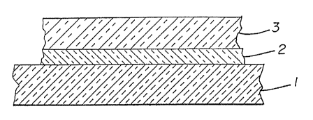
Figure 1 is a cross-sectianal.view of the coated
substrate, product in accordance with the present
invention;
Figure 2 is a cross-sectional view of the coated
substrate product in accordance with a further embodiment
of the prevent inventions and
. , =, Figure 3 is a cross=sectional view of the coated
substrate product in accordance with a still further
embodiment of the present invention.
DETAILED DESCRIPTION OF THE TNVENTION
In accordance with the present invention, the
'WO 92/05951 PCT/US91/06866
-5- ~~~'~:~~~J
disclosed abrasion wear resistant coated substrate
product substantially reduces or eliminates the
disadvantages and shortcomings associated with the prior
art techniqtaes. As illustrated in Figures 1-3, the
disclosed invention is a substantially optically
transparent composite structure which comprises a parent
substrate, one or more intermediate layers (interlayers)
and a diamond-like carbon layer. By the term of
"substantially optically transparent", it is intended to
mean transparent to light in the visible region of the
electromagnetic spectrum, which.is generally between 350
nanomete:rs and approximately 750 nanometers wavelength.
A highly important technical advantage of the invention
is that the resultant multilayer composite structure
produces a highly abrasion wear resistant surface on
various substrate materials, particularly glass.
In the preferred embodiment form of the
invention, as illustrated in Figure 1, a first interlayer
2 (or adhesion-mediating layer) is chemically vapor
deposited onto a parent substrate 1 which comprises aw
substantially optically transparent amorphous material, a
single crystal, polycrystalline materials, glass, salt
materials, ceramic materials and/or mixtures thereof. By
the term of "Chemically vapor deposited", it is intended
to mean materials deposited by vacuum deposition
processes, including. thermal evaporation, electron beam
evaporation, magnetron sputtering, ion beam sputtering
from solid precursor materials; thermally-activated
deposition from reactive gaseous precursor materials;
glow discharge, plasma, or ion beam deposition from
_, gaseous precursor materials. Preferably, the first
interlayer 2 is deposited onto the parent substrate 1 by
ion beam or magnetron sputtering.
Atmospheric pressure deposition methods including
arc-spray or plasma-spray deposition from gaseous or w
solid precursor materials, or thermally-activated
'CVO 92/0595'1 ~ ~~~, ~a PCT/US91/06866
~ i~'' -6-
w
deposition from reactive gaseous precursor materials may
additionally be employed to deposit the first interlayer
2.
The first interlayer 2 generally comprises a
. 5 substantially optically transparent material devoid of
alkali metal atoms and fluorine, and capable of forming
a
strong chemical bond to the substrate 1 and the diamond-
like carbon layer 3. By the term of "strong chemical
bond", it is intended to mean that the interlayer is
composed of a significant amount of an element or
elements which are capable of undergoing a chemical
reaction with carbon to form carbide-bonding. The
. absence of alkali metals and fluorine is essential to
achieve a highly adherent interface between the first
interlayer 2 and the diamondlike carbon layer 3. Thus,
the first interlayer 2 must also have the property of
providing a barrier to diffusion of alkali metals and
additives from the parent substrate 1 to the diamond-like
carbon layer 3.
In the preferred embodiment form of the
invention, the first interlaye:r comprises silicon oxide,
silicon dioxide, yttrium oxide, germanium oxide, hafnium
oxide, tantalum oxide, titanium oxide, zirconium oxide
and mixtures thereof. By the term "oxide", it is
intended to mean a stoichiometrically oxidized material,
or.a partially oxidized. material which contains excess
metal atoms, or is deficient in oxygen. The first
interlayer may further comprise silicon nitride,. titanium
nitride, tantalum nitride, hafnium nitride, zirconium
nitride, boron nitride; silicon carbide, germanium
carbide and mixtures 'thereof. By the term "nitride", it
is intended to mean a material composed of a
stoichiometric amount of nitrogen or a material which
either contains excess nitrogen atoms, or is deficient
in
nitrogen. By the term "carbide', it is intended to mean
a material composed of a stoichiometric amount of carban
WO 92/05951 1'CT/IJS91/06866
or a material which either contains eaccess carbon atoms,
or is deficient in carbon.
The first interlayer 2 can be from 5 A to 10,000
A in thickness. Preferably, the first interlayer 2 is at
least 10 A thick.
Following deposition of the first interlayer 2
onto the parent substrate 1, the diamond-like carbon
layer 3 is chemically vapor deposited onto the coated
substrate. The diamond-like carbon layer 3 can be from
10 A. to 10 micrometers in thickness. Preferably, the
diamond-like carbon. layer 3 is at least .200 A thick.
To further enhance the abrasion wear resistance
of the structure, more than one interlayer or a plurality
of alternating interlayers and diamond-like carbon layers
3 may be deposited onto the parent substrate 1. It has
been found that this arrangement allows for the
deposition of a greater total 'thickness of DLC material,
which provides a further increase in abrasion resistance.
Thus, in further envisioned embodiments of the invention
not shown the structure may comprise a parent substrate
1, two different and separately deposited first
interlayers 2 and a diamond-like carbon layer 3: or a
parent substrate 1 and two or more pairs of first
interlayers 2 and diamond-like carbon layers 3.
In another embodiment of the invention, as
illustrated in Figure 2, a second interlayer 4 is
chemically vapor deposited onto the coated substrate and
positioned such that the second interlayer 4 is disposed
between the.first,interlayer 2 and the diamond-like
carbon layer 3. The second interlayer 4-would similarly
comprise a~substant~ally optically transparent material
...,... devoid of alkali metal atoms and fluorine', and capable of
forming a strong chemical bond to the first interlayer 2
and the diamond-like carbon layer 3. The second
interlayer may comprise a substantially optically
E '
transparent silicon nitride, titanium nitride, tantalum
WO 92/05951 ~~ t~~1 ~' '' PCT/dJ~91/06~66
~v _8_
nitride, hafnium nitride, zirconium nitride, boron
nitride, yttrium oxide, germanium oxide, hafnium oxide,
silicon oxide, silicon dioxide, tantalum oxide, tantalum
-- oxide, zirconium oxide, silicon carbide, germanium
carbide and mixtures thereof. -
Since the second interlayer ~ provides a
diffusion barrier for alkali metal atoms, fluorine and/or
any additional additives which would adversely effect the
adherence of the diamond-like carbon layer 3, the first
interlayer could further comprise a substantially
optically transparent aluminum oxide, cerium oxide, tin
oxide, thorium oxide, lithium oxide, sodium oxide,
potassium oxide,. rubidium oxide, cesium oxide, francium
oxide, beryllium oxide, magnesium oxide, calcium oxide,
strontium oxide, cerium oxide, radium oxide, barium
fluorides, cerium fluoride, magnesium fluoride, thorium
fluoride, calcium fluoride, neodymium fluoride, lead
fluoride, sodium fluoride, lithium fluoride, zinc
selenide, zinc sulfide and mixtures thereof.
The second interlayer ~ can be from 5 A to 10,000
A. in thickness. Preferably, the second interlayer 4 is
at least 20 A thick.
The second interlayer ~ may alternatively
comprise a substantially optically transparent metallic
:;::Y
material capable of reflecting visible light and capable
of forming a strong chemical bond with the first
interlayer 2 and the diamond-like carbon.layer 3,
selected from the following two groups. In the-first
group, the metallic material may consist: of silicon,
germanium, hafnium, molybdenum, tungsten, yttrium,
_. -.~;,tantalum,,titanium and zirconium. These metallic
materials all.~orm a strong chemical bond to. the:diamond-
":;4; like:carbon layer 3.
The second group of metallic materials comprises
vanadium, niobium, chromium, manganese, rhenium,
technetium, iron, cobalt, iridium, rhodium, nickel,
WO 92/05951 PGT/US91/06~66
-g_
palladium, platinum, copper, silver, gold, zinc,
ruthenium, indium, aluminum, tin, osmium, thallium, lead,
antimony, bismuth and polonium. Preferable, the second
interlayer 4 comprises rhenium, iridium, tin, indium,
aluminum, nickel, iron, chromium, copper, gold, silver
and platinum. Although these materials will provide a
diffusion barrier to alkali metal atoms and fluorine,
they will not form a strong carbide bond with the
diamond-like carbon layer 3. Therefore, if any of these
metallic materials are selected for the second interlayer
4, a third interlayer (not shown) must be disposed
between the second interlayer ~ and the diamond-like
carbon layer 3. The third interlayer would similarly
comprise a substantially optically transparent material
devoid of alkali metal atoms and fluorine and selected
from the group consisting of silicon nitride, titanium
nitride, tantalum nitride, hafnium nitride, zirconium
nitride, boron nitride; yttrium oxide, geranium oxide,
hafnium oxide, silicon oxide, silicon dioxide, tantalum
oxide, titanium oxide, zirconium oxide, silicon carbide,
geranium carbide and mixtures thereof. Although it is
not necessary, this third interlayer may be employed with
the aforementioned first group of metallic materials.
The metallic second interlayer 4 can be from 5
~. to 7.000 A i.n thickness. Preferably, the metallic
second interlayer 4 is at least 25 A thick.
In yet another embodiment of the invention, as
illustrated in Figure 3, the embodiment illustrated in
Figure 2 and discussed above is grovided with a second
composite layer comprising a first interlayer 2 and a
diamond-like-carbon.layer.3: The resultant multilayer
structure would.thus bea parent substrate 1, a first
interlayer 2, a second interlayer 4, a diamond-like
carbon layer 3, a first interlayer 2 and a diamond-like
carbon layer 3. The~structure may alternatively comprise
a parent substrate 1, two first interlayers 2, a diamond-
,,'
WO 92/05951~~~~~ PCT/US91106~66,
-10-
like carbon layer 3, a first interlayer 2 and a diamond-
like carbon layer.
By choosing the appropriate interlayer 2,4 and
diamond-like carbon layer 3 thicknesses, criteria which
are known in the art of:~optical coating design could be
employed in each of the'aforementioned embodiments of the
present invention to produce quarter wavelength stacks
and other "dielectric stack" coating configurations. In
these dielectric stack configurations, optical
l0 interference effects could be used to produce wavelength-
selective mirrors or anti-reflection films. By choosing
the appropriate thickness of at least one of the
interlayers 2,4 and diamond-like carbon layer 3, the
reflection of light at predetermined wavelength ranges
may be either minimized or maximized. Superior abrasion
wear resistance and environmental durability currently
unavailable with conventional optical coatings could thus
be realized by the incorporation of the dielectric stack
configurations into the present invention.
The method of the present invention teaches those
skilled in the art how to fabricate the transparent
abrasion wear resistant coated substrate product.
According to the method, the first step involves
chemically de-greasing the surface of the parent
substrate I. The substrate 1 is then placed into a
chemical vapor deposition reactor vacuum chamber and the
air evacuated from the chamber to less than approximately
5 x 10P~ Torr-.
In the next.step the surface of the substrate 1
30- is sputter etched with energetic ions or atoms to assist
_, in_the removal.of residual hydrocarbons, as well as
,; alkali metals. and other additives which are-~commonly
present. on the surface of the substrate materials,
particularly glass. It has been found that the
concentration of alkali metals (Na, Ca) at the surface of
glass substrates was significantly reduced as a function
'NVO 92/05951 PCT/US91/05~66
-11_
of ion sputter-etching time and that increased sputter-
etching time substantially improved the adhesion of the
diamond-like carbon layer 3. See Examples A-QJ
Therefore, it is concluded that the removal of alkali
metals and other additives is essential to a achieve a
highly adherent interface between parent substrate 1 and
the diamond like carbon layer 3.
The sputteretching may be performed with a beam
of inert gas ions, hydrogen ions or oxygen ions, a glow
discharge or a plasma of inert gas, hydrogen or oxygen.
In the preferred embodiment form of the invention,
sputter-etching is performed with a beam of energetic gas
ions at an energy of at least 200 eV.
Following the sputter-etching step one or more
interlayers are chemically vapor deposited onto the
parent substrate 1. During a first cycle any of the
aforementioned conventional chemical vapor deposition
methods may be employed to deposit the interlayers 2,4
(Fig. 2 & 3). The deposition rate of each interlayer 2,4
is generally in the range of about 0.1-10 microns/hour.
The total thickness of each interlayer can be in the
range of about 5 A to 10,000 l~. In the preferred
embodiment form of the invention, the total thickness for
each interlayer is at least 10 A.
After the chemical vapor. deposition of one or
more interlayers onto th.e parent substrate 1, a diamond-
like carbon layer 3 is deposited onto the coated
substrate. The diamond-like carbon layer 3 can be
deposited by the following conventional methods; (i)
direct ion beam deposition, dual ion beam deposition,
glow discharge, RF-plasma, DC-plasma, or microwave plasma
deposition from a carbon-containing gas ora carbon-
containing vapor which can also. be mixed with hydrogen,
nitrogen-contxining_gases, oxygen containing gases ;
and/ar inert gas, (ii) electron beam evaporation, ion-
assisted evaporation, magnetron sputtering, ion beam
WO 92/05951 PCT/US9I/06865
-12- ,
~~ ~3
sputtering, or ion-assisted sputter deposition from a
solid carbon target material, or (iii) combinations of
(i) and (ii).
In the preferred embodiment form of the
invention, the.d~iamond-like carbon layers) is deposited '
by ion beam deposition from a hydrocarbon gas or carbon
vapor. The ion beam deposition may also be performed in
combination with an inert gas or hydrogen.
The deposition rate of the diamond-like carbon
layer 3 is generally in the range of about 0.1-10
microns/hour. The total thickness of the diamond-like
carbon layer is generally in the range of about l0 A to
l0 micrometers. Preferably, the thickness of the
diamond-like carbon layer 3 is at least 200 A thick.
After the deposition of the appropriate
interlayers and diamond-like carbon layers) 3, as
detailed in the aforementioned embodiments. The coated
substrate product is cooled by extinguishing the
deposition process and passing an inert gas over the
substrate until it has reached substantially room
temperature. The coated substrate product, exhibiting
superior abrasion wear resistance, is then removed from
the reactor.
The examples which follow illustrate the superior
performance of:the invention. The examples are for
illustrative purposes.only and are not meant to limit the
scope of the claims-in any way.
Example A
- A 2" x 2" x 0.375" thick float glass plate was
cut from a glass bar code scanner window and coated by
the following procedure. The glass plate was chemically
. . cleaned by trichloroethane followed by methanol solvents
in an: ultrasonic bath. The sample was remosred and blown
dry~with nitrogen gas. The glass plate was then mounted
ontora substrate holder and part of the substrate surface
was masked. ..The sample was then inserted into a vacuum
WO 92/05951 Pf.°T/US91/0686b
-13-
chamber which was then evacuated to 8 x 10⁻⁷ Torr. The
sample was sputter-etched fox 1 minute by a beam of Ar+
ions at an energy of 500 eV and a current density of 0.5
mA/cm2. The sample was then coated by direct ion beam
deposition using an 11 cm ion beam source operated on CH4
gas at a pressure of 7.2 x 10⁻⁵ Torr. The ion energy was
75 eV and the ion beam current density was 0.30~mA/cm2.
A transparent coating of 3000 A thickness was deposited.
The sample was removed and scratch-tested by rubbing a
sharp piece of glass or a glass jar across the interface
between the coated and uncoated (masked) areas. While
the uncoated area showed deep and wide scratches, no
scratches were observed on the DLC-coated area. The
coating was tested for adhesion by alternately immersing
the sample in baths of boiling water (for 2 minutes) and
v ice water (fox 2 minutes). After one thermal cycle, the
coating peeled off of the glass substrate. v
Example B
A 2'° x 2" x 0.375" thick float glass plate was
chemically cleaned, mounted, masked, and ion sputter-
etched in vacuum far 10 minutes by the procedure
described in Example A. Next, a 100-A thick layer of
Sio2 was deposited onto the glass plate by Ar+ ion beam
sputter deposition from a quartz target. Then, a
diamond-like carbon layer of 3,000 h thickness was
deposited by the-method described in Example A. The
coating could not be scratched when rubbed by 'a sharp
piece of glass or a glass jar. The coating remained
adherent after 5 thermal cycles between boiling water and
ice water. '
Example C
A 2°' x 2" x 0.375" thick float.glass plate was
chemically cleaned, mounted, masked, and ion sputter-
etched in vacuum by the procedure described in Example B.
Next, a 1,000-A thick layer of Si02 was deposited onto
the glass plate by Ar+ ion beam sputter deposition from a
WO 92/05951 c~ P~CT/iJ591/06866
-14
quartz target. Then, a diamond-like carbon layer of
3,000 A thickness was deposited by the method described
in Example A. The coating could not be scratched when '
rubbed by a sharp piece of glass or a glass jar. The
coating remained adherent after 5 thermal cycles between
boiling water and ice water.
Example D
A 2" x 2" x 0.375'° thick float glass plate was
chemically cleaned, mounted, masked, and ion sputter-
etched in vacuum by the procedure described in Example B.
Next, a the coating described -in Example B was repeated
three times in sequence, so the total coating thickness
deposited onto the glass plate was 9,300 A. The coating
could not be scratched when rubbed by a sharp piece of
glass or a glass jar. The coating remained adherent
after 5 thermal cycles between boiling water and ice
water.
' Example E
A 2°' x 2°' x 0.375" thick float glass plate was
chemically cleaned, mounted, masked, and ion sputter-
:i
etched in vacuum by the procedure described in Example A°
except the sputter-etching time was 5 minutes. Next, a
800 A thick layer of A1203 was deposited onto the glass
plate by Ar+ ion beam sputter deposition from
an aluminum oxide target. Then, a diamond-like carbon
layer of 200 A thickness was deposited by the method
described in Example A.: The coating could not be
scratched when rubbed by a sharp piece of glass. After
24 hours, the coating peeled off the substrate.
Examble F
A 1" diameter x .06°' thick soda lime glass disk
was chemically cleaned, mounted, masked, and ion sputter-
etched in vacuum by the procedure described in Examples A.
Next, a 10,000 A thick layer of A1203 was deposited onto
the glass plate by Are' ion beam sputter deposition from
an aluminum oxide target. Then, a 300-A thick layer of
WO 92/05951 JPi.'T/IJ~91%06~56
~5-- ~~v~~~~
Si02 was deposited over the A12o3 layer by Are ion beam
sputter deposition from a quartz target. Next, a
diamond-like carbon layer of 200 A thickness was
deposited by the method described in Example A. The
coating could not be scratched when rubbed by a sharp
piece of glass. After 5 thermal cycles between boiling
water and ice water, the coating remained adherent.
Examp7.e G
A 6" x 6' x 0.375" thick float glass plate was
initially coated with abaut 2,000 A of Sn02 by thermally
activated deposition from an organo-tin compound. The
plate was then chemically cleaned by the procedure
described in Example A, mounted, masked, and installed
into a vacuum chamber which was then evacuated to 3.5 x
10-6 Torr. The sample was sputter-etched for 2 minutes
by a beam of Ar+ ions at an energy of 500 eV and a
current density of 0.5 mA/cm2. Next, a 1,000~A thick
layer of Si02 was deposited over the Sn02 layer by Art'
ion beam sputter deposition from a quartz target. Then,
a diamond-like carbon layer of 2,000 A thickness is
deposited by the method described in Example A. After 5
thermal cycles between boiling water and ice water, the
coating remained adherent.
Example H
A 6" x 6 x 0.375" thick float glass plate coated
with about 2,000 .A of Sno2~was chemically cleaned bythe
procedure described in Example A, mounted, masked, and
installed into a vacuum chamber which was then evacuated
to 6 x 10 7 Torr. The sample was sputter-etched for 2
minutes by a beam of Ar ions at an energy of 500 eV and
. a current density of 0.5 mA/cm2. Then, a diamond-like
carbon.layer:of 2,000 A thickness'was deposited by the
method described in.Example A. During deposition, the
DLC Coating began to peel off of the substrate,
indicating poor adhesion.
Example I
dVO 92/05951 PCT/dJ591/06855
-16-
A 27 mm diameter x 2 mm thick sapphire window was
ultrasonically cleaned in trichloroethane, followed by
acetone, and then methanol, and blown dry with nitrogen w
gas. The sapphire sample was mounted into the vacuum
coating system and, after evacuation, sputter-etched for
3 minutes as described in Example A. Then, a 1000-A
thick layer of diamond-like carbon was deposited onto the
sapphire substrate using the conditions described in
Example A. A powdery carbon material was observed on the
surface of the substrate upon removal from the coating
chamber indicating that the coating was not adherent.
Example J
A 27 mm diameter x 2 mm thick sapphire window
was cleaned, mounted into a vacuum coating system,
evacuated, and sputter-etched for 1 minute using the '
conditions described in Example A. Then, a 100-A thick
layer of Si~2 was deposited onto the sapphire~substrate
using the conditions described in Example B. Next, a
transport, 1000-A thick layer of diamond-like carbon was
deposited onto the sapphire suxsstrate using the
conditions described in Example A. The diamond-like
carbon coating was very adherent, and could not be
scratched with 50-micron quartz powder.
Example K
A 27 mm diameter x 2 mm thick sapphire window was
cleaned, mounted into a vacuum coating system, evacuated,
and sputter-etched for Z minute using the conditions
described in Example A. Then, a 50-A thick layer of Si
was. deposited onto the sapphire substrate by Ar+ ion beam
sputter deposition from a Si target. Next, a
transparent, 1000-A thick layer~of-diamond-like carbon
was deposited onto the sapphire.substrate using the
conditions described in Example A. Subsequent. optical
spectroscopy analysis of the coating revealed that the Si
layer had been converted into a transparent layer of SiC
by this process. . The diamond-like carbon coating was
WO 92/05951 P~flL3S91/06866
1'- ~~?~~~~ ~~
..i V s.~ .~ r
very adherent, and could not be scratched with 50-micron
quartz powder.
Example L
A 130 mm diameter x 1 mm thick aluminosilicate
disk was mounted into a vacuum coating system, evacuated,
and sputter-etched for 5 minutes, using the conditions
described in Example A. Then, a 100-A thick layer of
Si02 was deposited onto the aluminosilicate substrate
using the conditions described in Example B. Next, a
150-~I thick layer of diamond-like carbon was deposited
onto the aluminosilicate substrate using the conditions
described in Example A. The coating was very adherent,
and could not be scratched with a sharp piece of glass.
Example M
A 5.5" x 5.5" x 0.18" thick plate of Corning
Code X9989-Pyroceram (Note: Pyroceram is a ,
glass/ceramic material composed at least of rutile,
aluminum oxide, and magnesium silicate.) was cleaned in
isopropyl alcohol, blown dry w9.th nitrogen gas, mounted
into a vacuum coating system, evacuated, and sputter-
etched for 15 minutes using the conditions described in
Example A. Then, a 200-A thick layer of Si02 was
deposited onto the substrate as described in Example B.
Next, a transparent, 2000-~i thick layer of diamond-like
carbon was deposited onto the substrate using the
conditions described in Example A. The coating was very
adherent, and could not be scratched by a sharp piece of
glass.
Example N
A 5.5" x 5.5" x 0.18" thick plate of borosilicate
v .. glass was cleaned in isopropyl alcohol, blown~dry with
nitrogen gas; mounted into a vacuum coating system,
evacuated, and sputter-etched for 15 minutes using the
conditions described in Example A. Then, a 200-A thick
layer of Si02 was deposited onto the substrate as
described in Example B. Next, a transparent, 2000-A
WO 92/05951
PCT/tIS91106866
~~~ _ 18 _
thick layer of diamond-like carbon was deposited onto the
substrate using the conditions described in Example A.
The coating was very adherent, and could not be scratched '
by a sharp piece of glass.
Example O
A 2" x 2' x 1/4" thick piece float glass and a 70
mm diameter x 3 mm thick neutral gray glass sunglass lens
were ultrasonically cleaned in isopropanol, and blown dry
with nitrogen gas. The substrates were mounted into the
vacuum coating system and, after evacuation, sputter-
etched for 5 minutes as described in Example A. Then, a
100-A thick layer of 5i02 was deposited onto the
. substrates using the conditions described in Example B.
Next, a 100-A thick layer of Si was deposited on top of
the Si02 layer by Ar+ ion beam sputter deposition from a
Si target. Finally, a 1,000-A thick layer of transparent
diamond-like carbon was deposited on top of the Si layer
using the conditions described in Example A. The coating
was very adherent, and could not be scratched with a
sharp piece of glass which could easily scratch the un-
coated glass substrates. The coating on the sunglass
lens exhibited an intense blue--purple reflected color.
Example P
A 2' x 2" x 1/4" thick piece of float glass and a
70 mm diameter x 3 mm thick neutral gray glass sunglass
lens were ultrasonically cleaned in isopropanol, and -
blown dry with nitrogen gas. The substrates were mounted
into the vacuum coating system and, after evacuation,
sputter-etched for 5 minutes as described in Example A.
Then, a 100-A thick layer of Si02 was deposited onto the
substrates using the conditions described in Example B.
Next, x-100-A thick layer of Cr.metal was deposited by . i
Ar__ion.beam sputter deposition from.a Gr target. Next,
I
.
a..second 100-h thick layer of Si02 was deposited on top '
of the Cr layer. Finally; a 1,000-A thick layer of i
transparent diamond-like carbon was deposited on tap of
. i
.
fV~ 92/OS951 PCT/LJS91/06~66
-19
a .i.
the Si02 layer using the conditions described in Example
A. The coating was very adherent, and could not be
scratched with a sharp piece of glass which could easily
,. scratch the un-coated glass substrates. The coating on
the sunglass lens exhibited a bright blue reflected
solar.
Example Q
An adherent, abrasion-resistant quarter-
wavelength stack reflecting coating was formed on glass
substrates. The layer thicknesses were chosen to
maximize reflectance at a wavelength of 450 nanometers.
The refractive index of the deposited Si.02 layers was
about 1.5, and the refractive index of the deposited DLC
layers was about 2.05. The coating was formed as
follows:
A 2" x 2" x 1/4" thick piece of float glass and a
70 mm diameter x 3 mm thick neutral gray glass sunglass
lens were ultrasonically cleaned in isopropanol, and
blown dry with nitrogen gas. The substrates were mounted
into the vacuum coating system and, after evacuation,
sputter-etched for 5 minutes as described in Example A.
Then, a 750-A thick layer of Si02 was deposited onto the
substrates using the conditions described in Example B.
'Next, a 550-A thick layer of transparent diamond-like
carbon was deposited on top of the first Si02 layer using
the conditions described in Example A. Next, a 750-A
thick layer of Si~2 was deposited on tap of the first DLC
layer using the conditions described in Example B.
Finally, a 550-A thick layer of transparent diamond-like
carbon was deposited on top of the second Si02 layer
using the conditions described in Example A. The coating
was very adherent, and could not be scratched with a
sharp piece of glass which could easily scratch the un-
coated glass substrates. The coating exhibited a light
yellow-blue reflected color on the sunglass lens, and a
light blue reflected color on the glass plate.
~V092/05951 ~(~~ PtT/1JS91/06866
~~~ . _20-
From the foregoing description, one of ordinary
skill in the art can easily ascertain that the present
invention provides a novel method for producing a
substantially optically transparent multilayer composite
structure. A highly important technical advantage of the
invention is that superior abrasion wear resistance is
achieved by use of a multilayer transparent structure
comprised of a parent substrate, one or more interlayers
and a diamond-like carbon outer layer.
Without departing from the spirit and scope of
this invention, one of ordinary skill can make various
changes and modifications to the invention to adapt it to
- various usages and conditions. As such, these changes
and modifications are properly, equitably, and intended
to be, within the full range of equivalents of the
following claims.