Note: Descriptions are shown in the official language in which they were submitted.
2090 1 36
OPTICAL MEMORY MEDIUM AND A METHOD OF
RECORDING INFORMATION ON THE SAME
The present invention relates to an optical memory medium having
a recording film including a photochromic material, and to a method of recordinginformation on the same.
Recently, the demand for optical large-capacity recording media
5 capable of recording information at higher density has shown steady growth. Inresponding to such a demand, the development of magneto-optical memory
media and phase-transition type memory media has picked up speed. Also, the
use of photochromic materials as recording materials is under continuing
research and development. An optical memory medium using a photochromic
10 material is usually produced by forming, on a glass or plastic transparent
substrate, an organic thin film including a photochromic material, such as
spiropyrane, fulgide and diarylethene derivatives, and by further forming thereon
a metal reflection film, such as aluminum and gold, if needed.
Usually, when a colorless photochromic material is exposed to
15 shortwave light such as ultraviolet light, it absorbs visible light and appears
colored. On the other hand, when the photochromic material is exposed to
visible light, it returns to its original colorless state. Such a color change takes
place reversibly on irradiation of shortwave light and of visible light.
Recording, reproduction and erasure of information on an optical
20 memory medium that includes a photochromic material are performed using
such a photochromic reaction. For example, visible light is irradiated onto the
entire surface of the optical memory medium to make the recording layer
colorless. Then, recording of information is executed by irradiating ultravioletlight onto the optical memory medium. Portions of the optical memory medium
25 whereupon information has been recorded show color. Therefore, when visible
light with a wavelength which does not cause a photochromic reaction is
irradiated on the optical memory medium, the information is read out using a
contrast between the colored portion and the colorless portion. When the
colored portion is exposed to visible light with a wavelength causing a
~ *
2090 1 36
photochromic reaction and returned to the colorless state, erasure of information
is carried out.
With this optical memory medium, it is possible to use shortwave
light for reproducing information. Since the shortwave light achieves a light beam
5 of a smaller diameter in comparison with visible light, it is preferable to use the
shortwave light when reproducing bits which are recorded at higher density.
Photochromic materials having the above-mentioned properties are
now involved in research and development, and expected to be used in new
recording materials for the next generation. In particular, diarylethene series
10 materials attract attention as they show good thermal stability of the recorded
information or colored state and excellent durability against repeated color
changes. There is a report on a diarylethene derivative which is photosensitive
to semiconductor laser light having a wavelength of 780nm (Journal of Organic
Synthesis Science Association, Vol. 49, 1991, p. 373).
With the prior art, such a photochromic compound is dispersed in
a polymeric binder, including an acrylic resin such as PMMA (polymethyl
methacrylate), a polycarbonate resin, and a polystyrene resin and then formed
into a recording layer for a photochromic optical memory medium.
However, though the diarylethene series compounds have the
above-mentioned advantageous properties, they show no photochromic reaction
or show a weak photochromic reaction in the above-mentioned polymeric
binders used for various purposes. Thus, there is a great demand for a
polymeric binder which can satisfactorily induce the advantageous properties of
the diarylethene series compounds.
With a recording medium using a diarylethene series compound,
even when information is read out by shortwave light with an intensity lower than
that of light used for recording, the shortwave light causes a photochromic
reaction in an unrecorded portion, and the portion appears to gradually color.
Accordingly, the contrast between the recorded portion and the unrecorded
portion is gradually lessened, and those portions eventually have the same color.
3 20901 36
As a result, the recorded information is destroyed, causing non-destructive
readout to be unfeasible.
To solve the problem, it is an object of the invention to provide an
optical memory medium utilizing advantageous properties of a diarylethene series5 photochromic compound. Another object of the invention is to carry out high-
density recording and non-destructive readout with the optical memory medium.
In order to achieve the object, an optical memor,v medium of the
present invention includes a recording layer formed by dispersing a
photochromic material in a polymeric binder,
wherein the photochromic material includes a diarylethene derivative
represented by the formula
O~ ~O
~R~
where R, is a hydrogen atom, an alkoxy group, or a straight-chain or branched
alkyl group having from 1 to 20 carbons, each of F~ , R4, and F~ is a straight-
chain or branched alkyl group having from 1 to 20 carbons, R6 is a cyano group
15 or an alkoxy carbonyl group, and X is an oxygen atom or a substituted or an
unsubstituted nitrogen atom, and
wherein said polymeric binder includes a non-polar polymeric
molecule.
The recording layer of the optical memory medium is formed by
20 dispersing the diarylethene derivative of the above formula in the binder that
includes the non-polar polymeric molecule. In comparison with conventional
recording layers formed by dispersing the diarylethene derivative in an acrylic
resin and a polycarbonate resin, the recording layer of the present invention
causes greater photochromic reaction.
. ,*
2090 ~ 36
Such an optical memory medium shows, for example, good thermal
stability of the recorded information or colored state, excellent durability against
repeated color changes between the colored and colorless states, and
photosensitivity to semiconductor laser light having a wavelength of 780 nm.
5 Accordingly, the recording layer formed in the above-mentioned manner can fully
utilize advantageous effects of the diarylethene derivative.
In order to achieve another object of the present invention, a
recording method of the present invention includes the step of recording
information on the optical memory medium with recording light which is
10 controlled such that the central portion of a beam of the light has a temperature
not lower than a predetermined temperature.
When looking at a property of the recording layer of the optical
memory medium with respect to room temperature and temperatures higher than
the predetermined temperature, temperatures higher than the predetermined
15 temperature facilitate a photochromic reaction of the recording layer. Therefore,
during the recording of information, when the recording light is controlled to have
the central portion having a temperature higher than the predetermined
temperature, only the central portion of the light is actually used for recording
information. In other words, the recording light is not entirely used for recording.
20 It is thus possible to record on the optical memory medium a bit whose size is
smaller than that of a portion exposed to the recording light, enabling high-
density recording.
Moreover, when light with intensity lower than the intensity used
during recording is irradiated on the recording layer during reproduction, a
25 photochromic reaction does not occur in an unrecorded portion because a
temperature rise in the unrecorded portion during reproduction is not as
significant as that during recording due to its temperature properties. It is
therefore possible to maintain the contrast between the recorded portion and theunrecorded portion, and to perform non-destructive readout.
~ .,
~Y
20 9 0 1 36
For a fuller understanding of the nature and advantages of the
invention, reference should be made to the ensuing detailed description taken
in conjunction with the accompanying drawings.
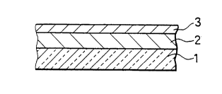
Fig. 1 is a cross sectional view showing the structure of an optical
memory medium according to one embodiment of the present invention.
Fig. 2 is a graph showing the absorption spectra of a compound
forming a recording layer of the optical memory medium when ring closure and
ring opening take place.
Fig. 3 is a graph showing the relationship between the temperature
and absorbance of the recording layer.
Fig. 4(a) shows the temperature distribution of a portion of the
optical memory medium exposed to laser light, and Fig. 4(b) shows a variation
in absorbance in the exposed portion.
The following description discusses one embodiment of the present
invention with reference to Figs. 1 through 4.
As illustrated in Fig. 1, an optical memory medium of the present
invention includes a transparent substrate 1, a recording layer 2 formed on the
transparent substrate 1, and a reflection layer 3 laminated on the recording layer
2.
The transparent substrate 1 is formed by, for example, glass or
plastic such as polycarbonate, and carries the recording layer 2 and the
reflection layer 3 thereon. The recording layer 2 on the transparent substrate 1is formed by dispersing a diarylethene derivative represented by the above-
mentioned general formula in a non-polar polymeric binder. The recording layer
2 thus formed is a photochromic medium and appears colored (i.e., ring closure
takes place) when exposed to shortwave light, while it becomes colorless (i.e.,
ring opening takes place) when exposed to visible light. In other words, the
recording layer 2 is isomerized to have different absorption bands.
The concentration of diarylethene derivative in the non-polar
polymeric binder is preferably in the range of about 0.1 to 50 weight percent.
For example, the recording layer 2 is a film with a thickness of about 0.1 to
.. . .
-
~P
6 2090 ~ 36
100 ,Lm, more preferably 0.1 to 10 ,um, formed by spin coating. The reflection
layer 3 is formed by a metal, such as aluminum and gold, by sputtering or vapor
deposition.
The above-mentioned description discusses only a basic structure
5 of optical memory media, and therefore the present invention is not restricted to
such a structure. An optical memory medium of the present invention may have
a different structure if it includes a recording layer 2 formed by the above-
mentioned diarylethene derivative dispersed in a non-polar polymeric binder. Forexample, it is possible to form a protective layer on the reflective layer 3 by an
10 ultraviolet light hardening resin, or to sandwich the recording layer 2 by
transparent dielectric films.
The two following experiments were performed to study the
photochromic properties of the recording layer 2 of the optical memory medium
ofthis embodiment. Specifically, 2-(1 ,2-dimethyl-5-methoxy-3-indolyl)-3-(2-cyano-
15 3,5-dimethyl-4-thienyl) maleic anhydride (hereinafter referred to as compound B)
of the general formula
~O\
0~, ~=0
C~O
C~
'~ S
C~
was dissolved in n-hexane, and shortwave light with a wavelength around 440
nm was then irradiated on the compound B so as to cause ring closure and give
color to the compound B. Next, a solvent was vaporized and mixed with non-
20 polar polymeric Zeonex 280* (produced by Nihon Zeon Kabushiki Kaisha).
*Trade-mark
'~
2090 1 36
Zeonex 280 is a polyolefin series plastic represented by the
general formula
R7 R~ /n
where R7 and R8 are C,Hm. The concentration of the compound B with respect
to Zeonex 280 was 0.5 weight percent. After dissolving the mixture in toluene,
5 the resulting mixture was deposited on a glass surface by casting, and then
baked at a temperature of 80C for three days so as to produce Sample a.
Sample a was exposed to shortwave light with a wavelength around 460 nm,
and the absorption spectrum was measured. The results are shown by the solid
curved line in Fig. 2.
10The absorption spectrum of the compound B in the colorless state
(ring is not formed) is shown by the broken line in the same figure. It was found
that, when Sample a was exposed to shortwave light with a wavelength around
460 nm, it had an absorption band different from the absorption band observed
when the compound B became colorless by the irradiation of light having a
15wavelength around 680 nm; the compound B appeared colored, or ring closure
took place. In other words, a significant photochromic change was observed.
Additionally, Samples b to e were prepared by dispersing the
compound B in PMMA (Mw = 12000, produced by Aldrich Chemical Company
Inc.), a polycarbonate resin (Mw = 14000, produced by Mitsubishi Chemistry
20Industry, Ltd.), and in polystyrene resins (Mw = 280000, 50000, produced by
Aldrich Chemical Company Inc.), respectively, and depositing them on a glass
surface in the same manner as when Zeonex 280 was used. Light with a
wavelength around 480 nm was irradiated on Samples b to e, and absorption
2090 1 36
spectra were measured. Photochromic changes were observed; however, these
changes were not as significant as that seen when Zeonex 280 was used.
The results show that, when the diarylethene derivative is dispersed
in the non-polar polymeric binder, it causes a significant photochromic change.
5 It is thus possible to provide an optical memory medium which fuliy utilizes
advantageous properties of diarylethene derivative, such as good thermal stability
of the colored state, durability against repeated color changes between the
colorless and colored states, and a photosensitivity to a semiconductor laser with
a wavelength of 780 nm.
10Next, in order to study variations of photochromism with respect to
changes in the temperature of the recording layer 2 formed by dispersing the
diarylethene derivative in the non-polar polymeric binder, the following
experiments were carried out.
First, to measure a change of absorbance with respect to light of
15a wavelength of 690 nm, light of a wavelength around 460 nm was irradiated on
Sample a, while the sample was heated on a hotplate. The results shown in Fig.
3 indicate that absorbance increases as the temperature rises, and the
absorbance changes significantly when the temperature exceeds 100 C. On
the other hand, when light of a wavelength around 460 nm is irradiated on
20 Samples b to e while the samples were heated to the vicinity of the glass
transition temperatures of the respective binder resins on a hotplate, only small
photochromic changes were observed.
It was discovered through these experiments that the recording
layer 2 of the optical memory medium of this embodiment has such properties
25 that, when the recording layer is heated to a predetermined temperature, it
shows a greater photochromic change in comparison with a photochromic
change at room temperature.
Meanwhile, when the laser light is irradiated on the optical memory
medium during recording of information, the region exposed to the light shows
30 (~ussi~n light intensity distribution. Consequently, when the intensity of the
recording laser light is set to a predetermined value, the exposed region has
2090 1 36
such a temperature distribution that only a portion corresponding to the center
of a beam spot has an increased temperature as shown in Fig. 4(a).
Therefore, when the intensity of the recording laser light is
controlled to irradiate a recording beam such that a portion of the recording layer
5 2 corresponding to the center of the beam spot has a temperature causing a
significant photochromic change, for example, 100C or above, the absorbance
of the recording layer 2 with respect to the visible light has the distribution shown
in Fig. 4(b) in the vicinity of the exposed region. As is clear from the figures, a
signiflcant photochromic change took place only at the central portion of the
10 exposed region of the recording layer 2.
It is therefore possible to record a bit which is smaller than the size
of a light spot of the recording laser light, enabling high-density recording.
Moreover, since the recording layer 2 shows a significant
photochromic change when heated to the predetermined temperature or above,
15 it is possible to perform non-destructive readout. More specifically, first, the
optical memory medium shown in Fig. 1 is fully exposed to visible light to make
the recording layer 2 colorless. Then, the recording layer 2 is caused to becomecolored by shortwave light of high intensity so as to record information thereon.
With this arrangement, even when shortwave light of low intensity is irradiated on
20 the recording layer 2 during reproduction, the temperature of an unrecorded
(colorless) portion is not significantly raised when compared to the temperaturerise during recording. Thus, photochromic change is hardly observed, and the
contrast between the recorded portion and the unrecorded portion is preserved.
This makes it possible to perform non-destructive readout, thereby preventing
25 deterioration of reproduced signals.
However, a more detailed study of the optical memory medium of
this embodiment reveals that the irradiation of shortwave light during
reproduction deteriorates the recorded portion, namely, a gradual change from
the colored state into the colorless state was observed. In order to perform
30 more satisfactory non-destructive readout with the present invention, for example,
~P
~090 1 36
it is effective to perform simultaneous irradiation of shortwave light and visible
light as disclosed in "Denshizairyo", September 1991, p. 123.
In this embodiment, firstly, the recording layer 2 was made
colorless by the visible light. High-intensity shortwave light was used for
5 recording, and low-intensity shortwave light was used for reproduction.
However, the recording, reproduction and erasure of information are performed
in the same way in this embodiment, by irradiating the light in the reversed
manner. In this case, the recording layer 2 is firstly caused to have c~t~r ~ the
high-intensity shortwave light. Next, it is turned into a colorless state by the10 visible light so as to record information thereon. Then, the information is
reproduced by the shortwave light or the simultaneous irradiation of the
shortwave light and the visible light. This method also enables high-density
recording and non-destructive readout.
The optical memory medium of this embodiment may be an optical
15 disk, an optical card, or an optical tape. For instance, in the case of an optical
tape, a flexible tape base is used instead of the transparerlt substrate 1. For the
material of the tape base, for example, polyethylene terephthalate may be used.
The invention being thus described, it will be obvious that the same
may be varied in many ways. Such variations are not~to be regarded as a
20 departure from the spirit and scope of the invention, and all such modifications
as would be obvious to one skilled in the art are intended to be included withinthe scope of the following claims.