Note: Descriptions are shown in the official language in which they were submitted.
~Q~~2~~
wo g2/o65~ pcrivs9vos~os
-1-
IMAGE S .
The present invention relates to an image
sensor, and more particularly, to a color image sensor.
It is desirable to control the exposure in an
image sensor such as a charge-coupled device (CCD). If
an image sensor receives too much exposure, the
resultant saturation and/or "blooming" destroys the
spatial information and linearity of the video signal.
If the exposure is too low, the signal-to-noise ratio
and dynamic range suffer. Ideally, the maximum
exposure is controlled to a point just below device
saturation. The exposure can be controlled by either
adjusting the source illumination (radiance), the
collection optics (the solid angle subtended), or the
time-duration of light collection (the integration
time) .
The integration time of CCD~s can be
controlled electronically. Typically, line time, i.e.,
the time between successive transfers of charge from
the photodetectors to the shift registers, and the
integration time are the same. However, there are
sensors which electronically divert the photodetector
charge to the substrate (so that no charge is
collected) during the first portion of the line time,
~ and then isolate the photodetector (so that charge is
collected) for the remainder of the line tame. This is
referred to as electronic exposure control or
electronic shuttering.
Electronic exposure control has been
previously used in monochrome linear CCD sensors.
There is a problem, however, in using electronic
exposure control for color image sensors. Integrated
color linear CCD sensors have taken two forms. In one
form, patterned cdlor filters (such as a repeating red-
green-blue pattern) have been placed on a single linear
. CCD. In another form, individual filters have been
placed on three linear CCD~s fabricated on a single
w
WO 92!06564 ~ ~ E~ ~ ~ ~ ~ PCTlUS91/069t?6
_2_
substrate. A problem in controlling the exposure in
both types of these sensors is that different colors
should receive different integration times. One reason
that different integration times are needed is that the
red green and blue filters do not transmit the same
photon flux in the pass bands for red, green, and blue,
respectively. Another reason is that the light sources
for scanners are not spectrally balanced; a tungsten
light source, for example, is heavily weighted in the
red.
One attempt at solving the problem of
providing the proper exposure for each of the colors in
a color image sensor is disclosed in U.S. Pat. No.
4,709,259, to Suzuki. This patent discloses a color
image sensor which has a matrix of photodiodes each of
which is adapted to sense red, green, or blue light,
Charge signals stored in the photodiodes are
transferred by means of MOS switches to three
horizontal shift registers, one for each of the primary
colors. Three vertical shift registers are provided to
turn on the MOS switches for each color, and the charge
storage time for each color is varied by varying the
operating times of the three vertical shift registers.
One of the main problems with the arrangement shown in
the Suzuki patent is that the three colors cannot be
clocked out in parallel, and thus, a complicated timing
arrangement is necessary in order to process the
signals.
It is an object of the present invention to
overcome the problems in the prior art discussed above
and to provide an improved color image sensor.
In accordance with the present invention,
there is provided an image sensor comprising: an array
of image sensor elements, each of the elements being
adapted to produce a color representation of a portion
of a color image, some of the elements being adapted to
sense a color different from other of the elements; and
WO 92/06564 ~ ~ ~~ ~ ~ ~ ~ PCT/US91/U6906
-3-
means for controlling the integration time of each of
the sensor elements in accordance with the color which
the element is adapted to sense.
In one embodiment of the present invention,
the image sensor comprises three channels, one channel
for each of the primary colors. Each channel is
identical except for the color of the filter which
overlies the image sensor elements. Each channel
comprises a line of photodiodes and an adjacent CCD
shift register. Charge carriers accumulated in the
photodiodes are transferred to the CCD shift register
through a transfer gate located between the photodiodes
and the shift register. A line of charge packets in
the shift register are then sequentially read out to an
output circuit. An exposure drain is located adjacent
each of the photodiodes, and an exposure control gate
between the photodiode and the drain controls the flow
of charge carriers from the photodiode to the drain.
The potential on the exposure control gate can be
controlled to control the effective integration time of
the photodiode. The integration time for each of the
channels can be different and is controlled in
accordance with the color being sensed by that channel.
The line readout time for each of the channels is the
same, however, and thus, all of the channels can be
read out in parallel.
One of the main advantages~of the present
invention is that an optimum exposure time is obtained
for each of the colors in a color CCD image sensor. A
further advantage is that a.common line time is
maintained in such a sensor for all three channels. A
still further advantage of the invention is that
blooming can also be prevented in such a sensor.
Embodiments of the present invention will now
be described, by way of example, with reference to the
accompanying drawings in which:
~0~~
WO 92/Ot564 PCT/US91/06906. .~
FIG. l~is a schematic plan view of the image
sensor of the present invention;
FIG. 2 is a plan view of one channel of the
image sensor;
FIG. 3 is an enlarged top plan view of a
portion of one channel;
FIG. 4 is a sectional view taken along line
4-4 in FIG. 3;
FIGS. 5 and 6 are timing diagrams
illustrating the operation of the present invention;
FIGS. 7 is a timing diagram showing the
integration times for each colar in an illustrative
example of the present invention; and
FIG. 8 is a schematic diagram of circuitry
for generating timing signals for the image sensor.
The present invention is described herein
with reference to an image sensor which comprises a
plurality of image elements, each of the elements
including a photodetector, a CCD, a drain, and the
appropriate transfer gates. The present invention can
also be used with other types of image sensors, for
example, image sensors in which the elements include an
accumulation region, and the charge carriers are
transferred from the photodetector to the accumulation
region and then to the CCD. Further, the image sensor
is described as a tri-linear sensor in which individua l
color filters are placed over three linear arrays;
however, the invention is equally applicable to a
single linear array with a patterned color filter in
which a separate transfer gate is available for each
cell.
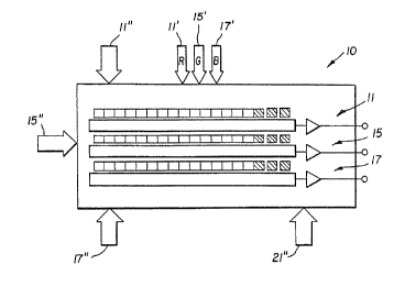
With reference to FIG. 1, there is shown a
schematic view of an image sensor 10 constructed in
accordance with the present invention. Image sensor 10'
comprises a red channel 11, a green channel 15, and a
blue channel 17. As will be explained in more detail
hereinafter, independent signals 11', 15', and 17' are
WO 92/06564 ~ ~ ~ ~ ~ ~ 5 PCT/US91/06906
-5-
provided to the channels for exposure control, and
independent clock signals 11 " , 15 ", and 17 " are
provided to the channels for readout of the sensor.
Common detector-to-shift register clock signals are
provided to sensor 10, as indicated by arrow 21. Image
sensor 10 can be used in a device, such as a film
scanner, to record electrica:L signals representative of
a color image.
Each of the channels 11, 15, and 17 is
constructed as shown generally in FIG. 2 and in more
detail in FIGS 3 and 4. Each of the channels 11, 15,
17, is identical, except for the color filter (not
shown) used in the channel; thus, only channel 11 will
be described in detail. Channel 11 comprises a
substrate 12 having a major (top) surface 14.
Substrate 12 can be made from a semiconductor material
such as p-type single crystalline silicon. A line of
photodetectors 16 are disposed in substrate 12 along
the major surface 14. Extending adjacent each line of
photodetectors 16 is a CGD shift register 18. Between
each photodetector 16 and shift register 18 is a
transfer gate 26. On an opposite side of the
photodetectors 16, exposure drain 22 extends along and
substantially parallel to the line of photodetectors
16. An exposure control gate 30 extends along the
space between the line of the photodetectors 16 and the
adjacent exposure drain 22.
As shown in FIG. 4, each photodetector 16 is
a photodiode of the type which includes an n-type
conductivity region 34, (shown as n) in the substrate
12 at the major surface 14. Typically the conductivity
of region 34 is about 101 impurities/cm3. The
substrate 12 is preferably of p/type conductivity
(shown as p-), typically of 1015 impurities/cm3, or it
can nave a p-type well in the surface 14 of an n-type
conductivity substrate in which the photodiode is
formed. A second, highly conductive, p-type
WO 92/06564
PCT/iJS91 /06906
_5_
conductivity region 36 (shown as p+), typically of a
conductivity of 1018 impurities/cm3, exists within a
portion of the first region 34 at the substrate surface
14. Regions 12, 34 and 36 form a pinned, or buried,
diode. However, instead of the photodiode 16 shown,
any other known type of photodetector can be used, such
as a Schottky barrier photodiode or a simple pn
junction diode.
The CCD shift register 18 may be of any well
known construction. A buried channel configuration is
shown in FIG. 4. The shift register 18 comprises an n-
type conductivity channel region 38 (shown as n-) of
impurity concentration of about 101 impurities/cm3 in
the substrate 12 at the surface 14. The channel region
38 extends along the surface 14 spaced from and
parallel to the line of photodetectors 16. Over the
channel region 38 are a plurality of conductive gates
40 and 41 (FIG. 2) which are spaced along the channel
region 38. The gates 40 and 41 can be made of a metal
or conductive polycrystalline silicon, and the gates
are insulated from the substrate surface 14 by a layer
43 of a dielectric, typically silicon oxide. The gates
40 and 41 are connected to a potential source by means
of bus lines dl and d2 (FIG. 2) for selectively
applying a potential to the gates to operate the shift
register 18.
The exposure drain 22 is formed by a region
46 of n.+ type conductivity (shown as n+) and of a
conductivity of about 1019 impurities/cm3 in the
substrate 12 and extending to the surface 14. The
region 46 extends along the entire length of the line
of photodetectors 16 and is spaced from the
photodetectors. The drain region 46 is connected to a
source of potential (not shown) through a conductive
contact 48.
Each of the gates 26 and 30 is a strip of a
conductive material, such as a metal or conductive
WO 92/06564 ~ ~ ~ PCT/US91/06906
polycrystalline silicon, which is on the silicon oxide
layer 43. The transfer gate 26 extends over the space
between the shift register 18 and the line of
photodetectors 30 and overlaps the shift register gates
40. ,The transfer gate 26 is insulated from the shift
register gates 40 by a layer. 54 of silicon oxide which
covers the shift register gates 40. The exposure
control gate 30 extends across the space between the
exposure drain region 46 and the line of photodetectors
16 along the full length thereof. The exposure control
gate 30 overlaps the exposure drain region 46.
In the conventional operation of an image
sensor of the type described herein, charge carriers
are allowed to accumulate in photodetectors 16.
Raising and then lowering the potential of transfer
gate 26 causes the charge accumulated in the
photodetectors 16 to be transferred into shift register
18 in a manner well known in the art. The line of
charge packets in the shift register 18 are then
sequentially read out. At the end of the readout for
one line, the next line of charge is again transferred
from the photodiodes 16 into the shift register 18.
The integration time (i.e., the time that charge is
allowed to accumulate) is thus equal to the line
readout time (the time between successive transfers of
charge) .
In the present invention, the potential on
the exposure control gate 30 is controlled to adjust
the effective integration time to be less than or equal
to the line readout time. Raising the potential on
exposure control gate 30 causes the photo-induced
charge normally accumulating in the photodiodes 16 to
be transferred into the exposure drain 22 where it is
removed by externally-applied bias. Lowering the
potential on exposure control gate 30 isolates the
photodiodes l6 allowing photo-induced charge to
accumulate in the normal manner. It will be seen that
2~~~~?'~
WO 92/06564 PCT/US91/06906
_g_
by coordinating the timing of the exposure control gate
30 and transfer gate 26, the integration time can be
adjusted to a fraction of the line readout time, This
process is known as electronic shuttering.
The timing required to ogerate image sensor
in order to control the integration time for a
channel is shown in FIGS. 5 and 6. As shown_ in FIG. 5,
the potential on exposure control gate 30 is raised
with the falling edge of the potential on transfer gate
10 26 (the beginning of a line period?, and is lowered at
the desired point (indicated at 60) in the middle of a
line period Tline~ Consequently, the integration time
Te,~p is the period from the falling edge of the
potential on exposure control gate 30 to the next
falling edge of the potential on transfer gate 26.
Independent exposure control gate lines are provided to
each of the channels, and thus, the integration time
2e,tp can be independently varied for each color while
maintaining a constant line time Tline~
The photodiode to CCD shift register timing
is shown in FIG. 6. Transfer of charge carriers from
the photodetectors 16 to shift register 18 occurs
during the time Tpd. The period 'ttg is required to
allow charge carriers under the transfer gate 26 to be
cleared into the shift register 18. It will be noted
that the falling edge of the potential on exposure
control gate 30 is also shown to be coincident with the
rising edge of the shift register clock signal t~2. The
coincident timing is preferred to minimize switching
artifacts on the sensor output, which might distort the
image signal.
The signals necessary to operate image sensor
10 in accordance with the present invention can be
provided by any appropriate commercially-available
logic devices. In one illustrative example of the
present invention, the relative integration times for
the red, green, and blue channels could be 1/4, 1/2,
WO 92/06564 ~ ~ ~ ~ PCT/US91/06906
_g_
and 1, respectively. FIG. 7 shows the timing pulses
11', 15', 17' for the red, green, and blue exposure
control gates. The effective integration time ~e~p is
also indicated. An example :is shown in FIG. 8 of the
control logic required to generate signals 11', 15',
and 17', as well as the transfer gate timing pulse TG
26'. A master clock 71 cycles at the desired CCD
readout rate. An 11 bit counter 73 feeds 11-bit
decoders shown in blocks 74. The decoders set or reset
R/S flip flops 75 at the appropriate counts,
Implementation of the arrangement shown in FIG. 8 can
be performed in conventional logic devices or can be
embedded in programmable logic.