Note: Descriptions are shown in the official language in which they were submitted.
PIIN 13996 1 ~ 16.06.1992
CMOS integrated circuit.
The invelltioll relates to a CMOS integrated circuit comprising a
semiconclllctor body with a layer-shaped region of substalltially a first conductivity lype
adjoining a surface, in which region an electric circuit is provided having at least two
adjacent circuit blocks separated from one another by an intermediate region and formed
5 in part;cular but not exclusively by rows of standard cells, which circuit blocks are built
up from MOS transistors having a channel of the second conductivity type and provided
in the layer-shaped region of the first conductivity type and from MOS transistors
having a channel of the first conductivity type and provided in surface regions of the
second conductivity type, called first surface regions hereinafter, while the surface is
10 covered with an electrically insulating layer on which a wiring pattern is provided
comprising a supply line and one or several signal lines provided above the interme(iiate
re~ion.
An integrated circuit realised with stcmdard cells is described inter alia in
15 the book "Geïntegreerde MOS-schakelingen, een inleiding tot ~TLSI en ASIC's"
(Integrated MOS Circuits, an Introduction to VLSI and ASICs) by H. Veendrick, ~1990)
Delta Press BV, Amerongen, the Netherlands, in particular pp. 376-77. The standard
cells may have various kinds of logic gates which may all have the sarne height. The
cells are arranged in rows which are mutually separated by transistorless interspacings
20 which are used as wiring channels. In the wiring channels, conducior tracks are formed
which interconnect the cells so as to guide signals from one cell to another cell. The
width of the wiring channels may vary in dependence on the quantity of wiring. The
supply lines are usually laid immediately above the cells, but sometimes they are
provided in the wiring channels.
25 Noise superimposed on the supply may form a major problem in large integratedcircuits. This noise may be caused, ~or example, by switching of certain elements, for
PHN 13996 ~ 7 ~ 16.06.1992
example flipflops in particular when more elements switch sirnultaneo-lsly whereby
locally considerable c~lrrents ancl tllus high voltage peaks occur in the sllpply lines.
~nother source of noise may be tormed by heavily loaclecJ Olltpllt stages. Tl~e peak
cllrrents in the snpply n~ay callse volt lge cl1 lllges in the circuit whicll aclversely affect
arlllleters sucll as for example speed and reliability. Cana(lim l'atent l 204 511
l~rnposes to reclllce supl)ly noise by means of decollpling capacitances which are formed
by a local capacitor consisting of a reverse-biasecl pn junctioll which is connected lo the
supply. This capacitor requires additional space so that the crystal becomes larger and
the circuit accordingly becomes more expensive. In addition it is often desirable to lay
l0 the decoupling capacitor even closer to the elements causillg the said current peaks than
in this known circuit.
It will be clear that the problems described above will not occur in
standard cells only. The present invention offers a solution to these problems in circuits
which are built up in blocks which blocks comprising circuit portions are provided in a
15 more or less regular pattern on the chip mutually separated by routing channels.
The invention has tor its object to provide a device of the kincl mentioned
in the opening paragraph in which a maximum decoupling capaeitance is obtained
without requiring additional space. Another object of the invention is to position the
20 decoupling capacitance as close to the elements as possible so that the current pealcs are
practically purely local and have no or subst~ntially no erosstalk to other portions of the
circuit.
According to the invention7 a CMOS integrated circuit of the kind
described in the opening paragraph is characterized in that the layer-shaped region of
25 the first conductivity type is provided with one or several additional surface regions of
the second conductivity type at the area of the intermediate region below the signal
lines which regions are electrically connected to the supply line. Since the space in the
semiconductor body below the wiring channels is generally not used for circuit
elements the provision of the additional decoupling capacitance below the wiring30 channels requires no extra space which would lead to an increase in the surface area.
Thanks to the invention in addition the decoupling capacitance can be positioned at a
very small distance from the switching elements.
3 ~
Pl-~N 13996 3 16.06.1992
,'\ special embodiment, whicll has the advantage that the additional
surfilce regions can be provide(l simllltalleollsly with ~he saicl first surface regions, is
characterized in that the additional surface regiolls h.lve a sanlc thicklless ancl doping
concelltration as the first surf~ce regions in which the MOS transistors with channels of
the first con(lllctivity type are provide(l. A r~lrther embodilllent of a device according to
the invclltioll, in whicll no separate contacts are necessary ~or the additiollal surface
regions, is characterize~l in that at least one of the additional surface regions together
witll at least one of the first surface regions forms a coherent surface zone of the second
conductivity type. ~ further embodiment, in which a further increase of the deco~lpling
10 capacitance is obtained without an increase in the surface area of the serniconductor
body, is characterized in that the supply line is connected to a contact pad through a
conductor track which is situated next to the circuit blocks, the layer-shaped region of
the first conductivity type being provided with a surface region of the second
conductivity ty~e below this conductor track, which surface region is connected to the
15 conductor track.
The invention will be explained in more detail with reference to a few
embodiments and the accompanying diagrammatic drawing in which:
Fig. 1 is a dia~rammatic plan view of an integrated circuit with standard
20 cells according to the invention;
Fig. 2 shows a portion of Fig. 1 on an enlarged scale;
Fig. 3 is a cross-section of a portion of the device of Fig. 2; and
Fig. 4 is a plan view of a portion of an integrated circuit according to a
second embodiment of the invention.
It is noted that the drawing is only diagrammatic and that the various
components of the circuit are not depicted true to scale.
The device of Figs. 1-3 shows a CMOS integrated circuit I with a
semiconductor body 2 of, for example, silicon or a different suitable semiconductor
30 material. The semiconductor body comprises a layer-shaped region 4 of substantially a
first conductivity type, in the present example the p-type, adjoining the surface 3. The
circuit provided in the layer-shaped region 4 is built up from standard cells. Such
PHN 13996 4 16.06.1992
s~andard cells may comprise various gates, for example, logic gates such as inverter
circuits, AND gates, OR gates, etc., or gates such as flipflops, which are usllally
~vailable to tlle clesigner in a so-called library dllring the design of an in~cgrated circuit.
The cells in the present example have the same height (dimensi()rl in thc y-direction);
~he lengths ot the cells (climensioll in the x-direction) depen(l on, for e~aml)lc, ~he
mllllbel of componellts in the cell an(l may be mutllally differellt. Tl1c cells ~re arral1ge(1
one after the other to form rows 5 which extend in the x-direction; the rows, whicl1 may
be of different lengths, are laid next to one another in the y-direction. Fig. 1 shows
only three rows 5, but in actual fact the number of rows will usually be much greater.
10 Above the surface, and separated from this surface by an insulating layer 6 of, for
example, silicon oxide, a wiring pattern 7 in the form of conductor tracks is provided.
Apart from supply lines, which will be discussed further below, the wiring pattern
comprises signal lines for passing on electrical signals to the standard cells and from
one standard cell to another, possibly in the same row, possibly in another row 5. The
15 signal lines 7 are provided in intermediate regions 8 between the rows 5 whicl1 serve
only to accommodate the wiring and which are empty for the rest, i.e. contain nocircuit elements such as transistors. The intermediate regions 8 will also be called
wiring channels or routing channels in the following description. The supply lines 9 and
10 depicted in Fig. 2, to which the positive voltage V~l or the reference voltage V, can
20 be applied during operation, may also be provided in the routing channels 8, but in the
present example they are laid immediately above the standard cells in the rows 5.
The standard cells comprise complementary MOS transistors of which Ihe
p-channel MOST 11 and the n-channel MOST 12 are drawn in Fig. 2. The transistors11 and 12 form, for example, an inverter in which an input signal is supplied to the
25 interconne~ted gate electrodes and the output signal is derived from the interconnected
drains; the sources of the transistors 11 and 12 are connected to the positive supply line
9 and the negative supply line 10, respectively. Obviously, further circuit elements may
be present in the cell drawn in Fig. 2. The transistor 11, with p-type source and drain,
is provided in a surface region 13 of the conductivity type opposite to that of the
30 substrate 4, so of the n-type. Surface regions 13 are usually designated as "wells" or as
"pockets" in the literature. The n-channel ~IOST 12 with n-type source and drain zones
may be formed directly in the p-type substrate 4 in known manner.
PH N 1 3996 5 1 6 . 06.1 99
At tlle area of the intermediate regions 8 between the rows 5 of standard
cells and below the wiring 7, according to the invention (l~ig. 2), the layer-shaped
rcgion or substrate 4 of the p-type is provide(l with one or scveral a(l(litional surt`ace
regions 14 of lhe n-type which are electrically connectcd to the supply linc 9. This
S ~td(litional region 14 is in(licclte(i with a dot-(lilsll line in l ig. ~. OwinL~ tO lhis region, a
large ad(litional capacitance t`ornle(l by the pnjllncliol) between the substrale ~ and the
n-type zone S is connecte(l in parallel to the supply line 9, acting as a buffer in the case
of klrge local current peaks, so that voltage fluctllations in the line 9 are redlJce(l. The
surface region 14 may be forrned at any n-type doping step in the process. For reasons
IQ of process technology, however, it is most convenient to provide the zone 14
simult~neously with the well 13, so that the region 14 has the same thickness and
doping concentration as the well 13. The region 14 and the well 13 form a continuolls
n-type zone, so that the connection between the supply line 9 and the zone 14 isobtained through the well 13 which, in usual manner, is connected to the line 19 at the
15 area of the contact 16.
Fig. 1 shows, besides the rows 5 and the routing channels 8, a number of
contact pads 17 along the circumference of the integrated circuit for the fastening of
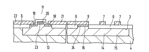
wires. The cross-section according to Fig. 3 shows from left to right a p-cllallnel MOST
11, with a p-type source and drain 18 and 19, respectively, formed in the n-type region
20 13 and wi~h a gate electrode 20. The source 18 is connected to the supply line 9
through a conductor 21, and to the n-type well 13 through the supply, while the drain
19 is connected to the conductor 22 through which the drain 19 can be connected to the
n-type drain, not shown in Fig. 3, of the transistor 12. The gate electrode 20 is
separated from the transistor channel by the thin gate oxide 23. To the right of the
25 transistor, Fig. 3 shows the connection 16 between the supply 9 and the n-type well 13,
with the n-type cont~ct zone 24 in the opening 16 in the field oxide 6. The n-type well
13 then merges into the additional n-type region 14 which provides the extra decoupling
capacitance for the supply, as described above. The region 14 is covered with a thick
oxide layer 6 on or above which the conductor tracks 7 of the wiring channels are
30 proYided.
The device may be manufactured in a manner which is generally known
per se, familiar to those skilled in the art, and which is not explained in any detail here.
2~ r~
PHN 13996 6 i6.06.1992
In a specific embodiment the height of the standard cells was approximately 70 um
while the height of the n-well 13 was approximately 35 ~111. The width of the routing
chlnncls i.e~ the interspacing bctween the rows 15 in ~his embo(iiment~ vas alsoapproxil~ tely 7n ~Im~ By filling this inlersl-lcing with the ad(litional region 14 it is
ossible to make the dccollpling capacit.lnce practically ~hlce linles ~llat of a s~alldar(l
vcll. ~ stan(lar(l cell with an inverter wllose length (dimension in the x-dir~ctioll) in lhis
specific embo(linlellt was approxirmately 12.8 ~m yielded an a(l(lition ll decollpling
capacitance of approximately 140 fF in the manner described above. ~ flipflop cell with
a length of approximately 76.8 ~lm yields an extra decoupling capacitance of
10 approximately 845 fF. These large capacitances are obt~ined without an increase in the
surface area of the semiconductor body and without changes in the process. A ~ery
important aspect of the invention is that the decoupling capacitances are situated
immediately adjacent the current-conducting circuit elements so that the current peaks
arising through switching of the elements are practically only local and have no or
15 hardly any crosstalk to other portions of the integrated circuit.
F;g. 4 is a diagrammatic plan view of a portion of a seconcl embodiment
of an integrated circuit according to the invention. Corresponding components in Fig. 4
have the same reference numerals as in the first embodiment. The circuit again
comprises a number of rows S of standard cells of which three are shown in the
20 drawislg. The rows S are mutually separated by routing channels 8 the wiring being left
out again for reasons of clarity. Decoupling capacitances in the form of wells 14 are
provided below each of the routing channels in the same maulner as in the preceding
embodiment.
rhese capacitances are shown as a continuous zone in the drawing but it
25 will be obvious that this is not necessarily the case and that a separate well 14 may be
formed for each standard cell. The supply lines 9 are connected to a contact pad 17
through a compara~ively wide conductor track 25 which extends substantially
transversely to the longitudinal direction of the rows S over the surface of the de~ice.
The track 26 may be formed in the .same wiring layer as the conductor tracks 9 but is
30 often provided in a different metal layer. To obtain a further increase in the decoupling
capacitance of the s~lpply lines an n-type surface region 27 indicate~l with a dot-dash
line in the drawing is provided below the conductor track 26 in the p-type substrate.
r~
PHN 13996 7 16.06.1992
The conductor track 26 is connected to the region 27 at the area of contacts 28. The
zone 27 may form a single continuous region, but it may alternatively be subdivi(led, as
shown hl ~he clrawing, into a nlllllber o~ partial regions eacll connecte(l to the con(lllclor
track ~6. The region 27 may be manllfact-lre(l simllltalleo~!sly with the regions 14 an(l
~vi~h the n-type well of lhe cells. An important furtller increase in the decollplillg
capaci~ance is obtailled in this mallner without an enlargement of the circuit, because the
spaee below the track ~6 is not used anyway for providing switching elements.
It will be obvious that ~he invention is not limited to the embodiments
described here, but that many variations are possible to those skilled in the art within
10 the scope of the invention. Thus the conductivity types in the examples described may
be interchanged, so that the substrate 4 is of the n-type and the well 13 and the
aclcJitional region are of the p-type. The polarity of the voltage between the sl~bstrate and
the regions 13-14 shoul~l then also be inverted, of course. Apart from MOS transistors,
different cireuit elements, such as bipolar transistors, resistors, eapaeitors, diodes, ete.,
15 may be ineluded in the eircuit. The invention is applicable in eireuits for both digital
and analog and mixed analog/digital funetions. The invention is not limited to circuits
comprising standard cells, but may also be used in circuits with eustom layout blocks
and routing ehannels between the bloeks.