Note: Descriptions are shown in the official language in which they were submitted.
~092/0~692 PCT/GB91/01525
1 2~9~
8EC~RIT~_DEVICB
The invention relates to security devices, methods for
constructing such devices, and methods and apparatus for
authenticating the devices.
5Security devices such as holograms and diffraction
gratings have become well known for protecting
identification articles such as credit cards and the like.
A typical example is described in US-A-4269473 in which a
hologram is incorporated into a layer of an identification
card. In this case the hologram includes machine
readable characters as well as a visual reprèsentation of
the other features of the card.
US-A-4l84700 describes the provision of a relief
structure on a thermoplastic coating of an identification
card or document which responds to incident, visible light
to generate an interference pattern.
US-A-4544266 describes a special diffraction pattern
which is provided on an identity card or the liXe, the
pattern comprising for example a hologram or diffraction
grating. The diffraction pattern will diffract light at
different wavelengths in different directions and this is
used to provide an indication of whether a security device
under test is authentic.
US-A-3542448 discloses the recording of a number of
holograms in different sub-areas of a storage medium so
that upon exposure to light, coded information within the
holograms can be determined.
GB-A-2016775 describes the provision of two optical
markings on a substrate which cause a reading light be to
deflected in different directions.
US-A-41403?3 describes a composite hologram which
generates two machine readable codes which can be read at
respective, different wavelengths. This suffers from the
disadvantage that the existence of machine readable
information is readily apparent and thus is likely to be
fraudulently copied.
W092/04692 ~ PCT/GB91/01525
~9~ 43~
There is a continuing need to increase the security of
devices of this type and in accordance with a first aspect
of the present invention, we provide a security device
comprising first and second diffractive structures
contained within a surface relief structure, the structures
being such that the device responds to illumination at a
first, visible wavelength to generate a first, visible
pattern while any pattern generated by the second structure
is not substantially visible at that wavelength, and that
the device responds to illumination at a second wavelength
substantially different from t~e first wavelength to
generate a second pattern suitable for machine reading
while any pattern generated by the first structure is
substantially suppressed.
This new security device involves the provision of
first and second diffractive patterns to form a composite
structure, which patterns are individually generated (eg.
reconstructed) upon illumination at two different
wavelengths and alternately predominate dependinq upon the
wavelength of the incident radiation used for
reconstruction of the images.
This device appears to the normal observer to be
conventional in that the first pattern is visible (ie.
human readable) upon normal illumination. It has enhanced
2~ security not only because of the presence of the second
structure but also because the machine readable pattern is
not apparent upon illumination with the first wavelength.
Typically, at the second wavelength the first
structure pattern is angularly or spatially separated from
the first pattern.
The patterns may be fully superposed (ie. added to
form a single, combined relief structure), partially
overlap, or be positioned side by side.
In one example, the second wavelength may comprise
infra-red radiation and the first wavelength may be a band
of white light, ordinary lighting or monochromatic
radiation. The references to illuminat on at first and
W092/04692 PCT/GB91/01525
3 2~9~?~
second wavelengths includes illumination at first and
second wavelength bands. In this context, visible
wavelengths are regarded as lying in the range 400 nm to
700 nm~ Usually, the second wavelength will be longer
s than the first and preferably will lie in the infrared
range, particularly the near infrared. Typical
wavelengths for the second wavelength will be in the range
701 to lO00 nm, preferably 850 to 950 nm.
In the preferred example, a wavelength of about 950 nm
will be used with a small band o~ radiation centred around
that value. Alternatively, an even narrower band such as
generated by a laser for example a solid state laser diode
could be used.
Effectively, this new security device enables the
lS second pattern to be substantially concealed from the user
of a security printed document, card or other substrate on
or verifiably within which the device is provided. This
concealment can be enhanced at the first wavelength if the
second pattern has a lower brightness than the first
pattern (eg. less than 20%), or is at a substantially
different angle, or is reconstructed at a different
distance from the first.
one example of the first structure would be one which
generates a "rainbow" (Benton) display hologram made by
conventional embossing and metallising for visual
authentication overlaid with a second structure for
generating a weak machine readable diffraction grating or
hologram, the second structure covering the entire area of
the first and designed to be read at infra-red wavelengths.
Upon illumination with white light a rainbow hologram will
reconstruct to give an image banded with colour especially
visible at the peak of the eye response (500-600 nm), the
colour changes depending on the viewing angle.
Another method for concealing the second diffractive
3S pattern upon irradiation at the first wavelength is to
arrange for the image forming the second pattern to be
formed (ie. reconstructed) much further from the device
w0~2/04692 PCT/GB91/01525
3~ 4
than the image from the first diffractive structure.
Indeed, preferably the second reconstructed pattern is
formed at a relatively far distance from the device, for
example between lO0 mm and 300 mm. This maximises the
S blur associated with the image generated by the second
structure under white light viewing conditions due to
chromatic aberrations resulting from dispersion.
Typically in a visual rainbow hologram, image points
greater than 50 mm from the image plane (ie. the surface of
the device) become blurred due to chromatic aberrations
because of dispersion. If the machine readable feature
forms an image at points further, possibly much further,
from the image plane than this (200 mm to 300 mm) then
there will be a large degradation in the image formed of
the machine readable feature under normal lighting
conditions making visual detection of the machine readable
feature very difficult.
Preferably, the first and secon~ diffractive
structures extend over substantially the same area of the
device.
However, the rainbow hologram and machine readable
feature could also occupy different regions of the dèvice.
For example the machine readable structure may be
incorporated in part of a standard image hologram design,
either added to it or surrounded by it.
A typical example would be a display hologram
containing a visually verifiable and distinctive first
image plus a concealed machine readable second image.
This would be used as a security device for the
authentication of documents, financial cards (such as
credit cards, bank notes) or goods, by providing a brand
protection label etc., as a security feature against
counterfeiting and forgery with both visual and covert
machine readable security. The device may also be
incorporated in a passport, visa, identity card or licence.
Optionally the information in the machine readable image
could vary from the visual image (e.g. batch encoded over
~V092/0~692 PCT/GB91/01525
5 2 0 ~ 3 g
a small number of variations) for use as an additional
security feature for example for t~e decoding/verification
of credit cards in ATMs (automatic teller machine).
The advantage of recording the ~econd diffractive
structure over the same area as the first is to prevent any
particular area of the display image looking noticeably
different or degraded and to enable the whole area of the
security device to contribute to the second reconstructed
pattern so increasing its relative brightness on readout.
It is also possible, however, by careful aesthetic
design to include the white light hologram wholly or partly
within the area having the machine readable diffraction
pattern, or to confine the machine readable portion to a
small area within or abutting the white light hologram.
This can be disguised by good design.
The machine readable area will generally not be less
than l square millimetre in area.
The hologram and the machine readable portion may
abut. Thus for example a thin ribbon for exhibition on an
authenticatable item may comprise adjacently embossed
regularly repeating abutting hologram and machine readable
diffraction pattern features~
While it is generally preferred that the two
structures will at least overlap it is possible for the
structure to be spaced by a small area of plain metal.
Commonly reconstructed images from both diffractive
structures will be viewed by reflection in a conventional
embossed hologram arrangement.
In another method the first and second diffractive
structures are designed such that at the readout
wavelengths of the second, machine verifiable structure
(preferably near infrared wavelengths) the first order
diffracted beam from the first diffractive structure is
diffracted within the body of the device i.e. below the
horizon tor plane) of the device. That is the first order
diffraction angle is at least 90 This means that the
image generated from the first structure upon illumination
W092/04692 PCT/GB91/01~25
~9~ ~36 6
at the second wavelengtbs effectively does not exist at
these wavelengths, so considerably enhancing the signal to
noise ratio on readout for the machine verifiable
structure.
Furthermore, it enables the pattern generated from a
very weak machine readable diffractive structure to be
concealed by the reconstruction from the visual first
diffractive structure upon illumination at the first
wavelengths but yet to be reconstructible with good signal
to noise ratio for machine verification at infrared
wavelengths.
There are two main advantages in eliminating the
reconstruction from the first pattern when illuminating at
the second wavelength. Firstly, there is no angular
overlap of the various reconstructed elemen~s that
constitute the first and second pattern generating
structures so that, in the case of the first diffractive
structure being a visual hologram, the "Benton" slits will
vanish under the horizon, which leaves in principle an
almost unrestricted angular space into which the second
pattern ~an reconstruct a machine verification pattern.
The second advantage follows from the fact that it is
important to limit the a~plitude of the second structure
and therefore its diffraction efficiency or brightness so
that in general the reconstruction from the second
structure will be much weaker than that from the first to
improve invisibility~
The first diffractive pattern can take a variety of
forms of a conventional nature such as object holograms,
two dimensional graphical diffraction effects, combined two
and three dimensional graphical diffractive patterns,
single or matrixed diffraction gratings, computer generated
interference patterns, kinegrams, stereoholograms and the
like. The term "hologram" is used generically to include
these. White light viewable holograms of the rainbow or
Benton types are preferred as the first diffractive
structures. Preferably, diffractive d~vices are used
WO 9~/0~1h9~ PCT/GB91/01525
7 2090~
which reconstruct to provide images which give a perception
of depth, such as images of three dimensional objects, and
graphical diffraction patterns which give the perception of
there being a numher of planes of depth on which images are
represented~
The preferred types of three dimensional images will
reconstruct to give the impression of the image being
located at a position intersecting or close to the
(physical) plane of the device. The i~age is percaived to
be confined within parallel planes to the surface set at
typically no greater than 50 mm on either side of the true
surface.
Such images which are being groupe~ under the generic
name "holograms'` may be created by holographic recording on
an optical bench using a coherent laser light source. It
is however possible to create simple diffracting patterns
by mechanical ruling methods.
Alternatively diffractive patterns of a complex nature
can be created by creating an instruction set in a computer
which is then used to drive a fine electron beam which
causes a surface relief pattern to be created on the resist
coating exposed to the beam.
The second structure may also have a conventional form
as above or it may consist of an image hologram of an out
of plane image consisting of a coded pattern of discrete
spots. For example, a set of image points forming a
digital e.g. on/off pixel pattern is particularly useful.
This image is simply formed by a series of diffracting
beams emanating from the device on illumination and thus
not necessarily having ~o reconstruct to form an image.
In other words, the coded pattern can be regarded as a
picture of a series of blocks. In this case an image of
the blocks would be reconstructed. The alternative way is
simply to create a set of beams which would diverge, these
beams forming the coded pattern.
W~92/04692 PCT/GB91/01525
~`~9~ 8
This machine readable pattern will generally be
recorded on the holographic table while making a white
light hologram.
In accordance with a second aspect of the present
invention, a method of constructing a security device
according to the first aspect of the invention comprises
forming the first diffractive structure as a surface relief
on a substrate; and forming the second diffractive
structure as a surface relief in the same region of the
substrate as the first structure~ Both ætructures
preferably combine to form a single surface relief pattern.
The first and second pattern generating structures may
be formed simultaneously or sequentially.
~ or example, the manufacturing technique can utilise
conventional holographic origination for display holograms
preferably recorded onto photoresist which can then be used
to form embossing shims for the mass production of embossed
bolograms. The final photoresist hologram or "H2" can be
recorded by conventional transfer from one or more rainbow
"Hl" holograms to form the visual display image, plus
exposure to either a diffusing target to give a pixel
pattern, or whatever other form of machine verifiable image
is desired. Thus, after recording of the first and
second structures into a photoresist coating, the coating
will be developed to provide the surface relief pattern
which will eventually be used for embossing. This
pattern will be electroformed into nickel and further
replicas will be made for use on the embossing machine.
We refer to "embossing" but replication of the surface
relief pattern could occur by using the polymerisation
methods of replication well known for use with holograms.
After replication the transparent polymeric surface
will be metallised such as with aluminium or another
suitable metal. This metallisation may be full or
partial. Partial metallisation may be through the use of
a very thin but even coating of metal. Alternatively the
W092/0~692 PCT/GB91/01525
209~3~
creation of a halftone-like pattern of metal may be
employed as known in the art.
As an alternative to metallisation after embossing it
is possible to emboss a thinly metallised surface.
The polymeric surface which is embossed will generally
be in the form of a plastic film or plastic coating
supporte~ on a substrate having a smooth surface~ Lacquer
coated paper, optionally containing release agents, may be
employed but generally the optical quality of the image is
inferior to that found with smooth plastic film. This
lac~uer coated paper may be metallised after embossing and
treated with a polymeric protective lacquer.
Alternatively the lacquer may be metallised before
embossing. Metallisation may be achieved by vapour or
otherwise coating with a thin metallic layer such as
aluminium, chromium or copper Alternatively, a thin
layer of a different diffraction effect enhancing layer
which has a refractive index different from that of the
transparent polymeric material in use may be employed (such
20 as described in US-A-4856857).
Examples of such are:
Transparent continuous thin films having a greater
refractive index than the polymeric material comprising the
diffractively embossed surface such as titanium dioxide,
zinc oxide, zirconium oxide, silicon oxide, magnesium oxide
and the like.
Transparent strong dielectrics having a refractive
index greater than that of the polymeric material such as
barium titanate.
3~ Transparent continous thin films having a smaller
refractive index than the polymeric material such as
magnesium fluoride~
organic polymeric coatings which have a significantly
different refractive index to the polymeric materials such
as poly vinyl butyryl, polyethylene, polyvinylchloride and
the like.
W092/0~69~ PCT/GB91/01525
~9~ ~3~
In a preferred arrangement, the second structure is
formed by exposing the substratè to a recording beam
through an aberrating optical system.
This leads to an increase in security~ If a set of,
for example cylindrical or highly aberrated ~but
reproducible) optics or mirrors is used during the original
recording a similar set of optics would be required within
the reader to enable an i~age of the original machine
readable feature to be formed by the tapproximately) phase
conjugate wave reconstructed. Without this matched set of
optics only a highly aberrated unrecognisable image could'
be formed - thus providing an additional security feature.
This would enable no useful information to be gained from
an examination of the hologram alone and would further
conceal the nature of the machine verifiable image. In
particular this anticipates the object beam for the machine
readable image being recorded through a known optical
system, such as cylindrical lenses, spherical lenses,
possibly with deliberate tilt aberrations or particular
focus positions which could be reproduced by similar optics
within the reader mechanism. Such a system could usefully
overcome the previous problems of other phase conjugation
systems proposed associated with the tight alignment
tolerances needed to accurately phase conjugate through a
highly aberrating ~edium (e.g. a diffusing scatterer).
These would make practical application of such previous
systems very difficult to achieve as any system would be
extremely intolerant to small position and tilt errors
likely to occur in real situations~ This system would
also allow a method of differentiating holograms in
different readers intended for different applications
simply by altering one parameter (possibly a lens position)
within the optical system and would allow, if desired,
readers to be simply matched to different hologram
geometries by adjustments/positioning of the internal
optics.
WO 92/01692 PCl`tGB91/01525
2090~6
11
Instead of the ~olographic table origination the
machine readable diffraction pattern could be created in
the for~ of an instruction set in a computer. That set
would then be used to drive an electron beam. In this
case the machine readable diffraction pattern could be
added to the computer qenerated holographic image and this
presented in all pixels or a selected subset.
Alternatively the machine readable pattern could be
presented in a speci~ied set of pixels intersecting the
display image without any scanned image content being
present in these readable pixels~
Although only one machine readable structure will
normally be used, more t~an one machine readable structure
could be recorded in the device, for example with one half
of the embossed area forming the white light hologram
containing the first machine readable data and the other
half the other. These two machine readable features would
be arranged to be read at substantially different angles.
The substrate will typically comprise a plastics such
as embossable transparent polyethylene, polypropylene,
acrylic or other polymer coated ~releasably or otherwise)
polyester, and polyvinyl chloride. The plastics may be
tinted. Printing may be applied at the embossed
interface.
The embossed substrates may be adhesive bac~ed such as
with pressure sensitive adhesives or hot stampable
adhesives. Care must be ta~en during hot stamping to
ensure that the machine readable image quality is not
significantly deteriorated as it will ~enerally provide a
wea~er signal.
The finished devices may be used in their own right
such as in passport visas where they may comprise
essentially the whole article or they may be affixed to or
otherwise incorporated into authenticatable items. For
example the device may be presented in the form of a label.
Alternatively it may be incorporated as a windowed thread
in a security paper. Alternatively it may be prese-nted as
~O 9t/0`~69t PCl`/GB91/01525
~ 9~36 12
part of an adhesive film used for securing passport
photographs to passports.
Examples of items which may incorporate the device are
passports, passbooks, tickets, permits, licences, financial
transaction cards including che~ue guarantee cards, charge
cards, credit cards, cash withdrawal cards, electronic
funds transfer cards, service entitlement cards, personal
or article identification cards, prepayment cards,
telephone cards, variable e.g.. decrementinq value cards,
bonds, fiscal documents, bank notes, cheques including
travellers cheques, vouchers, brand identification labels,
tamper resisting or indicating labels.
In accordance with a third aspect of the present
invention, a method of authenticating a security device
according to the first aspect of the invention or
manufactured in accordance with the second aspect of the
invention comprises illuminating the device at the second
wavelength; detecting the pattern generated by the second
structure; and analysing this pattern by comparison with a
reference.
In the case where the pattern generated by the second
structure is a coded pattern of discrete spots, the
analysis step may comprise determining the relative
intensities of the detected spots. It is useful to
measure the relative intensities of different portions of
the reconstructed machine verifiable image (for example as
a 3 level [2,1,0~ coding scheme) as an additional check on
security or as an additional coding means as opposed to
measuring the absolute reconstruction efficiency of the
machine readable feature which could vary due to emboss
fidelity and substrate flatness, etc. So in particular a
relative intensity variation could be encoded into the
machine verifiable image spots as an additional security
encoding feature.
In accordance with a fourth aspect of the present
invention, apparatus for authenticating a security device
according to the first aspect of the invention or
~o92/n4692 PCT/GB91/0152~
1 2 Q 9 ~ 3 ~
manufactured in accordance with the second aspect of the
invention comprises illumination means for illuminating the
device at the second wavelength (preferably in the near
infrared~; detection means for detecting the resultant
timage or pixel) pattern generated by the second structure;
and processing means for analysing the detected pattern by
comparison with a reference.
In the case where the second stru~ture has beQn formed
by exposing the substrate to a recording beam through an
~0 aberrating optical system, the apparatus further comprises
a compensating optical system between the device and t~e
detection means ~o remove the effects of the aberrating
optical system.
Thus, in one example the apparatus will comprise
A) a narrow band (near infrared) light source which
illuminates the device with a suitably angled narrow beam;
B) locating means for locating the device such that
the illumination beam impinges onto the machine readable
feature area in the device;
C) sensing means for sensing the resulting
diffracted pattern which generates sensed data;
D) comparison means for comparing the sensed data
with reference data; and
E) means for outputting a signal in accordance with
the result of the comparison.
The sensing means may be in the form of an array of
individual sensors spatially disposed in accordance with
the diffracted signal expected from a valid device. For
example there may be an array of silicon photosensors each
3Q capable of providing a signal indicating at least whether
there is a diffracted beam or not (or level or intensity of
the diffracted beams). Such a two dimensional sensing
array may take an eight by four format.
Alternatively a line of sensors may be provided to
allow the document to be scanned past it.
~'092t0~692 h~ ~9~ 14 PCT/GB91/01525
The sensing means may employ a charge coupled device
which may be used to record coded blocks, or it may record
a complicated image.
Resulting from the sensing will typically be a set of
s presented device data which will then be matched with data
held by or accessible to the comparing microprocessor.
The data representing the degree o~ matching in
accordance with the presct instructions ~ay be used to
drive electronic equipment such as pass and fail lights or
displays, sounders, cameras, marking equipment,
electronically controlled doors, conveyor deflectors and
the like.
The authenticating equipment may be used on its own
for example giving a pass or fail signal or it may be
incorporated into cash, ~.cket and voucher accepting,
sorting and-or dispensing equipment, and access control
equipment.
Some examples of security devices, methods for making
such devices and methods and apparatus for reading the
devices will now be described with reference to the
accompanying drawings, in which:-
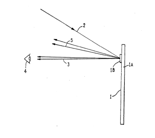
Figure 1 illustrates a first example of a device whileexposed to white light;
Figure 2 illustrates apparatus for reading the machine
readable pattern reconstructed by the device shown in
Figure l;
Figure 3 illustrates an example of a machine readable
pattern; and,
Figures 4 and 5 illustrate apparatus for recording the
first and second diffrac~ive structures respectively.
Figure 1 illustrates a sectional view of a laminated
credit card 1 comprising a security printed, personalised
plastics substrate lA which bears a device lB of the
invention, in the form of a securely affixed label. The
device lB comprises a transparent plastics substrate having
a diffracting inner surface (the diffraction resulting from
an impressed relief pattern), which has becn metallised and
W092/04692 PCT/GB91/01525
.
2 ~ 9 ~'13 ~'
the metallic surface then laminated to the card surface.
The net diffractive embossment comprises two superimposed
diffractive patterns, visual and machine readable
respectively, combined during the originatio~ stage, which
provide a white light viewable display hologram and
infrared responsive machine readable information.
Under white light illumination 2, the device generates
a first reconstructed pattern defining an image which is
perceived to be close to the real plane of the device (as
distinct from appearing to be distantly above or below the
surface o~ the device). This reconstructed image is
~ormed by dif~racted beams 3 which give the perception to
the viewer 4, of typically a three dimensional object.
The image perceived at 4 is kept sharp but is
restricted in perceived position and depth within a
relatively shallow distance above and below the surface of
the device, typically less than 50 mm.
The machine readable feature incorporated in the
composite hologram is reconstructed by the white light 2
such that the image forms well out of the plane of the card
1, typically between 50mm and 300mm away so that it
exhibits a degree of blur due to chromatic aberration.
The net effect of this is that the machine readable image
which would theoretically be viewable in white light as a
result of reconstruction beams 5 is not readily noticeable.
Figure 2 illustrates the apparatus needed to
reconstruct or form the machine readable pattern arising
from the second diffractive structure A solid state
device 11 such as an infrared emitting diode or a laser
diode which preferably emits narrow band near infrared
radiation, typically around 950 nm is collimated or focused
(not shown) in such a way as to provide a beam 12 which
impinges on the composite device lB mounted on the
substrate lA~ Under illumination at this wavelength, the
second pattern generating structure responds to the
incoming beam to reproduce the machine readable pattern
which is in the form of a set of pixels having on or off
w092/0~692 PCT/GB91/Ot525
~9 ~ 16
status (to be described in more detail below), the beams 13
generated by the second structure being focused at 14 onto
one or more photodetectors (or a CCD array) 15. Each
photodetector corresponds to a pixel of the resultant
machine readable image and generates an electrical signal
representing the intensity of the incoming beam. These
electrical signals are fed to processing electronics 16 of
conventional form which compares the detected pattern with
a reference and indicates whather or not the two patterns
are the same~
The first diffractive structure also responds to the
in~rared beam 12 but by selecting the reference to object
beam angle of the first diffractive structure (display
hologram) and the second diffractive structure (machine
readable hologram) it is possible to arrange that at the
infrared readout wavelength, the diffraction angle of the
first order display hologram is greater than 90 so that
the "reconstructed" beam 17 becomes evanescent and does not
exist. This increases signal to noise ratio for the
machine readable pattern.
As has been mentioned above, the composite hologram
could be created by exposing a light responsive surface on
the substrate through an aberrated optical system. In
that case, the machine readable apparatus will further
comprise a de-aberrating optical system (not shown) through
which the reconstructed beams 14 pass before impinging on
detectors 15~
Figure 3 illustrates a typical pixel pattern forming
a machine readable pattern. This pattern, as shown at
21 can be an array of output spots forming an on/off
pattern, bar code and the like or could optionally be well
separated spots or just one spot for verification. In
this particular example, a rectangular array of spots is
shown with pixels 22 being "off" as indicated by the
hatched lines; pixels 23 being "on"; and some pixels 24
having an intermediate (grey scale) value which could be
W092/04692 PCT/GB91/0l525
17 2 ~9 0ll3 ~
used to provide additional encoding in accordance with the
brightness levels.
To produce the diffractive structure which will
reconstruct such a machine reada~le pattern, the
origination target could be a masXed diffuser or set of
diffusers.
To detect this pattern the p~otodetectors 15 or CCD
array will be arranged in a similar manner to the squares
or pixels shown in Figure 3.
Figures 4 and 5 illustrate a two step, optical bench
manufacturing method used for recording both a standard
display hologram as the first diffractive structure and on
top of that the second machine readable diffractive
structure in a recording medium such as a photoresist.
This involves the first step of exposing a photoresist
coated glass plate to form a standard rainbow holographic
image as known in the art.
This is followed by recording on the ~hotoresist the
machine readable diffraction pattern.
Figure 4 shows an illustrative layout for recording a
display hologram. A beam of appropriate laser light is
split. One part forms a collimated or near collimated
reference beam 30 which plays on a photoresist coating 31
mounted on a glass plate 32~ The other part 33 of the
beam is caused to illuminate the rear of a master `(usually
termed "Hl") rainbow hologram (which is a transmission
hologram recorded in a gelatino silver halide emulsion 34
supported on as glass plate 35, which has been developed).
The diffracted light beam 36 reconstructs a real image in
the plane of the photoresist plate, interfering with the
reference beam.
The display hologram of the first diffractive
structure is formed by recording the interference pattern
formed between the object and reference beams, as known in
the art.
Figure 5 illustrates the layout needed on the optical
bench for the recording of the second diffractive
W092/04692 ~ PCT/GB91/01525
~ 18
structure. This is done by placing the photoresist
coating exposed in the manner of Figure 4 before
development.
The photoresist coating 31 is expose~ to a collimated
reference beam 37 and several object beams 38 and 39, each
of which interferes with the reference b~am to form simple
sinusoidal gratings superimposed on the display hologram.
Each of these gratings corresponds to one element of the
machine readable feature~
Alternatively the coded object beams could be derived
from small point sources or small area sources in which
case the machine readable ~eatures would contain a qreater
range o~ spatial frequencies. The advantage of recording
the machine readable feature as a set of overlaid gratings
is the reduction of fringe competition in the medium
allowing a brighter display image and machine readable
image to be observed. In all cases the relative energies
of the exposures are balanced to obtain the derived result.
The machine readable structure will typically be
recorded at a small angle to the reference beam 37 (ie
preferably but not necessarily the same reference beam
angle as the visual image and with a small angle between
the object beam and referènce beam in order to make the
feature more difficult to view). The anqle between the
machine readable object beam and reference beam should be
smaller than that between the visual hologram object beams
(conventionally the angle subtended by the Benton or
rainbow slits of the ~ologram) and the reference beams in
order to aid concealment. It should be noted that the
reference beam for the machine readable pattern could have
a different divergence/convergence to that used for the
visual hologram.
The first illumination source may be a white light
source or less preferably a coloured light source. The
white light incident on the device is preferably angularly
incident from a discrete source rather than diffusely
incident.
W092/04692 PCT/G891/01525
2 Q 9 ~ s~
19
The second illumination source may be a narrow band
source, say, of 50mm bandwidth or less and must emit at a
wavelength substantially different from that of the first
source. The second source is preferably a narrow band
S near infrared source such as is emitted from an infrared
emitting diode and is preferably incident on the device as
a single narrow width beam.