Note: Descriptions are shown in the official language in which they were submitted.
W092/02076 PCT/CA91/0026D
203~7~ll
POWER SUPPLY FOR SINGLE PHASE BOOST
Field Of Invention
This invention relates to a SWII'CH MODE POWER SUPPLY
TO PRODUCE A REGULATED AC OR DC OUTPUT FROM AN UNREGULATED
5 DC SOURCE.
sackaround Of_Invention
The engine on a vehicle drives an alternator which
generates an unregulated alternatin~ current (AC) which is
rectified to provide a direct current (DC) power source
10 which is used to recharge the battery which is necessar~ to
start the engine and also maintain the electrical systems
which are used on the vehicle.
The alternating current (AC) of the alternator is
passed through a rectifying circuit, normally a bridge
15 rectifier or a half bridge rectifier in order to produce a
DC power source. With constant excitation the alternator
will produce an AC voltage which is proportional to the
speed of the engine. Further, the AC vo~tage will have a
frequency which is directly dependent upon the speed of the
20 engine. In this unregulated form, i.e. without a fixed
frequency, the output of the alternator is unsuitable for
powering AC devices which are normally available for
household use. In particular, such AC source is unsuitable
to power sensitive instruments or devices such as computers
25 or other electronic devices which require a constant
frequency and voltage, normally 60 Hz at 120 Volts AC.
In remote areas or construction sites, the only
available source of power may be a vehicle. Therefore, it
.'SUBSTITUTE SHEET
.. , , - , . ......................... . . .
` , . ., . . ~ .
, . .. -; . . . ~ . ~ .
W092/02076 PCT/CA91/00260
2 ~ a~ 2 ~ - 2 -
would be desirable if the vehicle engine could be used as a
source to operate power hand tools or operate electronic
equipment.
To produce a regulated AC supply from existing
5 technology, devices generally comprise a first stage which
produces a DC voltage in excess of a desired AC peak
voltage. TAe second stage of the standard technology
involves an inverter circuit fed by the DC voltage source.
Since the output requires a smooth sine wave generation, a
10 high frequency converter mode is required. Transistor
switching has been found to be the only acceptable method
for such high frequency switching. However, it has been
~ound that since the desired output AC voltage is 120 volts
AC, the stress on such switching components for such
15 compon~nts to operate is at the upper limit. The result is
that the switching transistor~ produce a considerable
voltage drop at higher voltages and accordingly become very
inefficient.
Further, the existing technology generally utilises
20 transistor switching devices in series with the load
increasing the voltage drop and thereby resulting in poor
control capability of the load.
Summary O~ Invention
The disadvantages of the prior art may be overcome by
25 providing a direct converter combining a high frequency
switch mode to boost the voltage to the desired voltage
level and at the same time modulating the converter to
produce a direct sinusoidal output at the load.
: .: . . . . : . .
: ~. . . . ~ -
W~92/02076 PCT/CA91/00260
2a3~72~
It is an object of the invention to provide a 115
Volt nominal regulated sinusoidal AC power supply from an
unregulated ~C source which has a size and weight suitable
for installation on small vehicles.
It is a further object of the invention to provide an
AC power supply which can be used ~or a wide range of loads
for a power tool application where the power factor is
between 0.4 lagging and 1.
It is further object of this invention to have an AC
lO power supply which is switchable between an AC supply and a
~C supply to be able to utilize the high voltage DC power.
According to one aspect of the invention there is
providPd a DC to AC power converter, comprising a converter
circuit connectable to a DC source, and including a
15 plurallty oS switch mean~ which converts the DC source to AC
by alternately switching between the switch means. A
transSormer means is provided Sor transforming the output of
the converter circuit. A filter means is provided which is
connectable to an AC output and having a plurality of
20 damping modes for extracting a fundamental frequency from
the output of the transformer means. A sine wave oscillator
is provided Sor generating a sine wave at the ~undamental
frequency. Feedback means is provided for switching the
Silter means between damping modes after comparing the
25 output of the filter means with the sine wave to maintain
the AC output at the fundamental frequency.
Description Of Drawings
.. . , -, ~: .
.
:- ~ , : , . . ~ , .
: :: , . . ; . : . ~. . . ..
W092/02076PCT/CA91/00260
2 ~
In drawings which illustrate embodiments of the
invention,
Figure 1 is a circuit diagram of the low voltage
stage of the preferred embodiment,
5Figure 2 is a circuit diagram o~ a high voltage
stage of the preferred e~odiment,
Figure 3 is a circuit diagram of a second embodiment
of a high voltage stage,
Figure 4 is a circuit diagram of a third embodiment
10of the high voltage stage,
Figure 5 are graphs illustrating the wave forms at
the load of the preferred embodiment, and
Figure 6 is a block diagram o~ the reactive power
compensating the feed~ack circuit.
15 Note that in the drawings the (.) convention is used to
illustrate a current entering the dotted end of a winding
and sets up a positive flux in the winding.
Detailed ~escription of the Preferred Embodiment
The pre~erred embodiment generally comprises a first
20 stage for con~erting the unregulated low voltage DC source
directly to a high voltage pulse width modu}ated (PWM)
representation o~ a sinusoidal alternating current, without
going through the switching o~ high frequency, high voltage
DC rail. The second stage ~ilters the PWM sinusoidal
25 representation, comp~ensates t~a load impedance in order to
produce a constant Rinusoidal current and voltaqe output at
the load.
~..... ,, . .. , , . . ... . .. . ~ ,. ~ .
" .: . . . , ,. . . ., . . .,... , ~ , . : .
. :: . . ~- : : . ~ . ' :
:: ~.. . - .. : .
, , . - . .
W092/02076 2 a 9 ~ 7 ~ '~ PCT/CA91/00260
- 5 -
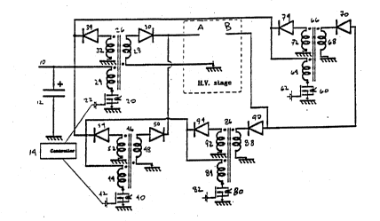
With reference to Figure 1, a circuit diagram is
illustrated representing the first ~tage of this dual ended
power supply.
An unregulated DC voltage supply ].0 is applied across
5 storage capacitor 12 with the polarity indicated. DC source
may be obtained by rectifying with an unregulated
commercial bridge circuit, for example, the output of an
automotive alternator (not illustrated).
Capacltor 12 is connected between voltage supply 10
10 and ground. The positive side of capaci~or 12 is connected
to one end of primary winding 24 of transPormer 26. The
other end o~ winding 24 is connected to a switch means
MOSFET 20 which in turn is connected to ground. MOSFET 20 is
switched between its on and off state by dri~er 22 which is
15 responsive to signals generated by controller 14.
The positive side o~ capacitor 12 is also connected
to diode 34 which in turn is connected to one side of reset
winding 32 of trancformer 26. The opposite end of reset
winding 32 is connected to ground.
Transformer 26 has two primary windings, namely
primary winding 24 and reset winding 32. On the secondary
side of the transformer i5 secondary winding 28 which has
on~ end connected to ground and the other end flowing to
point A through diode 30.
The primary side o~ transformer 26 must be wired and
wound in such a manner that when MOSFET 20 is switched to
its on state allowing current to flow from DC source 10 to
ground by primary winding 24, a positive voltage with
' '.
~,. . . . . . .
:. - . . . . . , ~
.: . .. , : .. , ~.
: . - . .:
W092/02076 PCT/CA9l/00260
2~7~
- 6 -
respect to ground will be induced in secondary winding 28.
When MOSFET 20 is ordered to its off state a path will be
provided by reset winding 32 and diode 34 to allow the flux
of the transformer 26 to be reduced t:o zero. Diode 34
5 permits current to flow only in ~he direction illustrated to
permit the flux to be raset. Similarly for the secondary of
transformer 26, diode 30 has a polarity to restrict the flow
of current in the direction illustrated.
Transformer 46 is wired in an identical fashion as
10 with transformer 26. The DC source 10 has a path to primary
winding 44 then through MOSFET 40 and then to ground. MOSFET
40 is driven by driver 42 which switches MOSFET 40 between
its on and off states. Transformer 46 has a flux resetting
path via reset winding 52 connected to diode 54 which in
lS tUrn is connected to DC source 10. on the secondary side of
transformer 46, secondary winding 48 is connected between
ground and point A having diode 50 to restrict the flow of
current in the desired direction ac shown.
:~ .
Transformers 26 and 46 are referred to as the
20 positive cycle portion of the circuit and operate only
during t~e gensration of a positive voltage.
Transformers 66 and 86 operate only during the
generation o~ a negative voltage. Transformers 66 and 86 are
identical to transformers 26 and 46.
Transformer 66 has a primary winding 64 connected to
a MOSFET 60 connected to ground! Driver 62 which is
responsive to signals from controller 14 and switches MOSFET
60 between its on and off state.
' ~
.'
.~
:.~ , ,,,, - : .. ., . - ~ .
:.-::: : .
:......................... . . .
.: . : . ~ . . . . .
: :: ~ ~ ::: .: . - : .
W092/~2076 PCT/CAgl/00260
2~72~
-- 7 --
~ ransformPr 66 is also provided with reset winding 72
and diode 74. On the s~condary side of trans~ormer 66 is
provided secondary winding 68 and diode 70.
In a similar fashion transformer 86 has primary
5 winding 84 connected to MOSFET 80 connected to ground.
MOSFET 80 is driven by driver 82 which is responsive to
signals from controller 14 fox switching MOSFET 80 between
its on and off state. Transformer 86 has a reset winding 92
connected between ground and diode 94~ On the secondary side
10 of transformer 86 is secondary winding 88 and diode 90.
Tran~fo~mers 66 and 86 are wired in identical manner
as transformers 26 and 46 with the exception that secondary
of transformers 66 and 86 have a polarity opposite that of
the secondary of transformers 26 and 46. The secondary of
15 trans~ormers 66 and 86 accordingly produce a negative
voltage at point B with respect to ground.
With reference to Figure 2, the high voltage stage
circuit, corresponding to the dual ended low voltage stage,
is illustrated including the secondary windings of
20 transformers 26, 46, 66 and 86 up to point A and B
respectively.
Point A is connected to Silicon Controlled Rectifier
(SCR) 102 and then connected in parallel to one side of load
108 through inductor 110. SCR 112 provides a switchable
25 short circuit pa$h across inductor llO. Capacitor 104 is
connected across load 108. Point A is negatively clamped to
ground via diode 106.
, ' . .
'.
-
:: . : . : . . .:
. :. : , .: . : ::.
W092/02076 PC~/CA91/00260
2~9~72~l
Point B is connected to load 108 and capacitor 104 inthe same manner as the connections between point A, with the
exception that all elements are connected with a reverse
polarity. Point B is connected through sc~ 114 which in turn
5 is connected to inductor 120. Inductor 120 is connected in
parallel to SCR 115 to provide a switchable short circuit
path. A positive clamping path is prov:ided between ground
and point B via diode 116.
In figure 2, capacitor 104 is illustrated as a single
10 capacitor. In the preferred embodiment, capacitor 104 is a
bank of capacitors in parallel having a control means to
switch between banks of capacitors. The switching may be a
triac or relay which is responsive to a signal generated by
the comparator. The operation of the control circuit is
i 15 discussed below. Capac~tor 104 will switch capacitor
elements into or out of the circuit to increase or decrease
the total amount of capacitance.
The output of the first stage is a pulse train or a
succession of short width modulated pulses. Each
,~ 20 transformer 26, 46 provides a positive pulse width modulated
voltage, and each transformer 66, 86 provides a negative
pulse width modulated voltage to the high voltage stage
between points A and B. The pulses are divided into
positive groups and negative groups. Each group is active
25 for only one half of a cycle at the fundamental frequency.
' :.'`.
.. . . . . ..
: . : : : . . -
:: . .. - - : . , ,
: .: , . . - ., - ~,, , . . - . -
.-.: ,: ,: - : , .
: ::: . . . . :
W092/02076 PCT~CA91/00260
2 ~ 9 ~
g
The positive group will alternate pulses between
transformers 26 and 46, allowing each coil to reset its flux
while the other conducts. The negative group will similarly
alternate negative pulses between trans~ormers 66 and ~6.
In a typical positive cycla of the pulse train,
MOSFET 20 is turned on and off by its dx.iver 22 which is in
turn enabled by controller 14. Current f:Lows fro~ DC source
10 to ground via primary winding 24 of transformer 26.
Current through the primary winding 24 induces a secondary
10 voltage in the secondary winding 28 allowing a current to
flow through diode 30 to point A.
When controller }4 orders MOSFET 20 to an off state,
the ferrite transformer core 26 resets its flux via diode
34. A current will flow through reset winding 32 in a
15 direction such as to oppose the flux set up by prlmary
windlng 24. This current flow will cause the flux of
transformer 26 to be reset.
At the same time controller 14 may order ~O~FET 40 to
the on state, through its driver 42. Similarly current flows
20 from DC source 10 to ground via primary winding 44 inducing
a secondary voltage in the secondary winding 48 allowing a
current to flow through diode 50 to point A.
When controller 14 turns MOSFET 40 off, the core ~lux
of transformer 46 is reset by the regenerative current
25 flowing through diode 54 via winding 52 from ground to DC
source 10.
Controller 14 continues to switch MOSFET 20 and 40
alternatively and modulates the time between on and off
W092/02076 PCT/CA91/00260
2~9n72~
-- 10 -- ~
states of each switch in such a way that the flux under the
positive voltage appearing between point A and ground
approximates a Pulse Width Modulation (P~M) sine wave.
Controller 14 will continue to alternately turn on
5 and off MOSFET 20 and 40 for the desirecl period of time to
achieve a half cycle for a fundamental frequency. At the end
of the half cycle, controller 14 will cease to alternately
switch on and off MOSFET 20 and 40. Controller 14 will then
alternately switch MOSFET 60 and 80 by turning on and off
10 the drivers 62 and 82 respectively. This will modulate the
negative half cycle of the fundamental sine wave between
point B and ground, using the same PWM technique. The
process is then repeated between positive and negatlve
groups.
15Controller 14 utilizes a switching re,gulator which i9
com~ercially a~vailable as SG 2526 and configured to send out
" 20 micro second pulses alternately between two channels.
The regulator compares an attenuated and rectified version
of the output voltage to a rectified version of a stable 60
20 Hz sinusoidal reference. Whenever the instantaneous
magnitude of the feedback voltage is less than the
instantaneou's magnitude of the reference voltage, the
regulator will maintain the pu~se in order to deliver more
energy to the load, i.e, to increase the output voltage.
25 When the instantaneous magnitude o~ the feedback voltage
exceeds tAe instantaneous magnitude of the reference
voltage, the regulator cuts short the 20 microsecond pulse,
stopping the deliver of energy to the load, thereby causing
- . . :
:: .
:~ .: ..
: ' '.,. , : . - ~
W092/02076 PCT/CA9l/00260
2~7~ ~
-- 11 --
the output voltage to drop. The controller 14 adjusts the
output 833 times in a cycle to generate a positive pulse
train and a negative pulse train which simulates a
sinusoidal output.
In the same fashion as the positive cycle the flux of
transformers 66 and 86 are reset when the respective MOSFET
60 and 80 are in the off state via diode 74 and 94 connected
between reset winding 72 and 92 respectively and DC source
10 .
The output of the first stage at point A and B with
respect to ground is an alternating voltage alternating
between a positive vo}tage pulse train and a negative
voltage pulse train at a fundamental 60 Hz ~requency whi~h
is desired at the output load.
In operation, the circuit connected from point A to
ground operates during the positive h~lf cycle. During the
negative half cy~le, the circuit connected between point B
and ground operates.
With reference to figure 2 the details o~ the high
20 voltage stage are now analyzed. Durin~ the positiva cycle,
SCR 102 is continuously triggered at a high frequency and
acts as a closed relay. At the same time SCR 112 is not
triggered and acts as an open circuit. !'
Current flows from point A through SC~ 102 then
25 through inductor 110 to charge capacitor 104 which energizes
load 10~.
When the primary current of transformers 26 and 46
are not being pulsed, that is at the end of the positive
,, .. ~...... , , . ... . . : .
.
, :: ' : '. ~ . : ` : , ` ;
.. ~ . .. ~ ~ . . . .
W092/02076 PCT/CA91/00260
1 7 2 '~ ~:
- 12 -
half cycle of the desired 60 Hz output voltage, or between
pulses in the posi~ive pulse train, the inductor 110 current
flowing through SCR 102 and load 108 will freewheel via
diode 106 since ScR 102 is still conducting. Inductor 110
5 serves as a filtering device for the high frequency voltage
pulses charging up the capacitor 104.
SCR 112 is fired at the end of the positive cycle
shorting inductor 110 and causins its stored flux to
freewheel. SCR 102 will then see a negative voltage coming
10 from capacitor 104 and thereby forcing it to the off state.
Since the load current no longer has a closed path
from source to ground, the load current will have to
freewheel through capacitor 104 causing its voltage to drop.
When the sinùsoidal reference voltages begins its
15 negativie half cycle, the negative group is started up. SC~
114 is then fired continuously while the primary of
transformers 66 and 86 are alternately switched to induce a
negative voltage in the secondary windings 68 and 88. Diode
116 serves as a freewheel~ng path to the negative load
20 current and current in inductor 120.
SCR llS is fired at the end of the negative voltage
hal~ cycle provi~ing a short circuit path for the stored
flux in coil 120, causing a rever3e voltage across SC~ 114
to appear and causing it to turn off. - ;
With reference to Figure 2 and Figures 5 the
operation of a circuit will now be described, showing how a
sine wave output is created when various loads are present. ~ -~
. . - . - . .
:., . , . . . . . .
~ : . , .: , :
:, ... . . . . . .
, . : -
:
W092/02076 PCT/CA91/00260
2~ 7~
- 13 -
When the output voltage of capacitor 104 ~ecomes
zero, coming from a positive value, the inductive load
current will still have a large magnitude. Figure 5a
illustrates the wave forms at that instant.
At the instant Sc~ 112 is fired, the inductor current
is diverted from feeding SCR 102, and hence causing SCR 102
to turn off. At this time, the energy remaining in inductor
110 rapidly dissipates in the freewheeling path of SCR 112.
The load current will then freewh~el into capacitor 104.
There are three possible cases of response depending
upon the relative capacitance values of capacitor 104 and
the impedance of load 108.
An exponential response will exist i~ the load
inductance and the reslstance constitute an overdamped
15 circuit with capacitor 104. An exponential response has a
810pe lower than the desired sinusoidal output as shown in
figure 5b.
If the inductance and resistance of the load resonate
with capacitor 104, an underdamped response either of
20 Figures 5c or 5d exists. On Figure 5c, the capacitor voltage
is entirely contained within the desired sinusoidal voltage.
In Figure 5d, the capacitor voltage has a much higher slope
than the desired sinusoidal voltage.
Normally capacitor 104 has a relative~y small
25 capacitance producing the more common response as
illustrated in Figure 5d.
If the response of Figure sd is obtained during the
negative group, point B with respect to gr~und will not turn
.,,, : , .
.
,
W092/02076 PCT/CA91/00260
2l39a72~ ~
- 14 -
on until time T1 since the controller sees a voltage
magnitude higher than the raference`voltage. At instant Tl,
the controller takes over the capacitor voltage causing the
load voltage t~ become again sinusoidal on a negative
5 surging.
Xowever, if there is enough capacitance in capacitor
104 to produce the response of Figure 5c or 5b, the
controller would immediately cause the negative group to
regulate the output to be sinusoidal.
lo The control s~rategy is to switch capacitor elements
in and out in capacitor bank 104. Each element is switched
using natural co~mutated triacs or fast acting wet contact
relays.
Since there are no problems associated with primary
lS stressas for either o~ the responses for Pigures Sb, 5c, or
5d~ a control strategy is as follows:
During th~ second and third quarters of the si~e wave
i.e. the time from the positive peak to the negative peak,
the difference be~ween the desired and actual output
20 waveforms are fed into an integrator 708. If this
integration results in a positive value, an underdamped
oscillation is assu~ed with initial slope in excess o~ the
re~erence sine wave value as illustrated in Figure 5d. The
controller adds in a step of extra capacitance ~or the next
25 cycle. This is repeated until the response of 5c is
obtained, at which point sinusoidal voltage will be observed
and no error will be detected.
: . " . . . .
, . , ~ .- ~ . . : , :
,: . . .. ::: - : ,: .: : ;: , . , i :
. : . - :, : . . , . . : .
.: . . :. ~: , . :
.. , -, :.. . ... - . , .. :
, .. . : . : - ~
W~92/02076 PCT/CA91J00260
2~7~
- 15 -
If the cap~citance value for capacltor 104 is too
high, the response of the positive cyc}e will loo~ liXe
Figure ~e. After instant To, the slope of the discharge of
the capacitor 104 through load 108 becomes larger than the
5 slope of the desired sine wave and the controller will stop
firing the positive cycle, point A to ground.
This results in a dis~ortion of thle second quarter of
the wave and can be readily detected as a negative
integration output. This is interpreted by the controller
10 and at the next cycle one capacitor bank is disabled.
Lowering the capacitance one step at a time per cycle is
performed until again the response of 5c i5 obtai~ed and a
sine wave produced within accepted tolerance.
With reference to Figure 6 the control circuit of the
15 reactive power compensation circuit is now described. A
sine wave generator 702 generates a smooth sine wave at the
fundamental frequency, corresponding to the image of the
desired output voltage across the load. The output of the
sine wave generator 702 triggers a synchronized 60 Hz clock
20 circuit 703 which provides pulse outputs at each 1/4 cycle
of the sine wave. The output of the sine wave generator 702
is also fed into a differential operational amplifier
circuit 705, along with an attenuated version of the output
voltage 701~ The output of this circuit, which represents
25 the signed instantaneous error of the desired wave with the
actual load wave shape, is fed into an integrator 708 via
switch 707. This switch is selectively enabled/disabled by
the circuit of 703. The integrator 708 output represents the
:. .: .:, : . . , :: .: .
- : . , :: -
. - ~
. .
W092/02076 PCT/CA91/~0260
2l3~a~
- 16 -
error on the flux betwean the desired output and the actual
output during the 2/4 and 3/4 (i.e. from the positive peak,
through zero and to the negative peak). This signal is fed
into comparators 710 and 711. Thesls comparators have
5 individual thresholds, one set Por too little capacitance,
the other for too much capacitance value of capacitor 104.
When the input of either comparator exceeds the preset
threshold of error in the flux, the corresponding comparator
output will go high, and cause the main controller to insert
10 or remove a capacitor element in the bank 104.
Alternately, the differential operational amplifier
circuit 705 may be removed and the output voltage 701 fed
directly to switch 707. This scheme will act in the same
manner with fewer components, at the expense of requiring
15 perfect synchronization to start and stop the integrator
precisely at the peaks of the wave, which is a very
difficult operation to resolYe.
In the preferred embodiment the chopping frequency at
which MOSFET 20 and 40 and MOSFET 60 and 80 alternately
20 switch is ~5 ~ilohertz to produce an output frequency of 60
Hz. The preferred difference between the chopping frequency
and fundamental frequency is at least 400 ti~es.
Transformers 26, 46, 66 and 86 are ferrite
transformers which allow a reduction in size of the magnetic
25 components, both in weight and in volume as compared with
conventional transformer. The ferrite transformers having a
smaller magnetic component help to increase the power
efficiency of the power supply.
... . . . .
.; :; ::: :
:,.,, . . . . - . : .
: . . . , . : ,
: . . .. .: . : ..
:
W092/02076 2 0 9 9 7 2 ~ PCT/CA91/00260
- 17 -
ThP use of MOSFET ~0, 40, 60 and 80 at low voltages
enables the power to be expanded by parallelism without any
special constraints. The use of the ferrite transformers
connected in parallel (i.e. with primary windings in
S parallel and secondary winding in series) reduces current
winding sizes while increasing output voltages and
ultimately output power.
It is necessary to provide the special switching
arrangement, SC~ 102 and 112 and SCR 114 and 115 on the high
10 voltage side in order to produce the alternating output
voltage. Since these switching elements are used at
frequencies in the 60 hertz range and are all naturally
commutated, it is possible to use low cost thyri~tors and
diodes.
In the pre~erred embodiment, inductors 110 and 120
are required ~or the circuit. In pure DC recti~ication in
standard technology, this inductor is generally not
required. However in AC, if inductors 110 and 120 are not
present, the capacitance 104 reflected to the primary side
20 will compensate for the trans~ormer reactance and the net
impedance seen by the primary switch is limited to the
resistance of the wires. Hence peak current 20 to 30 times
the admissible rating appear which rapidly destroy MOS~ETS
20, 40, 60 and ~O.
The values of impedances of inductor 110 and
capacitor 104 combination must be calculated in such a way
as to limit the primary switch current to within the ratings
of the MOSFET switches, as well as to provide good filtering
.. ..
... . . . . .
W092/02076 PCT/CA91/00260
28~a7~4
- 18 -
of the high frequency carrier i~ order that 60 Hz
fundamental output results.
Inductors 110 and 120 may be interphase reactors,
tightly coupled or separate inductors. If interphase
5 reactors are used this ensures that turning SCR 114 on,
while some current may still flow via 102, will force the
latter to turn off by forced commutation. This feature is
used to avoid short circuit impedance to be reflected to the
primary MOSFET switches during transitions between half
10 cycle switching.
With reference to Figure 3 an alternate embodiment of
the high voltage stage is disclosed. Inductors 110 and 120
may be ganged together as illustrated in the circuit
diagram. Functionally the circuit is identical to that ~ `
15 disclosed in Figure 2. The disadvantages are that isolated
windings must be used for the inductors on the sa~e core.
~owever, an advantage can be achieved because complimentary
SCR pairs 302 and 314 may be used. ~ ;
With reference to Figure 4, an other alternate
20 embodiment of the high voltage stage is disclosed. In this
embodiment, SCR 112 and 115 are replaced with diodes 412 and
415 respectively. Although this circuit functions in the
manner described above, the energy stored in inductors 410
and 420 is dissipated through the diodes between pulses,
25 instead of being transferred to capacitor 104 or the load
108. As a result, the efficiency of the circuit is reduced.
If AC loads having a magnetic circuit are to be fed
by the power supply of the preferred embodiment, there mu~t
-, :: :- . .,. - .. ~ .
... ",., , : .. . , - : , . : .. : ., . : .. ~i .:
: ~ ~ - .. : - . :
., . .. : .
. ,
.: , . :
W092/02076 PCT/CA91/0026~
2 ~
-- 19 --
be no DC flux component on the load output. It has been
found that although the low frequency compo~ents are well
balanced, some higher frequency components may fluctuate and
cause a DC drift in the output. A flux e~lualizer circuit may
5 be added to the standard power controller.
A flux equalizer may be obtained by using a low pass
filter to extract the DC drift of the out:put voltage. The DC
drift can now be conditioned and used as an offset feedback
which is added to the output of sine wave oscillator 702 to
10 produce a DC bias correcting the sine wave reference.
This method prevents magnetic circuits from
saturating even when random starts cause magnetic circuits
to be energized at any point during the AC cycle, and hence~
normally would cause initial flux imbalance. The controller
15 will correct this DC offset flux imbalance in a few cycles
and the load will not experience harmonic current due to
core i~balance and therefore will become more e~ficient.
The preferred embodiment has a size and mass suitable
for installation on a vehicle such as a pick-up truc~,
20 tractor or van. The output voltage peak could be sampled and
used to signal a mechanical throttle control when the output
demands cause the voltage to fall below an accepted limit
from the 120 volts AC output to automatically throttle up
the engine of the vehicle to which the unit is connected
25 thereby increasing the output of the alternator and
ultimately the output to maintain a constant output voltage.
Conversely, when the output load is turned off, the
integrator could trigger the mechanical throttle control to
:~ ; , -
:: . . , :-
: , .
W 89~/8~ ~ ~ PCT/CA91/00260
, o
throttle down the car engine reducing the output voltage.
Alternatively, if the engine speed is held constant, then
the sampled peak output voltage could be used to control th~
alternator's field current. In response to a sampled peak
5 output voltage, which is too low, the alternator's field
current would be increased. As a result, the alternator
output would be increased, which would ultimately allow for
an increase in the output voltage.
The preferred embodiments may also be provided with
lO a switch and a DC output. The switch would first switch
between the AC output and the DC output and secondly would
switch the controller 14 from an AC mode to a DC mode.
Controller 14 would modulate the switching between MOSFET 20
and 40 and MOSFET 60 and 80 with a constant pulse width,
15 rather than a sinusoidal modulation. Further, the DC output
would be regulated by varying the width o~ the pulses.
While various changes may be made in detail or
construction, it shall be understood that such changes shall
be within the spirit and scope o f the present invention.
:....... ,,, '
., , ': ,
: ", ' ' . - :
... . ~ - . , - .
~ .