Note: Descriptions are shown in the official language in which they were submitted.
2 ~
LOCAL APPLICATION MICROPROCESSOR BASED
NERVE AND MUSCLE STIMULATOR
FIELD OF THE INVEN~ION
This invention is directed to a TENS-type
5 therapeutic device, in general, and to a microprocessor
controlled TENS-type system, in particular.
BACKGROUND OF T~E INVENTION
The use of electrical energy for the control of pain
is well known. Although the specific physiological
10 explanations underlying electrically derived pain control
are not fully understood, the effects are quite real and
provide a non-drug, non-surgical and non-psychiatric method
of pain control which can be applied to a wide variety of
painful conditions. ;~
Transcutaneous electroneural stimulation (TENS) is
a proven and accepted means of providing relief from many
kinds of acute and chronic pain symptoms. It is an
attractive alternative to pharmaceuticals since it has no
addictive properties. In addition, there are no known side
20 effects to properly applied TENS therapy.
Several theories have been developed to explain the
neurophysiological mechanisms through which TENS can affect
pain perception. The earliest accepted explanation is the
gate control theory, first postulated by Melzack and Wall
25 in 1965 (Melzack, R. Wall P. D., 'iPain mechanisms: a new
theory," Science, Vol. 150, pp. 971-979, 1965). This
theory used data from animal experiments to predict that
stimulation of afferent nerves could inhibit transmission
from both noxious and non-noxious inputs. However,
30 subsequent research with commercially available stimulators
has demonstrated that TENS efficacy cannot be explained by
gate control theory alone (Schmidt R. D., "Presynaptic
inhibition in the vertebrate central nervous system,"
~Eg~n~ Physicol., Vol. 63 pp. 20-86, 1971).
2~i3~00~
More recent studies (Eriksson! M. B . E ., Sjolund, B .
H. and Nielzen, S., "Long term results of peripheral
conditioning stimulation as an analgesic measure in chronic
pain, " Pain, Vol. 6, pp. 335-347, 1979) have shown that
5 TENS efficacy can be greatly enhanced for some patients by
supplementing new stimulation techniques when
unsatisfactory results are obtained with conventional
stimulation. One popular technique incorporates experience
from Chinese electroacupuncture. The discovery that the
10 effects of this technique, as well as those from
acupuncture, can be reversed with an opioid antagonist,
e.g. naloxone hydrochloride (Sjolund, B. H. and Eriksson,
M. B. E., "The influence of naloxone on analgesia produced
by peripheral conditioning stimulation, Brain Res., Vol.
15 173, pp. 295-301, 1979, and Mayer, D. J., Price, D. D., and
Rafii, A., "Antagonism of acupuncture analgesia in man by
the narcotic atagonic naloxone", Brain Res., Vol. 121, pp.
368-372, 1977) suggested the possibility of an endogenous
- opiate system responsible for pain control.
Since 1975, several endogenous, morphine-like
peptides have been isolated (Hughes, J. et al,
"Identification of two related pentapeptides from the brain
with potent opiate agonist activity", Nature, Vol. 258, p.
577, 1975~, including endorphins which have been found in
25 numerous locations within the central nervous system
(Matsukura, S. et al, "The regional distribution of
immunoreactive beta-endorphin in the monkey brain", Brain
Res., Vol. 159, p. 228, 1978).
The above results have led some researchers
(Eriksson, M. B. E., Sjolund, B. H., and Nielzen, S., "Long
term results of peripheral conditioning stimulation as an
analg~sic measure in chronic pain", Pain, Vol. 6, pp. 335-
347, 1979) to the conclusion that more than one
neurophysiological mechanism is involved in modulating
35 through transcutaneous stimulation This theory is
2 ~
supported by clinical studies (Mannerheimer, J. S. and
Lampe, G. N., "Clinical transcutaneous electrical nerve
stimulation", F. A. Davis Company, Philadelphia, pp. 345-
348, 1984) that demonstra~e the different characterlstics
5 shown in Table 1 for conventional and acupuncture-like
TENS.
TABLE 1
Characteristics of TENS Modes ;
10 Characteristic Conventional Acupun- SimNltaneous
cture-like bimodal
Intensity low high combined
Rate high low combined
15 Relief Onset rapid slow rapid
Relief Duration short long long
Accommodation likely unlikely slight
a c c o m -
modation
likely
Naloxone no yes reduced
Reversible effects
Effects
__ -
The listed properties for simultaneous bimodal
stimulation (i.e. combined stimulation modes) use different
stimulation mechanisms and suggest that the effects are
additive. The validity of this assumption has been
demonstrated in case studies (Mannheimer, J. S. et al.
30 above), but more comprehensive research is needed.
Researchers have found that relevant electrical
signal characteristics which must be examined in attempting
to treat a painful sensation include the signal waveform,
pulse repetition frequency, pulse duration, pulse amplitude
35 and pulse modulation characteristics.
SUMMARY OF THE INVENTION
The invention is directed to the application of
improved TENS system technology employing miniature ;
':, ' .:
2 ~
4 --
electronic circuit components to provide a device that can
be integrated into a variety of application-specific forms
that will be operated at specific treatment sites on the
human body. A unique TENS pulse technique has been
5 developed which significantly reduces the power and the
peak voltage requirements at the treatment site. This
significantly reduces or eliminates the unpleasant burning
of the skin under the electrodes typically experienced when
using most currently available TENS units.
The invention uses commercially available electronic
components. Low-profile, surface-mount components are used
in all units integrated into hermetically sealed treatment
packages associated with the invention. A rechargeable,
dry electrolytic battery can be installed in the package to
15 obtain at least eight hours of operation from a single
charge. All external control signals, including ON/OFF,
are keypad entered and put into effect by interaction with
a single microprocessor central processing unit (CPU). The
CPU is programmed with application-specific waveform
20 generating routines. Most treatment locations require a
custom program. Inputs from the user are interfaced to the
CPU where preprogra~med instructions are carried out.
As an optional feature to the basic unit,
preprogrammed routines are stored in a memory, for example,
25 an EEPROM, can be altered or replaced as required by
interfacing a personal computer or other dedicated
controller via an on-board serial interface. Eight (8)
tactile membrane switches can be accessed by the user to
cause changes in the operation of the unit. The switches
30 are configured as follows:
Two (2) switches to increase/decrease fixed
intensity;
Two (2) switches~ to increase/decrease fixed
modulation frequency;
One (1) switch to activate/de-activate modulation
2 ~
5 --
frequency dither;
One (1) switch to activate/de-activate intensity
dither; and
Two (2) switches to turn ON/OFF the power to the
5 unit.
~ dditional switches can be added to increase program
features. Each operation of a switch will cause a single
incremental change in the selected parameter. If the
switch remains closed there will be no further changes in
10 the parameters. This is a safety feature of the unit which
prevents the application of a full power signal to the
electrodes in the unlikely event a switch were to remain
activated.
The invention also relates to the use of a unique
15 pulse train generated from signals developed by a CPU. The
high frequency carrier is selected to match the TENS output
circuitry to the electrode/tissue load at the treatment
site. It has been noted that low frequency pulse
modulation of a high frequency carrier signal penetrates
20 the surface of the skin more easily due to capacitive
coupling than the direct application of the low frequency
modulating frequency, per se. As a consequence, a lower
amplitude pulse can produce the equivalent effec~ at the
treatment site. Because the energy from the modulated
25 pulse is not dissipated in the skin, the presence thereof
has virtually no effect on the skin. This reduces or
eliminates irritating and annoying sensations on the skin
while effecting treatment, as desired. The inherent power
efficiency of this technique results in a longer battery
30 life as an added benefit.
In one embodiment, an electronic package containing
all components can be mounted within a sealed unit made of
neoprene, Lycra Spandex, or other flexible material. The
battery which powers the unit can be installed within the
35 sealed unit and charged using an external charger. The
2 ~
TENS unit is not intended to be used when the charger is
connected to the battery. ~he electronic circuitry is,
preferably, constructed on a flexible printed circuit board
(PCB). This PCB can be shaped into a form that complies
5 with the requirement for the site specific treatment
device.
Thus, the device consists of the electronic package,
electrodes and any appurtenances required to attach the
unit to the treatment area. The overall unit is made so
10 khat it can be worn comfortably for an extended period
during normal human activity.
BRIEF DESCRIPTION OF THE DRAWINGS
Figure 1 is a schematic diagram of a preferred
embodiment of the stimulator of this invention.
Figures 2A and 2B are logic flow charts that
describe the functional sequencing of the invention.
Figure 3 is a graphic representation of the
microprocessor generated driver waveforms produced by the
- invention.
Figure 4 illustrates a moclel of the output
circuitry.
Figure 5 shows the electrical models of the
stimulator wave~orm.
Figure 6 is a graphic representation of the
25 electrode/tissue current/voltage relationship.
Figures 7, 8 and 9 are graphic representations of
the output waveforms associated with under-saturated,
critically saturated and over-saturated transformer
operation.
DE AILED DESCRIPTION OF THE INVENTION
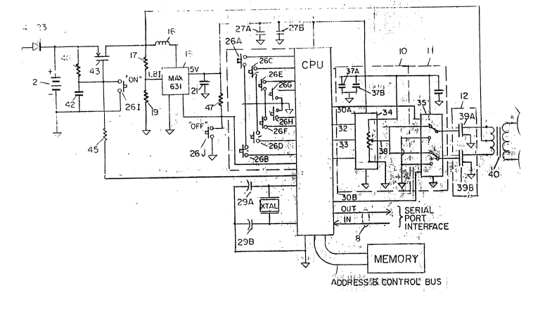
Referring now to Figure 1, there is shown a
partially block, partially schematic diagram of a TENS unit
10 according to a preferred embodiment of the invention.
The data processing functions of the invention are
35 performed by a microcomputer or CPU 1 which is preferably
. " . . ; . " '. . ' ' . ' .' ' ': '
2 ~
a single integrated circuit data processing chip. In a
preferred embodiment, the CPu 1 includes a memory 12. The
memory 12 can take the form of an ele~trically erasable,
programmable, read-only memory such as external EEPROM 20.
5 While not limited thereto, the cPU 1 is preferably a stand
alone, high performance single-chip micro-controller
fabricated in +5 volt advanced CMOS technology so as to
provide low power consumption along with high speed
operation. In the preferred embodiment, CPU 1 is an
10 68HCllE9 device which is available from several
manufacturers and supplies the hardware features,
architectural enhancements and instructions that are
necessary for this invention. External EEPROM 20 is used
by the CPU 1 for storage of the waveform generation
15 programs and interface/"house-keeping" routines required by
CPU 1. In some instances, it is possible to use static
random access memory (SRAM) as the external memory.
All operations of the preferred embodiment of the
invention are carried out through interaction with CPU 1.
20 As noted above, CPU 1 is preferably of the CMOS-type that
is characterized by having an internal control processor
unit (CPU), internal oscillator and timing circuits, 256
bytes of internal RAM, 64 Kbyte bus expansion control, five
programmable I/O parallel ports for address, data bus and
25 I/O pins, two 16-bit timer event counters and a
programmable serial port with a full duplex universal
asynchronous receiver and transmitter (UART) and
synchronous shifter. These components are not delineated
in detail herein. :
The unit 10 is powered by a rechargeable nickel~
cadmium battery 2. Typically, this battery is of a sealed
construction and can be encapsulated within a hermetic
housing (not shown) of the stimulator package. An external
battery charger, which is not part of the invention itself,
35 is used to "re-charge" the battery.
.
2 ~
~.
-- 8
The battery charger is connected to the circuit in
any suitable fashion such as, for example, via jack 24.
The jack 24 is connected to the battery 2 via diode 23.
Diode 23 is connected in series with battery 2 during the
5 charge cycle and is used to prevent damage due to incorrect
charging polarity. The charging current is controlled via
feedback circuitry in the charging unit.
Battery 2, which can be composed of two standard
rechargeable nickel-cadmium cells, provides 2.4 volts to a
10 solid state power switch 14, which produces a regulated 5
volt output. In particular, an RC circuit comprising
resistor 46 and capacitor 42 is connected across the
battery. The anode of battery 2 is connected to the source
electrode of MOS switch 43. The gate electrode of MOS
15 switch 43 is connected to the junction of resistor 46 and
capacitor 42. The gate electrode is also connected to an
output terminal 44 of CPU 1 (described infra). Switch 26I
(a break before make, momentary push button switch) is
- connected across capacitor 42. The drain electrode of MOS
20 switch 43 is connected to the center tap of electrode
isolation transformer 40 and to the common terminal of
inductor 16 and resistor 17. AC-DC converter 18 operates
as a voltage booster and maintains the required 5 volt
signal level at the output thereof by using an internal
25 oscillator and solid state switch to switch inductor 16 in
and out of the circuit. That is, when Vcc falls below the
preset 5 volt value, an error comparator in the converter
18 gates on a 45 kHz oscillator which toggles the internal
N-channel MOSFET ON/OFF.
When MOS gate 43 is ON, the switch closures in
converter 18 during alternate half cycles connect the input
voltage from the battery 2 directly across the inductor 16.
This causes the inductor 16 to alternately charge from the
input battery voltage and discharge at a higher voltage due
35 to the collapse of the residual magnetic fîeld at the
:~
2~
inductor 16. The voltage is discharged into filter
capacitor 21. In order to maintain a constant voltage
across capacitor 21 and load resistor 47, switching pulses
are skipped in proportion to the number of switching cycle~
5 necessary to maintain the level of the output voltage at
the preset level of 5 volts. One example of the converter
18 is a model MAX 631 manufactured by Maxim.
The other terminal of inductor 16 is connected to
the input of DC-DC converter 18. The other terminal of
10 resistor 17 is connected to ground via resistor 19. The
common junction of resistors 17 and 19 is connected to
another input of AC-DC converter 18.
Resistors 17 and 19 form a voltage divider which
sets the threshold for activating low battery indicator
15 signal (LBI) at converter 18. The LBI signal is sent to
the CPU 1. When a low battery signal is received, the
power MOS gate 43 is released by the I/O pin 44 via
software command. This causes the power to be removed from
- the circuit resulting in total shutdown until the batteries
20 are recharged. This operation prevents the possibility of
anomalous operation of the stimulator due to low battery
voltage. The output of the converter 18 is about 5 volts
regulated to stably operate the CPU 1 and the support
circuitry of the stimulator.
Switch 26J (similar to switch 26I) is connected
between an LBO terminal on converter 18 and ground or other
suitable reference voltage. Switch 26J provides an OFF
control for the power switch.
The solid state power switch 14 controls the
30 activation of the system. For example, when the system is
to be turned "ON", switch 26I is momentarily closed,
thereby discharging capacitor 42 to ground. This drives
the gate electrode of MOS switch 43 to ground~ thus turning
the MOS switch ON. When the MOS switch 43 is ON, voltage
35 is applied to the converter 18 which produces +5V and turns
'~,: :
": , . :
" - . . . ,: , .
~9~
-- 10 --
on the cPu 1. Once the CPU l is ON, the "initialize
program" drives the output pin low. With the output pin 44
low, the MOS switch 43 gate electrode is held low via
resistor 45 even after switch 26I has been released.
5 Resistor 46 and capacitor 42 form an RC time constant long
enough to prevent the MOS switch 43 gate electrode from
being pulled to +2.4v via resistor 46 even if the switch
26I is released before the CPU 1 can hold the gate
electrode low. The device is now actively held ON via the
10 CPU 1.
Conversely, the power switch is turned "OFF" by
momentarily closing switch 26J. Switch 26J is connected in
parallel with the open drain output, the LBO of the
converter 18. Resistor 47 pulls the LBO high unless a low
15 battery level or switch 26J pulls the LBO to ground. If
LBO is detected low by the cPu 1, output pin 44 is set high
via software, pulling the gate of the MOS switch 43 to ~5V.
This causes the MOS switch 43 to turn OFF and remove the
battery voltage from the power supply 14. This turns OFF
20 the entire system. Resistor 46 keeps the MOS switch 43
gate electrode at +2.4V and OFF even when the CPU 1 is OFF.
The system can be restarted only by pressing switch 26J.
No power is consumed when the syst:em is OFF because
terminal 44 is a high impedance when the CPU 1 is OFF.
capacitors 27A and 27B are ceramic bypass capacitors
which prevent transients from being conducted to other
parts of the stimulator circuitry. In particular,
capacitor 27A filters high frequency transients from the
input power source to the CPU 1. Capacitor 27B provides
30 the same ~unction for lower frequencie~ that may be present
on the power circuit due to switching transients from the
converter 18 or interaction of the CPU 1 on the power
clrcult .
The CPU 1 is programmed to provide all the necessary
35 functions for operator interface and output signal
: . . - ... : ., ~ :, ., ~
.: . ,, ~ . . ~ , . ; . . .............................. . :
.. . .
2 ~
-- 11 --
interfaces. Additionally, external communications with the
controller are provided via serial communications link 8
that can be accessed for clinical and special application
programming.
Typically, the user controller 20 of the TENS unit
10 includes any suitable devices, such as tactile membrane
switches, that can be located either inside the sealed
package or remotely, as required for application specific
packages.
All user interfaces and input/output (I/O) functions
are effected through the five parallel I/O ports and the
serial port interface. In this em~odiment, controller 20
comprises ten switches, typically in the form of a single
2 x 5 tactile membrane switch keypad. The keypad is used
15 to control the operation of the unit 10 by providing a
means of adjusting parameters through interaction of the
switches with the user. These switches are configured as
follows:
26A - Increase Fixed26B - Decrease Fixed
Intensity Intensity
26C - Increase Fixed26D - Decrease Fixed
Modulation Frequency Modulation
Frequency
26E - Toggle ON/OFF Frequency 26F - Toggle ON/OFF
Dither Intensity
Dither
26G - Toggle ON/OFF Program 1 26H - Toggle ON/OFF
Dither Program 2
Dither
26I - ON Switch 26J - OFF Switch
Frequency reference ~or oscillator 22 and associated
timing circuits is provided by a piezoelectric crystal 25
mounted external to CPU 10. Frequency control crystal 25,
together with capacitors 29A and 29B form the external
35 circuitry for the precision oscillator 22 which provides a
stable frequency source for the operation of the timing and
, ~; - . . : . . .:
. . , . : ~ :
., , ~ :~
2 0 e5~
- 12 -
control functions of the CPU 1. The stable frequency
source assures that frequency dependent functions, such as
pulse width timing (PWT), will be consistent. The
oscillator 22 functions as an integral part of the CPU 1.
5 Capacitors 29a and 29b are selected to assure stable
frequency operation at the desired frequency.
Memory 12 in the form of electrically erasable
programmable random memory (EEPROM) or static random access
memory (SRAM) can be used as external memory for the CPU 1.
10 Internal EEPROM as on the 68HCll is the preferred memory
for the purpose of this invention since program information
recorded in the memory is retained during power off
conditions and can be altered as needed. on the other
hand, external EEPROM allows a larger program to be stored
15 at the expense of more external circuitry.
Bi-phase signals are generated at terminals 3OA and
30B of the CPU 1 and supplied to modulator switch 35. The
up-down signal is supplied to U/D terminal 32 and digitally
controlled potentiometer 34. The level of the U/D signal
20 at the terminal 32 determines whether the potentiometer 34
will be increased or decreased. For example, high voltage
level signals (+Vcc) at terminal 32 allow the potentiometer
34 to be incremented for an increase in resistance value.
Thus, the potentiometer 34 is incremented one step at each
25 transition of the increase signal INC (at terminal 33) from
a high to a low level signal, e.g. from +Vcc to ground.
Conversely, by changing signal U/D from high to low,
e.g. from +Vcc to ground, the potentiometer 34 is
incremented to a lower resistance value by each high to low
30 transition of signal INC at terminal 33. The signal CS is
supplied to a chip select pin of the potentiometer 34 to
enable the potentiometer 34. When the potentiometer 34 is
enabled, it is operative to store the current position
setting in an internal non-volatile memory (NOVRAM), not
35 shown, within the potentiometer 34.
, ,:,, ~ , , : :
: ~ : . . . ~, .
:, . . : ~ . .
- 13 -
Capacitors 37a and 37b form a filter to eliminate
switching transients that may be induced on the ~Vcc power
circuit and that would be sent into the input of the
modulator switch and power drivers.
The voltage at output terminal 38 (vw) is controlled
by the position of the digitally programmed potentiometer
34 and is supplied to the modulator switch 35. Modulator
switch 35 is a conventional CMOS transmission gate and
provides a switching path which alternatively supplies
10 first or second voltage levels to the gate electrodes of a
set of power drivers 39A and 3sB. More particularly, the
switch 35 supplies a low (or ground) level signal to the
power drivers 3sA and 3sB when the switch is electrically
connected to the ground tor other reference) terminals.
15 Alternatively, the switch 35 supplies a different (usually
high) level signal to the power drivers 39A and 39B when
the switch is electrically connected to the VW output 38 of
potentiometer 34.
The position of switch 35 is controlled by the
20 signals Ql and Q2 from output lines 30A and 30B which are
produced by the CPU 1. The voltage signal from switch 35
determines the amplitude and pulse width of the output
signal supplied to the isolation transformer 40 by power
drivers 39A and 39B. That is, battery 2 is connected to
25 supply a positive voltage to the center tap 42 of the
primary winding of transformer 40. The power drivers 39A
and 39B are, typically, enhancement N-channel MOSFETS. The
control voltages, Vgs, and the corresponding drain current,
Id, of the power drivers 3sA and 3sB are controlled by the
30 voltage VW at terminal 3~ which is switched through the
switch 3s.
Amplitude controller 24, which includes digitally
controlled potentiometer 34, is used to control the
amplitude of the signals produced by the CPU 1. In one
35 embodiment, the controller 24 is a Xicor X9C503 which has
. ,: , : .
~, : ::
.:
2 ~
- 14 -
lO0 discrete, stepresistance values and provides a
sufficiently high resolution for this application.
The modulator switch 35 is a CD4053 analog
transmission gate 28. The cPu 1 supplies digital control
5 signals to switch 3S on line DC. Signals from the
amplitude controller 24 are thus switched through the
transmission gate 11 in proper sequence and to the power
drivers 39A and 39B and there used to drive the isolation
transformer 40. The isolation (or matching) transformer 40
10 operates to supply the push-pull waveform generated by the
power drivers 39A and 3sB to the electrodes 41A and 41B.
The transformer 40 also provides a step-up in the level of
the pulse voltage being sent to the electrodes, if desired.
It should be noted that electrodes 4lA and 4lB can vary in
15 size and shape for each application.
Electrodes 41A and 41B are made from conducting
rubber material and can be provided in appropriate si~e and
shape for specific application configurations. These
- electrodes are connected to the output terminals of the
20 secondary winding of transformer 40. Electrodes 41A and
41B are adapted to be applied to the body of the user in
order to effect the proposed treatment.
Thus, in operation, the power switch 14 is turned ON
(as described supra) to connect the battery 2 to the
25 circuit in order to provide the appropriate power. The
switches 26A through 26J are selectively activated to
provide control signals to the CPU 1 (as described infra).
The CPU 1 produce~ output signals which cause potentiometer
34 to increase or decrease incrementally. The
30 potentiometer 34 supplies a selected voltage level to
switch 35. The switch 35 passes signals therethrough as a
function of the Q1 and Q2 signals from CPU 1. The voltage
level passed by switch 35 is applied to the power drivers
39A and 39B to control the signals therethrough and thus
35 through the primary winding of transformer 40. The
, . . , . . .. . .: . ~, .: ,~ . .
:. : , , , ,, . . ~:
.
2 ~ 0
- 15 -
transformer 40 applies (via the secondary winding) the
signals to the elec~rodes 41A and 41B. The electrodes
provide the stimulation to the user to effect the desired
treatment.
The user can control the treatment by selectively
operating the individual switches 26A through 26H of
controller 20. As the switches are operated, the input to
CPU 1 is changed whereupon the outputs therefrom are
changed, as well. As a result, the signals at the
10 electrodes 41A and 41B can be selectively controlled.
Due to the push-pull nature of the transformer
drivers 39A and 39B, the AC voltage and current wavaforms
applied to the tissue are perfectly symmetrical in time and
amplitude. This is important, as waveforms that are net DC
15 but not time symmetric will not result in net zero ion
transfer. This is due to lighter ions carrying most of the
current in the fast portion of the current pulse and
light/heavy ions carrying the current in a slow pulse.
- Figures 2A and 2B are flow charts which illustrate
20 various functions performed by the CPU 1 during the
operation of the present invention. In particular,
referring concurrently to Figures 2A and 2B, there is shown
the operation of the TENS unit 10. When power is initially
applied to the CPU 1 at step 50, certain values are entered
25 automatically so that no waveform will be produced by the
stimulator. ~he next steps involve selection and
initialization of various hardware and software options to
be used to define certain ports as input or output,
initialize output logic states, clear all working internal
30 RAM bytes, define internal processor configurations and
enable interrupts.
Thus, after the initialization of the processor at
step 50, the program initiates the OFF cycle and, at steps
51 and 52, the driver ports Q1 and Q2 are set LOW. Ports
35 Q1 and Q2 corxespond to terminals 30A and 30B on CPU 1 of
,
2 ~
- 16 -
Figure 1. The low level signals at ports Ql and Q2 will
inhibit any driver signals to the CMOS transmission gate
electrodes by switch 35 during the OFF period.
Once the system is fully initialized, the program
5 directs the system to steps 55 and 56, which set
complementary ports Ql and Q2, HIGH and LOW, respectively.
This begins the ON duration (ONDUR) or stimulation
generation subroutine during which a biphasic electrical
stimulation is applied to the tissue via the step-up
10 transformer 40 and electrodes 41A and 41B. The states of
ports Q1 and Q2 are continuously reversed at steps 57 and
58 in a complementary manner for the duration of the
operation until ONDUR = O.
At step 59, DECREMENT ONDUR, the high duration
15 counter is decremented. If the ONDUR counter has not
reached zero, the program will jump back to step 55 and go
through the subroutine comprising steps 55 through 59 until
the ONDUR counter has reached 0.
- When ONDUR = O is detected in step 60, the system
20 jumps to step 54 and resets Q1 and Q2 low. Then it jumps
to the subroutine represented by step 61 and begins to
sequentially read the values in the controller 20 a~
supplied at input terminals 0 through 7 of CPU 1. Thus,
the CPU 1 determines if any of the eight switches 26A
25 through 26B has been pressed.
For example, i~ key O (which corresponds to switch
26A) is closed (or actuated), step 62 of the program will
cause the JUMP Flag to be asserted. AS a result, the
system initiates the subroutine for increasing the
30 intensity of the output signal at the electrodes 4~A and
41B. In this subroutine, step 63 of the subroutine
operates to check for keypress release. It should be noted
that the "check for keypress release" function in each
subroutine automatically puts ports Ql and Q2 in a low
35 state, thereby effectively removing the stimulation signals
. ' ' '`' ' "~' ~.: ' :. ' '' ,,.' . :. ,, ' . , ,
- 17 -
until the key in question is released. Once released, the
ports are reactivated and the program continues. If the
key o is closed at this time, the system will go to step 64
and operate to increment the counter in potentiometer 34.
5 In carrying out this operation, the U/D terminal 32 of CPU
1 in Figure 1 is set high (i. e. the signal U = +Vcc) and
supplied to the digitally controlled potentiometer 34. The
system then checks (at step 65) for the maximum value at
the output of the digital potentiometer 34. If the
10 potentiometer is not at the maximum level as determined by
a software counter, a predetermined number of pulses is
supplied from the CPU 1 counter to the digitally controlled
potentiometer 3~ (at step 66) to increase the resistance
thereof which ef~ects an increase in amplitude of the
15 output signal in accordance with the number of pulses.
Typically, in this embodiment, there are 50 discrete steps
available to the user.
The CPU 1 then returns to the main program and, at
step 67, samples port 1 of CPU 1 to detect whether key 1
(switch 25Bj has been pressed. If key 1 is pressed, the
system initiates the decrease intensity subroutine. In
this subroutine, the system checks for ]cey press release at
step 68 and then, at step 69, operates to decrement the
resistive potentiometer 34. This step sets U/D terminal 32
25 to the low level, i.e. D = ground. This low level signal
is supplied to the digitally controlled potentiometer 34.
At step 70, the system checks for the minimum value at the
output of the potentiometer 34 via the software counter.
If the system is not at the minimum value, step 71 of the
30 subroutine causes a number of pulses to be supplied to
digital potentiometer 34, which will decrement the
potentiometer 34 and decrement the output signal intensity.
The system continues with the main program at step
72 and checks to see if the "key 2 pressed ?" condition
35 exists. If key 2 is pressed, the program will initiate the
:: ~ ~ : - ....
.:
,.
. ,
2 ~
- 18 -
increase fixed modulation frequency subroutine.
At step 73 of the subroutine, the system checks for
keypress release. At step 74, the system operates to
increment an array of values which are loaded into ONDUR to
5 increase the fixed modulation frequency of the output
signal. Typically, this is a ~'look-up table" routine which
loads predetermined values into ONDUR to generate the
designated modulation frequency such that a fixed number of
pulses per second are generated. Typically, this value
10 will range from 2 pulses per second to no pulses per
second.
Once these steps are complete, the subroutine
returns to the main program which, at step 75, determines
if key 3 is pressed. If yes, the system operates the fixed
15 modulation frequency decrease subroutine at steps 75 and
77. ~This is similar to but the inverse of the frequency
increase subroutine of steps 73 and 74. )
The program continues to step 78 to determine if key
4 has been pressed and, at step 79, determines if the key
20 press has been released. If key 4 is pressed, the system
will toggle the frequency dither flag from ON to OFF or OFF
to ON, depending on the current state at step 80. At step
81, the intensity dither flag is reset to prevent both
frequency dither and intensity dither from being active
25 simultaneously.
The system is returned to the main program at step
82 to determine if key 5 is pressed. When key 5 is
pressed, the program will run the intensity dither toggle
subroutine. In this case, the system checks for keypress
30 release (of key 5~ at step 83 and toggles the intensity
dither flag at step 84. At step 85, the maximum dither
intensity is set to the current user set intensity and the
frequency dither flag is reset. This prevents both
intensity and frequency dither from being active
35 simultaneously.
,
. - ~: . : .
:' . : ' ~ : ' : ~ :
, . . . .
Q ~I
.
-- 19 --
The subroutine then returns to the main program and
checks to see if key 6 has been pressed at step 86. When
key 6 is actuated, the program will execute a user program
1 subroutine. This subroutine operates to check for
5 keypress release at step 87, resets both the frequency and
intensity flags at step 88, and loads the variables from
memory to execute user program 1 at step 89.
When kay 7 is actuated (see step 90), the action is
identical to the key 6 actuated subroutine except that the
10 variables from memory are to execute a second program 2.
That is, the keypress release of key 7 is checked at step
91; resets both the frequency and intensity dither flags at
step 92; and loads the program 2 operating variable from
memory in step 93.
Next, the LBO state is tested in step 94. If LBO is
low, the program is terminated by step 95.
After the "key check" steps have been completed (and
LBO is not equal to 1), the system proceeds to the
frequency dither subroutine at tep 96, which is shown in
20 Figure 2B. This subroutine begi:ns by checking the
frequency dither flag set condition at step 97. If the
frequency dither flag is not set, the subroutine goes
immediately to the amplitude modulation subroutine
described infra. If the flag is set, the subroutine checks
25 to see if Dither Direction = DOWN at step 98. If yes, the
subroutine goes to step 99 and checks if ONDUR is at
minimum array value. If yes, the system goes to step 100
to set Dither Direction = UP. If no, the subroutine
decrements the ONDUR array reducing the frequency at step
30 101. . .
However, if Dither Direction = UP at step 98, the
subroutine goes to step 102 to check if ONDUR is at maximum
array value. If yes, the system goes to step 103 to set
Dither Direction = DOWN. If no, the subroutine increments
35 the ONDUR array, increasing the frequency at step 104. ::
`: :
- ~ .
. ..
, ,
- ~..: :.
2 ~
- 20 -
When the system enters the amplitude modulation
subroutine noted above, it also checks to see if the
intensity dither flag is set at step 105. If no, the
subroutine will exit at terminal J (step 150) and return to
5 the primary program as shown in Figure 2A.
If step 105 is yes, the subroutine will check to see
if Dither Direction = DOWN at step 106. If yes, the
subroutine will check if intensity is at the minimum value
at step 107. If yes, the system goes to step 108 to set
10 Dither Direction = UP and then returns to the main program
at step 150 (see also Figure 2A).
On the other hand, if step 107 indicates that the
intensity is not at the minimum, the subroutine decreases
the intensity at step 109 and returns to the main program
15 at step 150.
In similar fashion, if the condition Dither
Direction = UP ~i.e. "NO" indication) is detected at step
106, the subroutine goes to step 110 to check if the
- intensity is at the maximum level set by the user of the
20 device. If yes, the system goes to st:ep 111 to set Dither
Direction = UP. If no, the routine increases the intensity
at step 112 and then returns to the main program at step
150.
As noted, terminal J (or step 150) is the start
25 point for the main program to set port Ql LOW wherein the
sequence begins again. The main program and the several
subroutines continue during operation of the stimulator
until LBO = O or the OFF button 26J is operated .
As noted supra, the switches 26A and 26B are
30 complementary switches as are switches 26C and 26D. Thus,
normally only one of each of these "sets" of switches will
be operated at any time. For example, the output signal
will be "increasing" or "decreasing". Thus, the
appropriate action will be to "increment" or "decrement"
35 the system. In like fashion, the "key pressed" detection
- 21 -
steps are paired in sets. Consequently, it is considered
typical that if "key o pressed" is detected, "key 1
pressed" will not be detected. Thus, alternate subroutines
will be activated and the complementary subroutine will be
5 skipped. For example, if the " increment" subroutine is
activated because key 0 is pressed, it is expected that the
"decrement" subroutine will not be activated because key 1
is not pressed. Thus, the system will jump directly from
step 67 to step 72. The inverse operation is, of course,
10 equally applicable.
Referring now to Figure 3, there is shown a graphic
representation of the output waveforms generated as the
result of the program interaction in the CPU 1 in Figure 1.
The carrier waveforms, A and A' in Figure 3 are bi-phase,
15 complementary pulse signals 118 and 119 generated by a
software subroutine within the CPU 1. Every time this
subroutine is called, four cycles of the carrier frequency
are applied to ports Ql and Q2 in a complementary fashion.
- This carrier frequency (fc) is preset in software to a
20 specific predetermined frequency which is fixed, but load
dependent. That is, the frequency is largely determined by
the size and placement of the electrodes 41A and 41B in
Figure 1. Thus, as the electrode size and/or tissue
varies, the load presented to the transformer secondary
25 also varies. To allow maximum power transfer to the tissue
load, the carrier frequency is adjusted such that Z~ec = ZL
at that fc~ In a preferred embodiment, the carrier
frequency is 1-2 KHz.
The modulation frequency subroutine of waveform 120
30 is user variable (typically from about 2 Hz to 100 Hz) and
is selected by keys 26C and 26D shown in Figure 1 and in
accordance with the operation of steps 72 and 75 shown in
Figure 2A. The ~c routine is "ANDED" with the fm routine in
software. The pulse width of fm is fixed to 4fC with the
35 resulting duty cycle or ON/OFF being variable.
- 22 -
The activation/de-activation of the frequency or
intensity dither is controlled by keys 26E and 26F shown in
Figure 1 and the program operation of steps 78 and 8~ shown
in Figure 2A. When the user presses key 26E or 26F (as
5 detected at the steps 78 or 82), the dither function is
either activated or de-activated. The duty cycle
determines how many of the carrier pulses 121 are driven
onto the electrodes during one f~ period. This is an
important parameter as it determines the average duration
10 of the stimulating pulse and, together with the MOSFET gate
voltage, determines the total energy transferred through
the electrodes to the treatment site. In other words, ~En
the modulation frequency signal 120 is ON, the waveforms A
and A' pass through the gates 38A and 39B as waveforms B
15 and B', respectively. These waveforms are shown as signals
121 and 122, respectively. Conversely, when the modulation
frequency signal 120 is OFF, the waveforms A and A' are
blocked and the signals B and B' remain at a prescribed
- level, e.g. ground. The amplitude of the drive pulses
(i.e. signals 121 and 122) delivered to drivers 39A and
39B, respectively, is variable from Vmin (for example 2.1V)
to Vmax (for example 4.75V) to thereby control the
intensity of the stimulation. The amplitude of the signals
121 and 122 is, of course, controlled by the voltage level
25 of the signal VW supplied by the potentiometer 34 as shown
in Figure 1. Thus, in this embodiment, fifty (50) discrete
steps are provided.
It has been determined that the electrical load
presented to the stimulator pulse is primarily capacitiv~.
30 This capacitive effect is primarily the result of the high
resistance exhibited by the surface of the skin.
Referring now to Figure 4, there is shown a circuit
model of this invention as affected by human skin. In
particular, the MOSFET drivers 39B an~ 39B receive the
35 signals B and B', respectively, from the switch 35 as shown
- 23 -
in Figure 1. The MOSFETS drive the opposite ends of the
primary winding of the transformer 40. The primary winding
is a grounded center tapped 20 winding. The opposite ends
of the secondary winding (which is a l:N ratio relative to
5 the primary winding where N is greater than 1) is connected
to the electrodes 4lA and 4lB, respectively. The
electrodes are placed on the skin of the user. The
intermediate body portion (or "tissue load"~ of the user is
schematically represented as the tissue load 400 between
10 the electrodes. The tissue load 400 includes skin, muscl~,
nerve fibers and the like and is represented by the
electrical analog comprising resistors Rs and Rt as well as
capacitors Cs.
It is known that human skin exhibits a relatively
15 high resistance to the flow of DC electrical current.
Conversely, the subcutaneous tissue layers forming the
muscles and nerve fibers of the body exhibit a relatively
low resistance to the flow of either DC or AC electrical
- current. Thus, in this system, the electrodes 41A and 41B
20 a~pear as plates of a capacitor having a lossy inter-
electrode dielectric 400 which represents the tissue load.
Isolation/step-up transformer 40 (see also Figure 1)
is preferably electrically matched to the electrode/tissue
load at the Fc in order to realize an efficient transfer of
25 electrical impulse energy to the inner tissue and nerve
sites of the body. In the electrical model shown in Figure
4, Rs is the skin bilayer resistance, Cs is the skin
bilayer capacitance and Rt is the extracellular tissue
resistance. For typical body applications, Rt is
30 approximately 100 ohms, but the electrical resistance of
the tissue is dominated by Rs, which is on the order of lOK
ohms. Clearly, the values of Rs and Cs are determined by
the electrode area and interface characteristics with the
skin.
Referring now to Figure 5 there is shown the
- 24 -
primary-referenced equivalent load model for the system
shown in Figure 1. This model represents the operation of
the transformer 40 in this invention. The secondary DC
resistance Rsec, the tissue resistance Rt, and the
5 electrode/tissue capacitance Cs are "reflected" to the
primary side of the transformer by the appropriate use of
the turns ratio N. secause of the relatively low values of
Rs and Rt, as well as the relatively large turns ratio (N)
of the step-up transformer, the respective transformed
10 values will be small compared to the value of primary DC
resistance Rp. Consequently, these transformed values can
be neglected in the analysis. Similarly, the values of
leakage inductance LL and stray capacitance CD are also
small and are also neglected. These assumptions lead to
15 the simplified primary load model wherein the components
within the dashed outline 501 are effectively deleted from
consideration. Thus, it can be easily seen that the model
reduces to a simple RC network compr:ising the primary DC
- resistance Rp and the reflected tissue capacitance N2CJ2.
20 This network is driven by a step voltage G of half period
fc/2, where fc is the carrier frequency. This reactive load
determines the time it takes the primary to reach
saturation. Thus, it determines, in large part, the total
number of primary TURNS together with the range of
25 obtainable carrier frequencies.
It is known that nerve stimulation is effected by
the flow of current through the extracellular tissue
resistance Rt, not by the voltage impressed across the
electrodes 41A and 41B. The maximum current flow in/out of
30 the capacitor defined by the electrodes and, thus, through
Rt, is at the maximum rate of charge of the voltage across
the capacitor. This condition is illustrated in Figure 6
together with timing relation to the microcontroller driver
signals B and B'. It can be seen from the diagram that the
35 carrier frequency fc must be adjusted to allow maximum
2 ~
saturation of the transformer core prior to the
complementary reversal of B and B'. Thus, the maximum core
saturation in transformer 40, coupled with the current
reversal in the primary coil, creates a maximum rate of
5 change in the secondary voltage Vsec and a corresponding
maximum stimulation current Isec through the tissue load
Rt. The selection of the optimum carrier frequency is
highly dependent on the selected matching transformer and
electrode geometry which con~rols C~, as noted supra.
10The secondary TURNS are determined to match the
secondary impedance to the load impedance by an iterative
process between the selection fc , the number of primary
TURNS and the TURNS ratio.
Referring now concurrently to Figures 7, 8 and 9,
15 there are shown waveforms of under-saturated, critically
saturated, and over-saturated operation of the matching
trans~ormer, respectively. In particular, Figure 7
illustrates the maximum secondary load current Ismax
- attainable ~rom optimum core saturation. The optimum
20 saturation is the result of tuning Fc to the OPTIMUM
transformer/electrode/tissue load saturation period
yielding maximum power transfer to the tissue load 400 for
a given transformer configuration. Critical saturation
operation is highly dependent on electrode/tissue
25 capacitance and therefore, requires fc to be tuned to each
electrode geometry as described above. In this case, fc is
selected to be 535 ~z.
Figures 8 and 9 represent the operation of the
identical circuit for which operation is illustrated in
30 Figure 8 but with fc adjusted above (913 Hz) and below (468
Hz) the optimum value, respectively. It can be seen in
Figure 8 that the peak and average secondary current is
well below that obtained in Figure 7. In Figure 9 it is
apparent that the transformer core became saturated with
35 the primary current Ip limited by the DC series resistance
~:
- 26 -
and the same reduction in secondary current amplitude.
This invention develops a uni~ue frequency and
amplitude modulated pulse train. Because of the frequency
modulation of the pulses, the stimulating signal can more
5 easily penetrate the skin thus requiring a lower voltage to
produce the same effèct to the nerve and muscle tissue as
most presently developed conventional stimulators. Also
unique in this invention is the development of application-
specific packages that can be worn and operated thereby
lo permitting treatment during normal human activity.
Conventional stimulators now in use are not easily
adapted to this type of application and this invention
offers a definite advantage gained from this type of
application. A very real advantage is that a person can
15 realize the benefits of TENS treatment while engaged in
normal day to day activity. The invention is developed
from electronic components that are readily available from
several manufacturers. This assures that the invention can
be manufactured and become useful.
Thus, this invention provides a TENS unit employing
a unique output waveform. The unit can be worn by persons
undergoing treatment during normal daily or sports related
activities. The unique output waveform reduces the power
and voltage level requirements of the signal being applied
25 to the treatment area thus significantly reducing or
eliminating the uncomfortable burning sensation normally
associated with most conventional TENS applications. The
unit can be packaged such that all power sources,
electronics, user interface electrodes and application
30 devices (such as wraps or specialty garments) can be
contained in a single composite form. This form is,
typically, application-specific and designed for a
particular treatment locations, e.g., back, neck, leg,
knee, ankle, hip, and the like. All active circuitry and
35 power sourcei can be contained in a single hermetically
~ : ,, . . : :.~ ,., , , ;:: - ,:
- .,~.,, , . ~ , . ,. . , : ,
2 ~
- 27 -
sealed package designed to provide a maximum of safety and
to facilitate ease of operation.
The above description shall not be construed as
limiting the ways in which this invention may be practiced
5 but shall be inclusive of many other variations that do not
depart from the broad interest and intent of the invention.
Thus, there is shown and described a unique design
and concept of a transcutaneous electric nerve stimulation
(TENS) device. The particular configuration shown and
10 described herein relates to electronic stimulators. While
this description is directed to a particular embodiment, it
is understood that those skilled in the art may conceive
modifications and/or variations to the specific embodiments
shown and described herein. Any such modifications or
15 variations which fall within the purview of this
description are intended to be included therein as well.
It is understood that the description herein is intended to
be illustrative only and is not intended to be limitative.
- Rather, the scope of the invention described herein is
20 limited only by the claims appended hereto.
- . ... ~ . . - - . , ~ . - ..
.
.. : .. . , . ~. .. . .
.: ~ ~ : . . ; : . ~: . -
, , : . : : ~
:- : , , , :